Author: mdierolf

  • Beyond the Chatbox: How Anthropic’s ‘Computer Use’ Ignited the Era of Autonomous AI Agents

    Beyond the Chatbox: How Anthropic’s ‘Computer Use’ Ignited the Era of Autonomous AI Agents

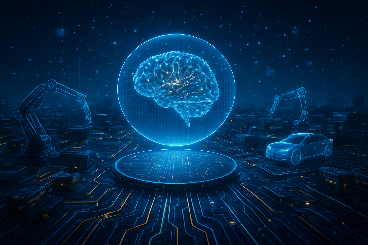
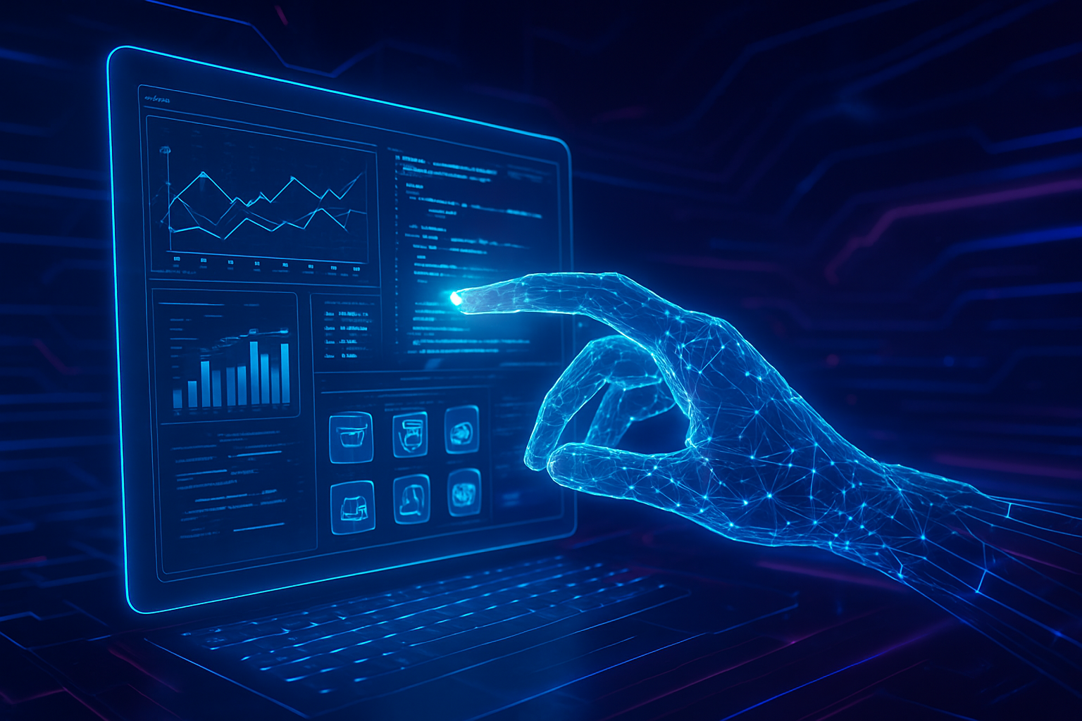
    In a definitive shift for the artificial intelligence industry, Anthropic has moved beyond the era of static text generation and into the realm of autonomous action. With the introduction and subsequent evolution of its "Computer Use" capability for the Claude 3.5 Sonnet model—and its recent integration into the powerhouse Claude 4 series—the company has fundamentally changed how humans interact with software. No longer confined to a chat interface, Claude can now "see" a digital desktop, move a cursor, click buttons, and type text, effectively operating a computer in the same manner as a human professional.

    This development marks the transition from Generative AI to "Agentic AI." By treating the computer screen as a visual environment to be navigated rather than a set of code-based APIs to be integrated, Anthropic has bypassed the traditional "walled gardens" of software. As of January 6, 2026, what began as an experimental public beta has matured into a cornerstone of enterprise automation, enabling multi-step workflows that span across disparate applications like spreadsheets, web browsers, and internal databases without requiring custom integrations for each tool.

    The Mechanics of Digital Agency: How Claude Navigates the Desktop

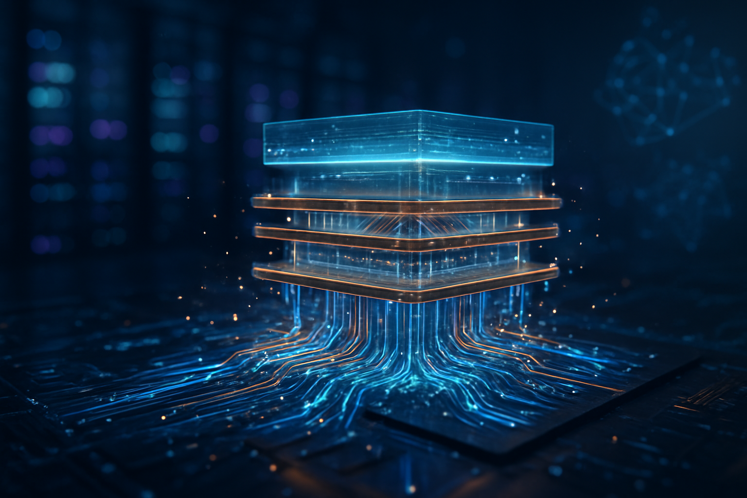
    The technical breakthrough behind "Computer Use" lies in its "General Skill" approach. Unlike previous automation attempts that relied on brittle scripts or specific back-end connectors, Anthropic trained Claude 3.5 Sonnet to interpret the Graphical User Interface (GUI) directly. The model functions through a high-frequency "vision-action loop": it captures a screenshot of the current screen, analyzes the pixel coordinates of UI elements, and generates precise commands for mouse movements and keystrokes. This allows the model to perform complex tasks—such as researching a lead on LinkedIn, cross-referencing their history in a CRM, and drafting a personalized outreach email—entirely through the front-end interface.

    Technical specifications for this capability have advanced rapidly. While the initial October 2024 release utilized the computer_20241022 tool version, the current Claude 4.5 architecture employs sophisticated spatial reasoning that supports high-resolution displays and complex gestures like "drag-and-drop" and "triple-click." To handle the latency and cost of processing constant visual data, Anthropic utilizes an optimized base64 encoding for screenshots, allowing the model to "glance" at the screen every few seconds to verify its progress. Industry experts have noted that this approach is significantly more robust than traditional Robotic Process Automation (RPA), as the AI can "reason" its way through unexpected pop-ups or UI changes that would typically break a standard script.

    The AI research community initially reacted with a mix of awe and caution. On the OSWorld benchmark—a rigorous test of an AI’s ability to perform human-like tasks on a computer—Claude 3.5 Sonnet originally scored 14.9%, a modest but groundbreaking figure compared to the sub-10% scores of its predecessors. However, as of early 2026, the latest iterations have surged past the 60% mark. This leap in reliability has silenced skeptics who argued that visual-based navigation would be too prone to "hallucinations in action," where an agent might click the wrong button and cause irreversible data errors.

    The Battle for the Desktop: Competitive Implications for Tech Giants

    Anthropic’s move has ignited a fierce "Agent War" among Silicon Valley’s elite. While Anthropic has positioned itself as the "Frontier B2B" choice, focusing on developer-centric tools and enterprise sovereignty, it faces stiff competition from OpenAI, Microsoft (NASDAQ: MSFT), and Alphabet (NASDAQ: GOOGL). OpenAI recently scaled its "Operator" agent to all ChatGPT Pro users, focusing on a reasoning-first approach that excels at consumer-facing tasks like travel booking. Meanwhile, Google has leveraged its dominance in the browser market by integrating "Project Jarvis" directly into Chrome, turning the world’s most popular browser into a native agentic environment.

    For Microsoft (NASDAQ: MSFT), the response has been to double down on operating system integration. With "Windows UFO" (UI-Focused Agent), Microsoft aims to make the entire Windows environment "agent-aware," allowing AI to control native legacy applications that lack modern APIs. However, Anthropic’s strategic partnership with Amazon (NASDAQ: AMZN) and its availability on the AWS Bedrock platform have given it a significant advantage in the enterprise sector. Companies are increasingly choosing Anthropic for its "sandbox-first" mentality, which allows developers to run these agents in isolated virtual machines to prevent unauthorized access to sensitive corporate data.

    Early partners have already demonstrated the transformative potential of this tech. Replit, the popular cloud coding platform, uses Claude’s computer use capabilities to allow its "Replit Agent" to autonomously test and debug user interfaces. Canva has integrated the technology to automate complex design workflows, such as batch-editing assets across multiple browser tabs. Even in the service sector, companies like DoorDash (NASDAQ: DASH) and Asana (NYSE: ASAN) have explored using these agents to bridge the gap between their proprietary platforms and the messy, un-integrated world of legacy vendor websites.

    Societal Shifts and the "Agentic" Economy

    The wider significance of "Computer Use" extends far beyond technical novelty; it represents a fundamental shift in the labor economy. As AI agents become capable of handling routine administrative tasks—filling out forms, managing calendars, and reconciling invoices—the definition of "knowledge work" is being rewritten. Analysts from Gartner and Forrester suggest that we are entering an era where the primary skill for office workers will shift from "execution" to "orchestration." Instead of performing a task, employees will supervise a fleet of agents that perform the tasks for them.

    However, this transition is not without significant concerns. The ability for an AI to control a computer raises profound security and safety questions. A model that can click buttons can also potentially click "Send" on a fraudulent wire transfer or "Delete" on a critical database. To mitigate these risks, Anthropic has implemented "Safety-by-Design" layers, including real-time classifiers that block the model from interacting with high-risk domains like social media or government portals. Furthermore, the industry is gravitating toward a "Human-in-the-Loop" (HITL) model, where high-stakes actions require a physical click from a human supervisor before the agent can proceed.

    Comparisons to previous AI milestones are frequent. Many experts view the release of "Computer Use" as the "GPT-3 moment" for robotics and automation. Just as GPT-3 proved that language could be modeled at scale, Claude 3.5 Sonnet proved that the human-computer interface itself could be modeled as a visual environment. This has paved the way for a more unified AI landscape, where the distinction between a "chatbot" and a "software user" is rapidly disappearing.

    The Roadmap to 2029: What Lies Ahead

    Looking toward the next 24 to 36 months, the trajectory of agentic AI suggests a "death of the app" for many use cases. Experts predict that by 2028, a significant portion of user interactions will move away from native application interfaces and toward "intent-based" commands. Instead of opening a complex ERP system, a user might simply tell their agent, "Adjust the Q3 budget based on the new tax law," and the agent will navigate the necessary software to execute the request. This "agentic front-end" could make software complexity invisible to the end-user.

    The next major challenge for Anthropic and its peers will be "long-horizon reliability." While current models can handle tasks lasting a few minutes, the goal is to create agents that can work autonomously for days or weeks—monitoring a project's progress, responding to emails, and making incremental adjustments to a workflow. This will require breakthroughs in "agentic memory," allowing the AI to remember its progress and context across long periods without getting lost in "context window" limitations.

    Furthermore, we can expect a push toward "on-device" agentic AI. As hardware manufacturers develop specialized NPU (Neural Processing Unit) chips, the vision-action loop that currently happens in the cloud may move directly onto laptops and smartphones. This would not only reduce latency but also enhance privacy, as the screenshots of a user's desktop would never need to leave their local device.

    Conclusion: A New Chapter in Human-AI Collaboration

    Anthropic’s "Computer Use" capability has effectively broken the "fourth wall" of artificial intelligence. By giving Claude the ability to interact with the world through the same interfaces humans use, Anthropic has created a tool that is as versatile as the software it controls. The transition from a beta experiment in late 2024 to a core enterprise utility in 2026 marks one of the fastest adoption curves in the history of computing.

    As we look forward, the significance of this development in AI history cannot be overstated. It is the moment AI stopped being a consultant and started being a collaborator. While the long-term impact on the workforce and digital security remains a subject of intense debate, the immediate utility of these agents is undeniable. In the coming weeks and months, the tech industry will be watching closely as Claude 4.5 and its competitors attempt to master increasingly complex environments, moving us closer to a future where the computer is no longer a tool we use, but a partner we direct.


    This content is intended for informational purposes only and represents analysis of current AI developments.

    TokenRing AI delivers enterprise-grade solutions for multi-agent AI workflow orchestration, AI-powered development tools, and seamless remote collaboration platforms.
    For more information, visit https://www.tokenring.ai/.

  • The Silicon Super-Cycle: How the Semiconductor Industry is Racing Past the $1 Trillion Milestone

    The Silicon Super-Cycle: How the Semiconductor Industry is Racing Past the $1 Trillion Milestone

    The global semiconductor industry has reached a historic turning point, transitioning from a cyclical commodity market into the foundational bedrock of a new "Intelligence Economy." As of January 6, 2026, the long-standing industry goal of reaching $1 trillion in annual revenue by 2030 is no longer a distant forecast—it is a fast-approaching reality. Driven by an insatiable demand for generative AI hardware and the rapid electrification of the automotive sector, current run rates suggest the industry may eclipse the trillion-dollar mark years ahead of schedule, with 2026 revenues already projected to hit nearly $976 billion.

    This "Silicon Super-Cycle" represents more than just financial growth; it signifies a structural shift in how the world consumes computing power. While the previous decade was defined by the mobility of smartphones, this new era is characterized by the "Token Economy," where silicon is the primary currency. From massive AI data centers to autonomous vehicles that function as "data centers on wheels," the semiconductor industry is now the most critical link in the global supply chain, carrying implications for national security, economic sovereignty, and the future of human-machine interaction.

    Engineering the Path to $1 Trillion

    Reaching the trillion-dollar milestone has required a fundamental reimagining of transistor architecture. For over a decade, the industry relied on FinFET (Fin Field-Effect Transistor) technology, but as of early 2026, the "yield war" has officially moved to the Angstrom era. Major manufacturers have transitioned to Gate-All-Around (GAA) or "Nanosheet" transistors, which allow for better electrical control and lower power leakage at sub-2nm scales. Intel (NASDAQ: INTC) has successfully entered high-volume production with its 18A (1.8nm) node, while Taiwan Semiconductor Manufacturing Company (NYSE: TSM) is achieving commercial yields of 60-70% on its N2 (2nm) process.

    The technical specifications of these new chips are staggering. By utilizing High-NA (Numerical Aperture) Extreme Ultraviolet (EUV) lithography, companies are now printing features that are smaller than a single strand of DNA. However, the most significant shift is not just in the chips themselves, but in how they are assembled. Advanced packaging technologies, such as TSMC’s CoWoS (Chip-on-Wafer-on-Substrate) and Intel’s EMIB (Embedded Multi-die Interconnect Bridge), have become the industry's new bottleneck. These "chiplet" designs allow multiple specialized processors to be fused into a single package, providing the massive memory bandwidth required for next-generation AI models.

    Industry experts and researchers have noted that this transition marks the end of "traditional" Moore's Law and the beginning of "System-level Moore's Law." Instead of simply shrinking transistors, the focus has shifted to vertical stacking and backside power delivery—a technique that moves power wiring to the bottom of the wafer to free up space for signals on top. This architectural leap is what enables the massive performance gains seen in the latest AI accelerators, which are now capable of trillions of operations per second while maintaining energy efficiency that was previously thought impossible.

    Corporate Titans and the AI Gold Rush

    The race to $1 trillion has reshaped the corporate hierarchy of the technology world. NVIDIA (NASDAQ: NVDA) has emerged as the undisputed king of this era, recently crossing a $5 trillion market valuation. By evolving from a chip designer into a "full-stack datacenter systems" provider, NVIDIA has secured unprecedented pricing power. Its Blackwell and Rubin platforms, which integrate compute, networking, and software, command prices upwards of $40,000 per unit. For major cloud providers and sovereign nations, securing a steady supply of NVIDIA hardware has become a top strategic priority, often dictating the pace of their own AI deployments.

    While NVIDIA designs the brains, TSMC remains the "Sovereign Foundry" of the world, manufacturing over 90% of the world’s most advanced semiconductors. To mitigate geopolitical risks and meet surging demand, TSMC has adopted a "dual-engine" manufacturing model, accelerating production in its new facilities in Arizona alongside its primary hubs in Taiwan. Meanwhile, Intel is executing one of the most significant turnarounds in industrial history. By reclaiming the technical lead with its 18A node and securing the first fleet of High-NA EUV machines, Intel Foundry has positioned itself as the primary Western alternative to TSMC, attracting a growing list of customers seeking supply chain resilience.

    In the memory sector, Samsung (OTC: SSNLF) and SK Hynix have seen their fortunes soar due to the critical role of High-Bandwidth Memory (HBM). Every advanced AI wafer produced requires an accompanying stack of HBM to function. This has turned memory—once a volatile commodity—into a high-margin, specialized component. As the industry moves toward 2030, the competitive advantage is shifting toward companies that can offer "turnkey" solutions, combining logic, memory, and advanced packaging into a single, optimized ecosystem.

    Geopolitics and the "Intelligence Economy"

    The broader significance of the $1 trillion semiconductor goal lies in its intersection with global politics. Semiconductors are no longer just components; they are instruments of national power. The U.S. CHIPS Act and the EU Chips Act have funneled hundreds of billions of dollars into regionalizing the supply chain, leading to the construction of over 70 new mega-fabs globally. This "technological sovereignty" movement aims to reduce reliance on any single geographic region, particularly as tensions in the Taiwan Strait remain a focal point of global economic concern.

    However, this regionalization comes with significant challenges. As of early 2026, the U.S. has implemented a strict annual licensing framework for high-end chip exports, prompting retaliatory measures from China, including "mineral whitelists" for critical materials like gallium and germanium. This fragmentation of the supply chain has ended the era of "cheap silicon," as the costs of building and operating fabs in multiple regions are passed down to consumers. Despite these costs, the consensus among global leaders is that the price of silicon independence is a necessary investment for national security.

    The shift toward an "Intelligence Economy" also raises concerns about a deepening digital divide. As AI chips become the primary driver of economic productivity, nations and companies with the capital to invest in massive compute clusters will likely pull ahead of those without. This has led to the rise of "Sovereign AI" initiatives, where countries like Japan, Saudi Arabia, and France are investing billions to build their own domestic AI infrastructure, ensuring they are not entirely dependent on American or Chinese technology stacks.

    The Road to 2030: Challenges and the Rise of Physical AI

    Looking toward the end of the decade, the industry is already preparing for the next wave of growth: Physical AI. While the current boom is driven by large language models and software-based agents, the 2027-2030 period is expected to be dominated by robotics and humanoid systems. These applications require even more specialized silicon, including low-latency edge processors and sophisticated sensor fusion chips. Experts predict that the "robotics silicon" market could eventually rival the size of the current smartphone chip market, providing the final push needed to exceed the $1.3 trillion revenue mark by 2030.

    However, several hurdles remain. The industry is facing a "ticking time bomb" in the form of a global talent shortage. By 2030, the gap for skilled semiconductor engineers and technicians is expected to exceed one million workers. Furthermore, the environmental impact of massive new fabs and energy-hungry data centers is coming under increased scrutiny. The next few years will see a massive push for "Green Silicon," focusing on new materials like Silicon Carbide (SiC) and Gallium Nitride (GaN) to improve energy efficiency across the power grid and in electric vehicles.

    The roadmap for the next four years includes the transition to 1.4nm (A14) and eventually 1nm (10A) nodes. These milestones will require even more exotic manufacturing techniques, such as "Directed Self-Assembly" (DSA) and advanced 3D-IC architectures. If the industry can successfully navigate these technical hurdles while managing the volatile geopolitical landscape, the semiconductor sector is poised to become the most valuable industry on the planet, surpassing traditional sectors like oil and gas in terms of strategic and economic importance.

    A New Era of Silicon Dominance

    The journey to a $1 trillion semiconductor industry is a testament to human ingenuity and the relentless pace of technological progress. From the development of GAA transistors to the multi-billion dollar investments in global fabs, the industry has successfully reinvented itself to meet the demands of the AI era. The key takeaway for 2026 is that the semiconductor market is no longer just a bellwether for the tech sector; it is the engine of the entire global economy.

    As we look ahead, the significance of this development in AI history cannot be overstated. We are witnessing the physical construction of the infrastructure that will power the next century of human evolution. The long-term impact will be felt in every sector, from healthcare and education to transportation and defense. Silicon has become the most precious resource of the 21st century, and the companies that control its production will hold the keys to the future.

    In the coming weeks and months, investors and policymakers should watch for updates on the 18A and N2 production yields, as well as any further developments in the "mineral wars" between the U.S. and China. Additionally, the progress of the first wave of "Physical AI" chips will provide a crucial indicator of whether the industry can maintain its current trajectory toward the $1 trillion goal and beyond.


    This content is intended for informational purposes only and represents analysis of current AI developments.

    TokenRing AI delivers enterprise-grade solutions for multi-agent AI workflow orchestration, AI-powered development tools, and seamless remote collaboration platforms.
    For more information, visit https://www.tokenring.ai/.

  • The Silicon Sovereignty: How 2026 Became the Year LLMs Moved From the Cloud to Your Desk

    The Silicon Sovereignty: How 2026 Became the Year LLMs Moved From the Cloud to Your Desk

    The era of "AI as a Service" is rapidly giving way to "AI as a Feature," as 2026 marks the definitive shift where high-performance Large Language Models (LLMs) have migrated from massive data centers directly onto consumer hardware. As of January 2026, the "AI PC" is no longer a marketing buzzword but a hardware standard, with over 55% of all new PCs shipped globally featuring dedicated Neural Processing Units (NPUs) capable of handling complex generative tasks without an internet connection. This revolution, spearheaded by breakthroughs from Intel, AMD, and Qualcomm, has fundamentally altered the relationship between users and their data, prioritizing privacy and latency over cloud-dependency.

    The immediate significance of this shift is most visible in the "Copilot+ PC" ecosystem, which has evolved from a niche category in 2024 to the baseline for corporate and creative procurement. With the launch of next-generation silicon at CES 2026, the industry has crossed a critical performance threshold: the ability to run 7B and 14B parameter models locally with "interactive" speeds. This means that for the first time, users can engage in deep reasoning, complex coding assistance, and real-time video manipulation entirely on-device, effectively ending the era of "waiting for the cloud" for everyday AI interactions.

    The 100-TOPS Threshold: A New Era of Local Inference

    The technical landscape of early 2026 is defined by a fierce "TOPS arms race" among the big three silicon providers. Intel (NASDAQ: INTC) has officially taken the wraps off its Panther Lake architecture (Core Ultra Series 3), the first consumer chip built on the cutting-edge Intel 18A process. Panther Lake’s NPU 5.0 delivers a dedicated 50 TOPS (Tera Operations Per Second), but it is the platform’s "total AI throughput" that has stunned the industry. By leveraging the new Xe3 "Celestial" graphics architecture, the platform can achieve a combined 180 TOPS, enabling what Intel calls "Physical AI"—the ability for the PC to interpret complex human gestures and environment context in real-time through the webcam with zero lag.

    Not to be outdone, AMD (NASDAQ: AMD) has introduced the Ryzen AI 400 series, codenamed "Gorgon Point." While its XDNA 2 engine provides a robust 60 NPU TOPS, AMD’s strategic advantage in 2026 lies in its "Strix Halo" (Ryzen AI Max+) chips. These high-end units support up to 128GB of unified LPDDR5x-9600 memory, making them the only laptop platforms currently capable of running massive 70B parameter models—like the latest Llama 4 variants—at interactive speeds of 10-15 tokens per second entirely offline. This capability has effectively turned high-end laptops into portable AI research stations.

    Meanwhile, Qualcomm (NASDAQ: QCOM) has solidified its lead in efficiency with the Snapdragon X2 Elite. Utilizing a refined 3nm process, the X2 Elite features an industry-leading 85 TOPS NPU. The technical breakthrough here is throughput-per-watt; Qualcomm has demonstrated 3B parameter models running at a staggering 220 tokens per second, allowing for near-instantaneous text generation and real-time voice translation that feels indistinguishable from human conversation. This level of local performance differs from previous generations by moving past simple "background blur" effects and into the realm of "Agentic AI," where the chip can autonomously process entire file directories to find and summarize information.

    Market Disruption and the Rise of the ARM-Windows Alliance

    The business implications of this local AI surge are profound, particularly for the competitive balance of the PC market. Qualcomm’s dominance in NPU performance-per-watt has led to a significant shift in market share. As of early 2026, ARM-based Windows laptops now account for nearly 25% of the consumer market, a historic high that has forced x86 giants Intel and AMD to accelerate their roadmap transitions. The "Wintel" monopoly is facing its greatest challenge since the 1990s as Microsoft (NASDAQ: MSFT) continues to optimize Windows 11 (and the rumored modular Windows 12) to run equally well—if not better—on ARM architecture.

    Independent Software Vendors (ISVs) have followed the hardware. Giants like Adobe (NASDAQ: ADBE) and Blackmagic Design have released "NPU-Native" versions of their flagship suites, moving heavy workloads like generative fill and neural video denoising away from the GPU and onto the NPU. This transition benefits the consumer by significantly extending battery life—up to 30 hours in some Snapdragon-based models—while freeing up the GPU for high-end rendering or gaming. For startups, this creates a new "Edge AI" marketplace where developers can sell local-first AI tools that don't require expensive cloud credits, potentially disrupting the SaaS (Software as a Service) business models of the early 2020s.

    Privacy as the Ultimate Luxury Good

    Beyond the technical specifications, the AI PC revolution represents a pivot in the broader AI landscape toward "Sovereign Data." In 2024 and 2025, the primary concern for enterprise and individual users was the privacy of their data when interacting with cloud-based LLMs. In 2026, the hardware has finally caught up to these concerns. By processing data locally, companies can now deploy AI agents that have full access to sensitive internal documents without the risk of that data being used to train third-party models. This has led to a massive surge in enterprise adoption, with 75% of corporate buyers now citing NPU performance as their top priority for fleet refreshes.

    This shift mirrors previous milestones like the transition from mainframe computing to personal computing in the 1980s. Just as the PC democratized computing power, the AI PC is democratizing intelligence. However, this transition is not without its concerns. The rise of local LLMs has complicated the fight against deepfakes and misinformation, as high-quality generative tools are now available offline and are virtually impossible to regulate or "switch off." The industry is currently grappling with how to implement hardware-level watermarking that cannot be bypassed by local model modifications.

    The Road to Windows 12 and Beyond

    Looking toward the latter half of 2026, the industry is buzzing with the expected launch of a modular "Windows 12." Rumors suggest this OS will require a minimum of 16GB of RAM and a 40+ TOPS NPU for its core functions, effectively making AI a requirement for the modern operating system. We are also seeing the emergence of "Multi-Modal Edge AI," where the PC doesn't just process text or images, but simultaneously monitors audio, video, and biometric data to act as a proactive personal assistant.

    Experts predict that by 2027, the concept of a "non-AI PC" will be as obsolete as a PC without an internet connection. The next challenge for engineers will be the "Memory Wall"—the need for even faster and larger memory pools to accommodate the 100B+ parameter models that are currently the exclusive domain of data centers. Technologies like CAMM2 memory modules and on-package HBM (High Bandwidth Memory) are expected to migrate from servers to high-end consumer laptops by the end of the decade.

    Conclusion: The New Standard of Computing

    The AI PC revolution of 2026 has successfully moved artificial intelligence from the realm of "magic" into the realm of "utility." The breakthroughs from Intel, AMD, and Qualcomm have provided the silicon foundation for a world where our devices don't just execute commands, but understand context. The key takeaway from this development is the shift in power: intelligence is no longer a centralized resource controlled by a few cloud titans, but a local capability that resides in the hands of the user.

    As we move through the first quarter of 2026, the industry will be watching for the first "killer app" that truly justifies this local power—something that goes beyond simple chatbots and into the realm of autonomous agents that can manage our digital lives. For now, the "Silicon Sovereignty" has arrived, and the PC is once again the most exciting device in the tech ecosystem.


    This content is intended for informational purposes only and represents analysis of current AI developments.

    TokenRing AI delivers enterprise-grade solutions for multi-agent AI workflow orchestration, AI-powered development tools, and seamless remote collaboration platforms.
    For more information, visit https://www.tokenring.ai/.

  • Shattering the Copper Wall: Silicon Photonics Ushers in the Age of Light-Speed AI Clusters

    Shattering the Copper Wall: Silicon Photonics Ushers in the Age of Light-Speed AI Clusters

    As of January 6, 2026, the global technology landscape has reached a definitive crossroads in the evolution of artificial intelligence infrastructure. For decades, the movement of data within the heart of the world’s most powerful computers relied on the flow of electrons through copper wires. However, the sheer scale of modern AI—typified by the emergence of "million-GPU" clusters and the push toward Artificial General Intelligence (AGI)—has officially pushed copper to its physical breaking point. The industry has entered the "Silicon Photonics Era," a transition where light replaces electricity as the primary medium for data center interconnects.

    This shift is not merely a technical upgrade; it is a fundamental re-architecting of how AI models are built and scaled. With the "Copper Wall" rendering traditional electrical signaling inefficient at speeds beyond 224 Gbps, the world’s leading semiconductor and cloud giants have pivoted to optical fabrics. By integrating lasers and photonic circuits directly into the silicon package, the industry has unlocked a 70% reduction in interconnect power consumption while doubling bandwidth, effectively clearing the path for the next decade of AI growth.

    The Physics of the 'Copper Wall' and the Rise of 1.6T Optics

    The technical crisis that precipitated this shift is known as the "Copper Wall." As per-lane speeds reached 224 Gbps in late 2024 and throughout 2025, the reach of passive copper cables plummeted to less than one meter. At these frequencies, electrical signals degrade so rapidly that they can barely traverse a single server rack without massive power-hungry amplification. By early 2025, data center operators reported that the "I/O Tax"—the energy required just to move data between chips—was consuming nearly 30% of total cluster power.

    To solve this, the industry has turned to Co-Packaged Optics (CPO) and Silicon Photonics. Unlike traditional pluggable transceivers that sit at the edge of a switch, CPO moves the optical engine directly onto the processor substrate. This allows for a "shoreline" of high-speed optical I/O that bypasses the energy losses of long electrical traces. In late 2025, the market saw the mass adoption of 1.6T (Terabit) transceivers, which utilize 200G per-lane technology. By early 2026, initial demonstrations of 3.2T links using 400G per-lane technology have already begun, promising to support the massive throughput required for real-time inference on trillion-parameter models.

    The technical community has also embraced Linear-drive Pluggable Optics (LPO) as a bridge technology. By removing the power-intensive Digital Signal Processor (DSP) from the optical module and relying on the host ASIC to drive the signal, LPO has provided a lower-latency, lower-power intermediate step. However, for the most advanced AI clusters, CPO is now considered the "gold standard," as it reduces energy consumption from approximately 15 picojoules per bit (pJ/bit) to less than 5 pJ/bit.

    The New Power Players: NVDA, AVGO, and the Optical Arms Race

    The transition to light has fundamentally shifted the competitive dynamics among semiconductor giants. Nvidia (NASDAQ: NVDA) has solidified its dominance by integrating silicon photonics into its latest Rubin architecture and Quantum-X networking platforms. By utilizing optical NVLink fabrics, Nvidia’s million-GPU clusters can now operate with nanosecond latency, effectively treating an entire data center as a single, massive GPU.

    Broadcom (NASDAQ: AVGO) has emerged as a primary architect of this new era with its Tomahawk 6-Davisson switch, which boasts a staggering 102.4 Tbps throughput and integrated CPO. Broadcom’s success in proving CPO reliability at scale—particularly within the massive AI infrastructures of Meta and Google—has made it the indispensable partner for optical networking. Meanwhile, TSMC (NYSE: TSM) has become the foundational foundry for this transition through its COUPE (Compact Universal Photonic Engine) technology, which allows for the 3D stacking of photonic and electronic circuits, a feat previously thought to be years away from mass production.

    Other key players are carving out critical niches in the optical ecosystem. Marvell (NASDAQ: MRVL), following its strategic acquisition of optical interconnect startups in late 2025, has positioned its Ara 1.6T Optical DSP as the backbone for third-party AI accelerators. Intel (NASDAQ: INTC) has also made a significant comeback in the data center space with its Optical Compute Interconnect (OCI) chiplets. Intel’s unique ability to integrate lasers directly onto the silicon die has enabled "disaggregated" data centers, where compute and memory can be physically separated by over 100 meters without a loss in performance, a capability that is revolutionizing how hyperscalers design their facilities.

    Sustainability and the Global Interconnect Pivot

    The wider significance of the move from copper to light extends far beyond mere speed. In an era where the energy demands of AI have become a matter of national security and environmental concern, silicon photonics offers a rare "win-win" for both performance and sustainability. The 70% reduction in interconnect power provided by CPO is critical for meeting the carbon-neutral goals of tech giants like Microsoft and Amazon, who are currently retrofitting their global data center fleets to support optical fabrics.

    Furthermore, this transition marks the end of the "Compute-Bound" era and the beginning of the "Interconnect-Bound" era. For years, the bottleneck in AI was the speed of the processor itself. Today, the bottleneck is the "fabric"—the ability to move massive amounts of data between thousands of processors simultaneously. By shattering the Copper Wall, the industry has ensured that AI scaling laws can continue to hold true for the foreseeable future.

    However, this shift is not without its concerns. The complexity of manufacturing CPO-based systems is significantly higher than traditional copper-based ones, leading to potential supply chain vulnerabilities. There are also ongoing debates regarding the "serviceability" of integrated optics; if an optical laser fails inside a $40,000 GPU package, the entire unit may need to be replaced, unlike the "hot-swappable" pluggable modules of the past.

    The Road to Petabit Connectivity and Optical Computing

    Looking ahead to the remainder of 2026 and into 2027, the industry is already eyeing the next frontier: Petabit-per-second connectivity. As 3.2T transceivers move into production, researchers are exploring multi-wavelength "comb lasers" that can transmit hundreds of data streams over a single fiber, potentially increasing bandwidth density by another order of magnitude.

    Beyond just moving data, the ultimate goal is Optical Computing—performing mathematical calculations using light itself rather than transistors. While still in the early experimental stages, the integration of photonics into the processor package is the necessary first step toward this "Holy Grail" of computing. Experts predict that by 2028, we may see the first hybrid "Opto-Electronic" processors that perform specific AI matrix multiplications at the speed of light, with virtually zero heat generation.

    The immediate challenge remains the standardization of CPO interfaces. Groups like the OIF (Optical Internetworking Forum) are working feverishly to ensure that components from different vendors can interoperate, preventing the "walled gardens" that could stifle innovation in the optical ecosystem.

    Conclusion: A Bright Future for AI Infrastructure

    The transition from copper to silicon photonics represents one of the most significant architectural shifts in the history of computing. By overcoming the physical limitations of electricity, the industry has laid the groundwork for AGI-scale infrastructure that is faster, more efficient, and more scalable than anything that came before. The "Copper Era," which defined the first fifty years of the digital age, has finally given way to the "Era of Light."

    As we move further into 2026, the key metrics to watch will be the yield rates of CPO-integrated chips and the speed at which 1.6T networking is deployed across global data centers. For AI companies and tech enthusiasts alike, the message is clear: the future of intelligence is no longer traveling through wires—it is moving at the speed of light.


    This content is intended for informational purposes only and represents analysis of current AI developments.

    TokenRing AI delivers enterprise-grade solutions for multi-agent AI workflow orchestration, AI-powered development tools, and seamless remote collaboration platforms.
    For more information, visit https://www.tokenring.ai/.

  • Silicon Sovereignty: Texas Instruments’ SM1 Fab Leads the Charge in America’s Semiconductor Renaissance

    Silicon Sovereignty: Texas Instruments’ SM1 Fab Leads the Charge in America’s Semiconductor Renaissance

    The landscape of American technology has reached a historic milestone as Texas Instruments (NASDAQ: TXN) officially enters its "Harvest Year," marked by the successful production launch of its landmark SM1 fab in Sherman, Texas. This facility, which began high-volume operations on December 17, 2025, represents the first major wave of domestic semiconductor capacity coming online under the strategic umbrella of the CHIPS and Science Act. As of January 2026, the SM1 fab is actively ramping up to produce tens of millions of analog and embedded processing chips daily, signaling a decisive shift in the global supply chain.

    The activation of SM1 is more than a corporate achievement; it is a centerpiece of the United States' broader effort to secure the foundational silicon required for the AI revolution. While high-profile logic chips often dominate the headlines, the analog and power management components produced at the Sherman site are the indispensable "nervous system" of modern technology. Backed by a final award of $1.6 billion in direct federal funding and up to $8 billion in investment tax credits, Texas Instruments is now positioned to provide the stable, domestic hardware foundation necessary for everything from AI-driven data centers to the next generation of autonomous electric vehicles.

    The SM1 facility is a marvel of modern industrial engineering, specifically optimized for the production of 300mm (12-inch) wafers. By utilizing 300mm technology rather than the older 200mm industry standard, Texas Instruments achieves a 2.3-fold increase in surface area per wafer, which translates to a staggering 40% reduction in chip-level fabrication costs. This efficiency is critical for the "mature" nodes the facility targets, ranging from 28nm to 130nm. While these are not the sub-5nm nodes used for high-end CPUs, they are the gold standard for high-precision analog and power management applications where reliability and voltage tolerance are paramount.

    Technically, the SM1 fab is designed to be the most automated and environmentally sustainable facility in the company’s history. It features advanced cleanroom robotics and real-time AI-driven yield management systems that minimize waste and maximize throughput. This differs significantly from previous generations of manufacturing, which relied on more fragmented, manual oversight. The integration of these technologies allows TI to maintain a "fab-lite" level of flexibility while reaping the benefits of total internal manufacturing control—a strategy the company expects will lead to over 95% internal wafer production by 2030.

    Initial reactions from the industry and the research community have been overwhelmingly positive. Analysts at major firms note that the sheer scale of the Sherman site—which has the footprint to eventually house four massive fabs—provides a level of supply chain predictability that has been missing since the 2021 shortages. Experts highlight that TI's focus on foundational silicon addresses a critical bottleneck: you cannot run a $40,000 AI GPU without the $2 power management integrated circuits (PMICs) that regulate its energy intake. By securing this "bottom-up" capacity, the U.S. is effectively de-risking the entire hardware stack.

    The implications for the broader tech industry are profound, particularly for companies reliant on stable hardware pipelines. Texas Instruments stands as the primary beneficiary, leveraging its domestic footprint to gain a competitive edge over international rivals like STMicroelectronics or Infineon. By producing chips in the U.S., TI offers its customers—ranging from industrial giants to automotive leaders—a hedge against geopolitical instability and shipping disruptions. This strategic positioning is already paying dividends, as TI recently debuted its TDA5 SoC family at CES 2026, targeting Level 3 vehicle autonomy with chips manufactured right in North Texas.

    Major AI players, including NVIDIA (NASDAQ: NVDA) and Advanced Micro Devices (NASDAQ: AMD), also stand to benefit indirectly. The energy demands of AI data centers have skyrocketed, requiring sophisticated power modules and Gallium Nitride (GaN) semiconductors to maintain efficiency. TI’s new capacity is specifically geared toward these high-voltage applications. As domestic capacity grows, these tech giants can source essential peripheral components from a local partner, reducing lead times and ensuring that the massive infrastructure build-out for generative AI continues without the "missing link" component shortages of years past.

    Furthermore, the domestic boom is forcing a strategic pivot among startups and mid-sized tech firms. With guaranteed access to U.S.-made silicon, developers in the robotics and IoT sectors can design products with a "Made in USA" assurance, which is increasingly becoming a requirement for government and defense contracts. This could potentially disrupt the market positioning of offshore foundries that have traditionally dominated the mature-node space. As Texas Instruments ramps up SM1 and prepares its sister facilities, the competitive landscape is shifting from a focus on "cheapest possible" to "most resilient and reliable."

    Looking at the wider significance, the SM1 launch is a tangible validation of the CHIPS and Science Act’s long-term vision. It marks a transition from legislative intent to industrial reality. In the broader AI landscape, this development signifies the "hardware hardening" phase of the AI era. While 2023 and 2024 were defined by software breakthroughs and LLM scaling, 2025 and 2026 are being defined by the physical infrastructure required to sustain those gains. The U.S. is effectively building a "silicon shield" that protects its technological lead from external supply shocks.

    However, this expansion is not without its concerns. The rapid scaling of domestic fabs has led to an intense "war for talent" in the semiconductor sector. Texas Instruments and its peers, such as Intel (NASDAQ: INTC) and Samsung (KRX: 005930), are competing for a limited pool of specialized engineers and technicians. Additionally, the environmental impact of such massive industrial sites remains a point of scrutiny, though TI’s commitment to LEED Gold standards at its newer facilities aims to mitigate these risks. These challenges are the growing pains of a nation attempting to re-industrialize its most complex sector in record time.

    Compared to previous milestones, such as the initial offshoring of chip manufacturing in the 1990s, the current boom represents a complete 180-degree turn in economic philosophy. It is a recognition that economic security and national security are inextricably linked to the semiconductor. The SM1 fab is the first major proof of concept that the U.S. can successfully repatriate high-volume manufacturing without losing the cost-efficiencies that globalized trade once provided.

    The future of the Sherman mega-site is already unfolding. While SM1 is the current focus, the exterior shell of SM2 is already complete, with cleanroom installation and tool positioning slated to begin later in 2026. Texas Instruments has designed the site to be demand-driven, meaning SM3 and SM4 can be brought online rapidly as the market for AI and electric vehicles continues to expand. On the horizon, we can expect to see TI integrate even more advanced packaging technologies and a wider array of Wide Bandgap (WBG) materials like GaN and Silicon Carbide (SiC) into their domestic production lines.

    In the near term, the industry is watching the upcoming launch of LFAB2 in Lehi, Utah, which is scheduled for production in mid-to-late 2026. This facility will work in tandem with the Texas fabs to create a diversified, multi-state manufacturing network. Experts predict that as these facilities reach full capacity, the U.S. will see a stabilization of prices for essential electronic components, potentially leading to a new wave of innovation in consumer electronics and industrial automation that was previously stifled by supply uncertainty.

    The launch of Texas Instruments’ SM1 fab marks the beginning of a new era in American manufacturing. By combining federal support through the CHIPS Act with a disciplined, 300mm-focused technical strategy, TI has created a blueprint for domestic industrial success. The key takeaways are clear: the U.S. is no longer just a designer of chips, but a formidable manufacturer once again. This development provides the essential "foundational silicon" that will power the AI data centers, autonomous vehicles, and smart factories of the next decade.

    As we move through 2026, the significance of this moment will only grow. The "Harvest Year" has begun, and the chips rolling off the line in Sherman are the seeds of a more resilient, technologically sovereign future. For investors, policymakers, and consumers, the progress at the Sherman mega-site and the upcoming LFAB2 launch are the primary metrics to watch. The U.S. semiconductor boom is no longer a plan—it is a reality, and it is happening one 300mm wafer at a time.


    This content is intended for informational purposes only and represents analysis of current AI developments.

    TokenRing AI delivers enterprise-grade solutions for multi-agent AI workflow orchestration, AI-powered development tools, and seamless remote collaboration platforms.
    For more information, visit https://www.tokenring.ai/.

  • The Wide-Bandgap Tipping Point: How GaN and SiC Are Breaking the Energy Wall for AI and EVs

    The Wide-Bandgap Tipping Point: How GaN and SiC Are Breaking the Energy Wall for AI and EVs

    As of January 6, 2026, the semiconductor industry has officially entered the "Wide-Bandgap (WBG) Era." For decades, traditional silicon was the undisputed king of power electronics, but the dual pressures of the global electric vehicle (EV) transition and the insatiable power hunger of generative AI have pushed silicon to its physical limits. In its place, Gallium Nitride (GaN) and Silicon Carbide (SiC) have emerged as the foundational materials for a new generation of high-efficiency, high-density power systems that are effectively "breaking the energy wall."

    The immediate significance of this shift cannot be overstated. With AI data centers now consuming more electricity than entire mid-sized nations and EV owners demanding charging times comparable to a gas station stop, the efficiency gains provided by WBG semiconductors are no longer a luxury—they are a requirement for survival. By allowing power systems to run hotter, faster, and with significantly less energy loss, GaN and SiC are enabling the next phase of the digital and green revolutions, fundamentally altering the economics of energy consumption across the globe.

    Technically, the transition to WBG materials represents a leap in physics. Unlike traditional silicon, which has a narrow "bandgap" (the energy required to move electrons into a conductive state), GaN and SiC possess much wider bandgaps—3.2 electron volts (eV) for SiC and 3.4 eV for GaN, compared to silicon’s 1.1 eV. This allows these materials to withstand much higher voltages and temperatures. In 2026, the industry has seen a massive move toward "Vertical GaN" (vGaN), a breakthrough that allows GaN to handle the 1200V+ requirements of heavy machinery and long-haul trucking, a domain previously reserved for SiC.

    The most significant manufacturing milestone of the past year was the shipment of the first 300mm (12-inch) GaN-on-Silicon wafers by Infineon Technologies AG (OTC: IFNNY). This transition from 200mm to 300mm wafers has nearly tripled the chip yield per wafer, bringing GaN closer to cost parity with legacy silicon than ever before. Meanwhile, SiC technology has matured through the adoption of "trench" architectures, which increase current density and reduce resistance, allowing for even smaller and more efficient traction inverters in EVs.

    These advancements differ from previous approaches by focusing on "system-level" efficiency rather than just component performance. In the AI sector, this has manifested as "Power-on-Package," where GaN power converters are integrated directly onto the processor substrate. This eliminates the "last inch" of power delivery losses that previously plagued high-performance computing. Initial reactions from the research community have been overwhelmingly positive, with experts noting that these materials have effectively extended the life of Moore’s Law by solving the thermal throttling issues that threatened to stall AI hardware progress.

    The competitive landscape for power semiconductors has been radically reshaped. STMicroelectronics (NYSE: STM) has solidified its leadership in the EV space through its fully integrated SiC production facility in Italy, securing long-term supply agreements with major European and American automakers. onsemi (NASDAQ: ON) has similarly positioned itself as a critical partner for the industrial and energy sectors with its EliteSiC M3e platform, which has set new benchmarks for reliability in harsh environments.

    In the AI infrastructure market, Navitas Semiconductor (NASDAQ: NVTS) has emerged as a powerhouse, partnering with NVIDIA (NASDAQ: NVDA) to provide the 12kW power supply units (PSUs) required for the latest "Vera Rubin" AI architectures. These PSUs achieve 98% efficiency, meeting the rigorous 80 PLUS Titanium standard and allowing data center operators to pack more compute power into existing rack footprints. This has created a strategic advantage for companies like Vertiv Holdings Co (NYSE: VRT), which integrates these WBG-based power modules into their liquid-cooled data center solutions.

    The disruption to existing products is profound. Legacy silicon-based Insulated-Gate Bipolar Transistors (IGBTs) are being rapidly phased out of the high-end EV market. Even Tesla (NASDAQ: TSLA), which famously announced a plan to reduce SiC usage in 2023, has pivoted toward a "hybrid" approach in its mass-market platforms—using high-efficiency SiC for performance-critical components while optimizing die area to manage costs. This shift has forced traditional silicon suppliers to either pivot to WBG or face obsolescence in the high-growth power sectors.

    The wider significance of the WBG revolution lies in its impact on global sustainability and the "Energy Wall." As AI models grow in complexity, the energy required to train and run them has become a primary bottleneck. WBG semiconductors act as a pressure valve, reducing the cooling requirements and energy waste in data centers by up to 40%. This is not just a technical win; it is a geopolitical necessity as governments around the world implement stricter energy consumption mandates for digital infrastructure.

    In the transportation sector, the move to 800V architectures powered by SiC has effectively solved "range anxiety" for many consumers. By enabling 15-minute ultra-fast charging and extending vehicle range by 7-10% through efficiency alone, WBG materials have done more to accelerate EV adoption than almost any battery chemistry breakthrough in the last five years. This transition is comparable to the shift from vacuum tubes to transistors in the mid-20th century, marking a fundamental change in how humanity manages and converts electrical energy.

    However, the rapid transition has raised concerns regarding the supply chain. The "SiC War" of 2025, which saw a surge in demand outstrip supply, led to the dramatic restructuring of Wolfspeed (NYSE: WOLF). After successfully emerging from a mid-2025 financial reorganization, Wolfspeed is now a leaner, 200mm-focused player, highlighting the immense capital intensity and risk involved in scaling these advanced materials. There are also environmental concerns regarding the energy-intensive process of growing SiC crystals, though these are largely offset by the energy saved during the chips' lifetime.

    Looking ahead, the next frontier for WBG semiconductors is the integration of diamond-based materials. While still in the early experimental phases in 2026, "Ultra-Wide-Bandgap" (UWBG) materials like diamond and Gallium Oxide ($Ga_2O_3$) promise thermal conductivity and voltage handling that dwarf even GaN and SiC. In the near term, we expect to see GaN move into the main traction inverters of entry-level EVs, further driving down costs and making high-efficiency electric mobility accessible to the masses.

    Experts predict that by 2028, we will see the first "All-GaN" data centers, where every stage of power conversion—from the grid to the chip—is handled by WBG materials. This would represent a near-total decoupling of compute growth from energy growth. Another area to watch is the integration of WBG into renewable energy grids; SiC-based string inverters are expected to become the standard for utility-scale solar and wind farms, drastically reducing the cost of transmitting green energy over long distances.

    The rise of Gallium Nitride and Silicon Carbide marks a pivotal moment in the history of technology. By overcoming the thermal and electrical limitations of silicon, these materials have provided the "missing link" for the AI and EV revolutions. The key takeaways from the start of 2026 are clear: efficiency is the new currency of the tech industry, and the ability to manage power at scale is the ultimate competitive advantage.

    As we look toward the rest of the decade, the significance of this development will only grow. The "Wide-Bandgap Tipping Point" has passed, and the industry is now in a race to scale. In the coming weeks and months, watch for more announcements regarding 300mm GaN production capacity and the first commercial deployments of Vertical GaN in heavy industry. The era of silicon dominance in power is over; the era of WBG has truly begun.


    This content is intended for informational purposes only and represents analysis of current AI developments.

    TokenRing AI delivers enterprise-grade solutions for multi-agent AI workflow orchestration, AI-powered development tools, and seamless remote collaboration platforms.
    For more information, visit https://www.tokenring.ai/.

  • The HBM3E and HBM4 Memory War: How SK Hynix and Micron are racing to supply the ‘fuel’ for trillion-parameter AI models.

    The HBM3E and HBM4 Memory War: How SK Hynix and Micron are racing to supply the ‘fuel’ for trillion-parameter AI models.

    As of January 2026, the artificial intelligence industry has hit a critical juncture where the silicon "brain" is only as fast as its "circulatory system." The race to provide High Bandwidth Memory (HBM)—the essential fuel for the world’s most powerful GPUs—has escalated into a full-scale industrial war. With the transition from HBM3E to the next-generation HBM4 standard now in full swing, the three dominant players, SK Hynix (KRX: 000660), Micron Technology (NASDAQ: MU), and Samsung Electronics (KRX: 005930), are locked in a high-stakes competition to capture the majority of the market for NVIDIA (NASDAQ: NVDA) and its upcoming Rubin architecture.

    The significance of this development cannot be overstated: as AI models cross the trillion-parameter threshold, the "memory wall"—the bottleneck caused by the speed difference between processors and memory—has become the primary obstacle to progress. In early 2026, the industry is witnessing an unprecedented supply crunch; as manufacturers retool their lines for HBM4, the price of existing HBM3E has surged by 20%, even as demand for NVIDIA’s Blackwell Ultra chips reaches a fever pitch. The winners of this memory war will not only see record profits but will effectively control the pace of AI evolution for the remainder of the decade.

    The Technical Leap: HBM4 and the 2048-Bit Revolution

    The technical specifications of the new HBM4 standard represent the most significant architectural shift in memory technology in a decade. Unlike the incremental move from HBM3 to HBM3E, HBM4 doubles the interface width from 1024-bit to 2048-bit. This allows for a massive leap in aggregate bandwidth—reaching up to 3.3 TB/s per stack—while operating at lower clock speeds. This reduction in clock speed is critical for managing the immense heat generated by AI superclusters. For the first time, memory is moving toward a "logic-in-memory" approach, where the base die of the HBM stack is manufactured on advanced logic nodes (5nm and 4nm) rather than traditional memory processes.

    A major point of contention in the research community is the method of stacking these chips. Samsung is leading the charge with "Hybrid Bonding," a copper-to-copper direct contact method that eliminates the need for traditional micro-bumps between layers. This allows Samsung to fit 16 layers of DRAM into a 775-micrometer package, a feat that requires thinning wafers to a mere 30 micrometers. Meanwhile, SK Hynix has refined its "Advanced MR-MUF" (Mass Reflow Molded Underfill) process to maintain high yields for 12-layer stacks, though it is expected to transition to hybrid bonding for its 20-layer roadmap in 2027. Initial reactions from industry experts suggest that while SK Hynix currently holds the yield advantage, Samsung’s vertical integration—using its own internal foundry—could give it a long-term cost edge.

    Strategic Positioning: The Battle for the 'Rubin' Crown

    The competitive landscape is currently dominated by the "Big Three," but the hierarchy is shifting. SK Hynix remains the incumbent leader, with nearly 60% of the HBM market share and its 2026 capacity already pre-booked by NVIDIA and OpenAI. However, Samsung has staged a dramatic comeback in early 2026. After facing delays in HBM3E certification throughout 2024 and 2025, Samsung recently passed NVIDIA’s rigorous qualification for 12-layer HBM3E and is now the first to announce mass production of HBM4, scheduled for February 2026. This resurgence was bolstered by a landmark $16.5 billion deal with Tesla (NASDAQ: TSLA) to provide HBM4 for their next-generation Dojo supercomputer chips.

    Micron, though holding a smaller market share (projected at 15-20% for 2026), has carved out a niche as the "efficiency king." By focusing on power-per-watt leadership, Micron has become a secondary but vital supplier for NVIDIA’s Blackwell B200 and GB300 platforms. The strategic advantage for NVIDIA is clear: by fostering a three-way war, they can prevent any single supplier from gaining too much pricing power. For the AI labs, this competition is a double-edged sword. While it drives innovation, the rapid transition to HBM4 has created a "supply air gap," where HBM3E availability is tightening just as the industry needs it most for mid-tier deployments.

    The Wider Significance: AI Sovereignty and the Energy Crisis

    This memory war fits into a broader global trend of "AI Sovereignty." Nations and corporations are realizing that the ability to train massive models is tethered to the physical supply of HBM. The shift to HBM4 is not just about speed; it is about the survival of the AI industry's growth trajectory. Without the 2048-bit interface and the power efficiencies of HBM4, the electricity requirements for the next generation of data centers would become unsustainable. We are moving from an era where "compute is king" to one where "memory is the limit."

    Comparisons are already being made to the 2021 semiconductor shortage, but with higher stakes. The potential concern is the concentration of manufacturing in East Asia, specifically South Korea. While the U.S. CHIPS Act has helped Micron expand its domestic footprint, the core of the HBM4 revolution remains centered in the Pyeongtaek and Cheongju clusters. Any geopolitical instability could immediately halt the development of trillion-parameter models globally. Furthermore, the 20% price hike in HBM3E contracts seen this month suggests that the cost of "AI fuel" will remain a significant barrier to entry for smaller startups, potentially centralizing AI power among the "Magnificent Seven" tech giants.

    Future Outlook: Toward 1TB Memory Stacks and CXL

    Looking ahead to late 2026 and 2027, the industry is already preparing for "HBM4E." Experts predict that by 2027, we will see the first 1-terabyte (1TB) memory configurations on a single GPU package, utilizing 16-Hi or even 20-Hi stacks. Beyond just stacking more layers, the next frontier is CXL (Compute Express Link), which will allow for memory pooling across entire racks of servers, effectively breaking the physical boundaries of a single GPU.

    The immediate challenge for 2026 will be the transition to 16-layer HBM4. The physics of thinning silicon to 30 micrometers without introducing defects is the "moonshot" of the semiconductor world. If Samsung or SK Hynix can master 16-layer yields by the end of this year, it will pave the way for NVIDIA's "Rubin Ultra" platform, which is expected to target the first 100-trillion parameter models. Analysts at TokenRing AI suggest that the successful integration of TSMC (NYSE: TSM) logic dies into HBM4 stacks—a partnership currently being pursued by both SK Hynix and Micron—will be the deciding factor in who wins the 2027 cycle.

    Conclusion: The New Foundation of Intelligence

    The HBM3E and HBM4 memory war is more than a corporate rivalry; it is the construction of the foundation for the next era of human intelligence. As of January 2026, the transition to HBM4 marks the moment AI hardware moved away from traditional PC-derived architectures toward something entirely new and specialized. The key takeaway is that while NVIDIA designs the brains, the trio of SK Hynix, Samsung, and Micron are providing the vital energy and data throughput that makes those brains functional.

    The significance of this development in AI history will likely be viewed as the moment the "Memory Wall" was finally breached, enabling the move from generative chatbots to truly autonomous, trillion-parameter agents. In the coming weeks, all eyes will be on Samsung’s Pyeongtaek campus as mass production of HBM4 begins. If yields hold steady, the AI industry may finally have the fuel it needs to reach the next frontier.


    This content is intended for informational purposes only and represents analysis of current AI developments.

    TokenRing AI delivers enterprise-grade solutions for multi-agent AI workflow orchestration, AI-powered development tools, and seamless remote collaboration platforms.
    For more information, visit https://www.tokenring.ai/.

  • The Packaging Revolution: How Glass Substrates and 3D Stacking Shattered the AI Hardware Bottleneck

    The Packaging Revolution: How Glass Substrates and 3D Stacking Shattered the AI Hardware Bottleneck

    The semiconductor industry has officially entered the "packaging-first" era. As of January 2026, the era of relying solely on shrinking transistors to boost AI performance has ended, replaced by a sophisticated paradigm of 3D integration and advanced materials. The chronic manufacturing bottlenecks that plagued the industry between 2023 and 2025—most notably the shortage of Chip-on-Wafer-on-Substrate (CoWoS) capacity—have been decisively overcome, clearing the path for a new generation of AI processors capable of handling 100-trillion parameter models with unprecedented efficiency.

    This breakthrough is driven by a trifecta of innovations: the commercialization of glass substrates, the maturation of hybrid bonding for 3D IC stacking, and the rapid adoption of the UCIe 3.0 interconnect standard. These technologies have allowed companies to bypass the physical "reticle limit" of a single silicon chip, effectively stitching together dozens of specialized chiplets into a single, massive System-in-Package (SiP). The result is a dramatic leap in bandwidth and power efficiency that is already redefining the competitive landscape for generative AI and high-performance computing.

    Breakthrough Technologies: Glass Substrates and Hybrid Bonding

    The technical cornerstone of this shift is the transition from organic to glass substrates. Leading the charge, Intel (Nasdaq: INTC) has successfully moved glass substrates from pilot programs into high-volume production for its latest AI accelerators. Unlike traditional materials, glass offers a 10-fold increase in routing density and superior thermal stability, which is critical for the massive power draws of modern AI workloads. This allows for ultra-large SiPs that can house over 50 individual chiplets, a feat previously impossible due to material warping and signal degradation.

    Simultaneously, "Hybrid Bonding" has become the gold standard for interconnecting these components. TSMC (NYSE: TSM) has expanded its System-on-Integrated-Chips (SoIC) capacity by 20-fold since 2024, enabling the direct copper-to-copper bonding of logic and memory tiles. This eliminates traditional microbumps, reducing the pitch to as small as 9 micrometers. This advancement is the secret sauce behind NVIDIA’s (Nasdaq: NVDA) new "Rubin" architecture and AMD’s (Nasdaq: AMD) Instinct MI455X, both of which utilize 3D stacking to place HBM4 memory directly atop compute logic.

    Furthermore, the integration of HBM4 (High Bandwidth Memory 4) has effectively shattered the "memory wall." These new modules, featured in the latest silicon from NVIDIA and AMD, offer up to 22 TB/s of bandwidth—double that of the previous generation. By utilizing hybrid bonding to stack up to 16 layers of DRAM, manufacturers are packing nearly 300GB of high-speed memory into a single package, allowing even the largest large language models (LLMs) to reside entirely in-memory during inference.

    Market Impact: Easing Supply and Enabling Custom Silicon

    The resolution of the packaging bottleneck has profound implications for the world’s most valuable tech giants. NVIDIA (Nasdaq: NVDA) remains the primary beneficiary, as the expansion of TSMC’s AP7 and AP8 facilities has finally brought CoWoS supply in line with the insatiable demand for H100, Blackwell, and now Rubin GPUs. With monthly capacity projected to hit 130,000 wafers by the end of 2026, the "supply-constrained" narrative that dominated 2024 has vanished, allowing NVIDIA to accelerate its roadmap to an annual release cycle.

    However, the playing field is also leveling. The ratification of the UCIe 3.0 standard has enabled a "mix-and-match" ecosystem where hyperscalers like Amazon (Nasdaq: AMZN) and Alphabet (Nasdaq: GOOGL) can design custom AI accelerator chiplets and pair them with industry-standard compute tiles from Intel or Samsung (KRX: 005930). This modularity reduces the barrier to entry for custom silicon, potentially disrupting the dominance of off-the-shelf GPUs in specialized cloud environments.

    For equipment manufacturers like ASML (Nasdaq: ASML) and Applied Materials (Nasdaq: AMAT), the packaging boom is a windfall. ASML’s new specialized i-line scanners and Applied Materials' breakthroughs in through-glass via (TGV) etching have become as essential to the supply chain as extreme ultraviolet (EUV) lithography was to the 5nm era. These companies are now the gatekeepers of the "More than Moore" movement, providing the tools necessary to manage the extreme thermal and electrical demands of 2,000-watt AI processors.

    Broader Significance: Extending Moore's Law Through Architecture

    In the broader AI landscape, these breakthroughs represent the successful extension of Moore’s Law through architecture rather than just lithography. By focusing on how chips are connected rather than just how small they are, the industry has avoided a catastrophic stagnation in hardware progress. This is arguably the most significant milestone since the introduction of the first GPU-accelerated neural networks, as it provides the raw compute density required for the next leap in AI: autonomous agents and real-world robotics.

    Yet, this progress brings new challenges, specifically regarding the "Thermal Wall." With AI processors now exceeding 1,000W to 2,000W of total dissipated power (TDP), air cooling has become obsolete for high-end data centers. The industry has been forced to standardize liquid cooling and explore microfluidic channels etched directly into the silicon interposers. This shift is driving a massive infrastructure overhaul in data centers worldwide, raising concerns about the environmental footprint and energy consumption of the burgeoning AI economy.

    Comparatively, the packaging revolution of 2025-2026 mirrors the transition from single-core to multi-core processors in the mid-2000s. Just as multi-core designs saved the PC industry from a thermal dead-end, 3D IC stacking and chiplets have saved AI from a physical size limit. The ability to create "virtual monolithic chips" that are nearly 10 times the size of a standard reticle limit marks a definitive shift in how we conceive of computational power.

    The Future Frontier: Optical Interconnects and Wafer-Scale Systems

    Looking ahead, the near-term focus will be the refinement of "CoPoS" (Chip-on-Panel-on-Substrate). This technique, currently in pilot production at TSMC, moves beyond circular wafers to large rectangular panels, significantly reducing material waste and allowing for even larger interposers. Experts predict that by 2027, we will see the first "wafer-scale" AI systems that are fully integrated using these panel-level packaging techniques, potentially offering a 100x increase in local memory access.

    The long-term frontier lies in optical interconnects. While UCIe 3.0 has maximized the potential of electrical signaling between chiplets, the next bottleneck will be the energy cost of moving data over copper. Research into co-packaged optics (CPO) is accelerating, with the goal of replacing electrical wires with light-based communication within the package itself. If successful, this would virtually eliminate the energy penalty of data movement, paving the way for AI models with quadrillions of parameters.

    The primary challenge remains the complexity of the supply chain. Advanced packaging requires a level of coordination between foundries, memory makers, and assembly houses that is unprecedented. Any disruption in the supply of specialized resins for glass substrates or precision bonding equipment could create new bottlenecks. However, with the massive capital expenditures currently being deployed by Intel, Samsung, and TSMC, the industry is more resilient than it was two years ago.

    A New Foundation for AI

    The advancements in advanced packaging witnessed at the start of 2026 represent a historic pivot in semiconductor manufacturing. By overcoming the CoWoS bottleneck and successfully commercializing glass substrates and 3D stacking, the industry has ensured that the hardware will not be the limiting factor for the next generation of AI. The integration of HBM4 and the standardization of UCIe have created a flexible, high-performance foundation that benefits both established giants and emerging custom-silicon players.

    As we move further into 2026, the key metrics to watch will be the yield rates of glass substrates and the speed at which data centers can adopt the liquid cooling infrastructure required for these high-density chips. This is no longer just a story about chips; it is a story about the complex, multi-dimensional systems that house them. The packaging revolution has not just extended Moore's Law—it has reinvented it for the age of artificial intelligence.


    This content is intended for informational purposes only and represents analysis of current AI developments.

    TokenRing AI delivers enterprise-grade solutions for multi-agent AI workflow orchestration, AI-powered development tools, and seamless remote collaboration platforms.
    For more information, visit https://www.tokenring.ai/.

  • The $2,000 Vehicle: Rivian’s RAP1 AI Chip and the Era of Custom Automotive Silicon

    The $2,000 Vehicle: Rivian’s RAP1 AI Chip and the Era of Custom Automotive Silicon

    In a move that solidifies its position as a frontrunner in the "Silicon Sovereignty" movement, Rivian Automotive, Inc. (NASDAQ: RIVN) recently unveiled its first proprietary AI processor, the Rivian Autonomy Processor 1 (RAP1). Announced during the company’s Autonomy & AI Day in late 2025, the RAP1 marks a decisive departure from third-party hardware providers. By designing its own silicon, Rivian is not just building a car; it is building a specialized supercomputer on wheels, optimized for the unique demands of "physical AI" and real-world sensor fusion.

    The announcement centers on a strategic shift toward vertical integration that aims to drastically reduce the cost of autonomous driving technology. Dubbed by some industry insiders as the push toward the "$2,000 Vehicle" hardware stack, Rivian’s custom silicon strategy targets a 30% reduction in the bill of materials (BOM) for its autonomy systems. This efficiency allows Rivian to offer advanced driver-assistance features at a fraction of the price of its competitors, effectively democratizing high-level autonomy for the mass market.

    Technical Prowess: The RAP1 and ACM3 Architecture

    The RAP1 is a technical marvel fabricated on the 5nm process from Taiwan Semiconductor Manufacturing Company (NYSE: TSM). Built using the Armv9 architecture from Arm Holdings plc (NASDAQ: ARM), the chip features 14 Cortex-A720AE cores specifically designed for automotive safety and ASIL-D compliance. What sets the RAP1 apart is its raw AI throughput; a single chip delivers between 1,600 and 1,800 sparse INT8 TOPS (Trillion Operations Per Second). In its flagship Autonomy Compute Module 3 (ACM3), Rivian utilizes dual RAP1 chips, allowing the vehicle to process over 5 billion pixels per second with unprecedented low latency.

    Unlike general-purpose chips from NVIDIA Corporation (NASDAQ: NVDA) or Qualcomm Incorporated (NASDAQ: QCOM), the RAP1 is architected specifically for "Large Driving Models" (LDM). These end-to-end neural networks require massive data bandwidth to handle simultaneous inputs from cameras, Radar, and LiDAR. Rivian’s custom "RivLink" interconnect enables these dual chips to function as a single, cohesive unit, providing linear scaling for future software updates. This hardware-level optimization allows the RAP1 to be 2.5 times more power-efficient than previous-generation setups while delivering four times the performance.

    The research community has noted that Rivian’s approach differs significantly from Tesla, Inc. (NASDAQ: TSLA), which has famously eschewed LiDAR in favor of a vision-only system. The RAP1 includes dedicated hardware acceleration for "unstructured point cloud" data, making it uniquely capable of processing LiDAR information natively. This hybrid approach—combining the depth perception of LiDAR with the semantic understanding of high-resolution cameras—is seen by many experts as a more robust path to true Level 4 autonomous driving in complex urban environments.

    Disrupting the Silicon Status Quo

    The introduction of the RAP1 creates a significant shift in the competitive landscape of both the automotive and semiconductor industries. For years, NVIDIA and Qualcomm have dominated the "brains" of the modern EV. However, as companies like Rivian, Nio Inc. (NYSE: NIO), and XPeng Inc. (NYSE: XPEV) follow Tesla’s lead in designing custom silicon, the market for general-purpose automotive chips is facing a "hollowing out" at the high end. Rivian’s move suggests that for a premium EV maker to survive, it must own its compute stack to avoid the "vendor margin" that inflates vehicle prices.

    Strategically, this vertical integration gives Rivian a massive advantage in pricing power. By cutting out the middleman, Rivian has priced its "Autonomy+" package at a one-time fee of $2,500—significantly lower than Tesla’s Full Self-Driving (FSD) suite. This aggressive pricing is intended to drive high take-rates for the upcoming R2 and R3 platforms, creating a recurring revenue stream through software services that would be impossible if the hardware costs remained prohibitively high.

    Furthermore, this development puts pressure on traditional "Legacy" automakers who still rely on Tier 1 suppliers for their electronics. While companies like Ford or GM may struggle to transition to in-house chip design, Rivian’s success with the RAP1 demonstrates that a smaller, more agile tech-focused automaker can successfully compete with silicon giants. The strategic advantage of having hardware that is perfectly "right-sized" for the software it runs cannot be overstated, as it leads to better thermal management, lower power consumption, and longer battery range.

    The Broader Significance: Physical AI and Safety

    The RAP1 announcement is more than just a hardware update; it represents a milestone in the evolution of "Physical AI." While generative AI has dominated headlines with large language models, physical AI requires real-time interaction with a dynamic, unpredictable environment. Rivian’s silicon is designed to bridge the gap between digital intelligence and physical safety. By embedding safety protocols directly into the silicon architecture, Rivian is addressing one of the primary concerns of autonomous driving: reliability in edge cases where software-only solutions might fail.

    This trend toward custom automotive silicon mirrors the evolution of the smartphone industry. Just as Apple’s transition to its own A-series and M-series chips allowed for tighter integration of hardware and software, automakers are realizing that the vehicle's "operating system" cannot be optimized without control over the underlying transistors. This shift marks the end of the era where a car was defined by its engine and the beginning of an era where it is defined by its inference capabilities.

    However, this transition is not without its risks. The massive capital expenditure required for chip design and the reliance on a few key foundries like TSMC create new vulnerabilities in the global supply chain. Additionally, as vehicles become more reliant on proprietary AI, questions regarding data privacy and the "right to repair" become more urgent. If the core functionality of a vehicle is locked behind a custom, encrypted AI chip, the relationship between the owner and the manufacturer changes fundamentally.

    Looking Ahead: The Road to R2 and Beyond

    In the near term, the industry is closely watching the production ramp of the Rivian R2, which will be the first vehicle to ship with the RAP1-powered ACM3 module in late 2026. Experts predict that the success of this platform will determine whether other mid-sized EV players will be forced to develop their own silicon or if they will continue to rely on standardized platforms. We can also expect to see "Version 2" of these chips appearing as early as 2028, likely moving to 3nm processes to further increase efficiency.

    The next frontier for the RAP1 architecture may lie beyond personal transportation. Rivian has hinted that its custom silicon could eventually power autonomous delivery fleets and even industrial robotics, where the same "physical AI" requirements for sensor fusion and real-time navigation apply. The challenge will be maintaining the pace of innovation; as AI models evolve from traditional neural networks to more complex architectures like Transformers, the hardware must remain flexible enough to adapt without requiring a physical recall.

    A New Chapter in Automotive History

    The unveiling of the Rivian RAP1 AI chip is a watershed moment that signals the maturity of the electric vehicle industry. It proves that the "software-defined vehicle" is no longer a marketing buzzword but a technical reality underpinned by custom-engineered silicon. By achieving a 30% reduction in autonomy costs, Rivian is paving the way for a future where advanced safety and self-driving features are standard rather than luxury add-ons.

    As we move further into 2026, the primary metric for automotive excellence will shift from horsepower and torque to TOPS and tokens per second. The RAP1 is a bold statement that Rivian intends to be a leader in this new paradigm. Investors and tech enthusiasts alike should watch for the first real-world performance benchmarks of the R2 platform later this year, as they will provide the first true test of whether Rivian’s "Silicon Sovereignty" can deliver on its promise of a safer, more affordable autonomous future.


    This content is intended for informational purposes only and represents analysis of current AI developments.

    TokenRing AI delivers enterprise-grade solutions for multi-agent AI workflow orchestration, AI-powered development tools, and seamless remote collaboration platforms.
    For more information, visit https://www.tokenring.ai/.

  • AMD Navigates Geopolitical Tightrope: Lisa Su Pledges Commitment to China’s Digital Economy in Landmark MIIT Meeting

    AMD Navigates Geopolitical Tightrope: Lisa Su Pledges Commitment to China’s Digital Economy in Landmark MIIT Meeting

    In a move that signals a strategic recalibration for the American semiconductor giant, AMD (NASDAQ:AMD) Chair and CEO Dr. Lisa Su met with China’s Minister of Industry and Information Technology (MIIT), Li Lecheng, in Beijing on December 17, 2025. This high-level summit, occurring just weeks before the start of 2026, marks a definitive pivot in AMD’s strategy to maintain its foothold in the world’s most complex AI market. Amidst ongoing trade tensions and shifting export regulations, Su reaffirmed AMD’s "deepening commitment" to China’s digital economy, positioning the company not just as a hardware vendor, but as a critical infrastructure partner for China’s "new industrialization" push.

    The meeting underscores the immense stakes for AMD, which currently derives nearly a quarter of its revenue from the Greater China region. By aligning its corporate goals with China’s national "Digital China" initiative, AMD is attempting to bypass the "chip war" narrative that has hampered its competitors. The immediate significance of this announcement lies in the formalization of a "dual-track" strategy: aggressively pursuing the high-growth AI PC market while simultaneously navigating the regulatory labyrinth to supply modified, high-performance AI accelerators to China’s hyperscale cloud providers.

    A Strategic Pivot: From Hardware Sales to Ecosystem Integration

    The cornerstone of AMD’s renewed strategy is a focus on "localized innovation." During the MIIT meeting, Dr. Su emphasized that AMD would work more closely with both upstream and downstream Chinese partners to innovate within the domestic industrial chain. This is a departure from previous years, where the focus was primarily on the export of standard silicon. Technically, this involves the deep optimization of AMD’s ROCm (Radeon Open Compute) software stack for local Chinese Large Language Models (LLMs), such as Alibaba’s (NYSE:BABA) Qwen and the increasingly popular DeepSeek-R1. By ensuring that its hardware is natively compatible with the most used models in China, AMD is creating a software "moat" that makes its chips a viable, plug-and-play alternative to the industry-standard CUDA ecosystem from Nvidia (NASDAQ:NVDA).

    On the hardware front, the meeting highlighted AMD’s success in navigating the complex export licensing environment. Following the roadblock of the Instinct MI309 in 2024—which was deemed too powerful for export—AMD has successfully deployed the Instinct MI325X and the specialized MI308 variants to Chinese data centers. These chips are specifically designed to meet the U.S. Department of Commerce’s performance-density caps while providing the massive memory bandwidth required for generative AI training. Industry experts note that AMD’s willingness to "co-design" these restricted variants with Chinese requirements in mind has earned the company significant political and commercial capital that its rivals have struggled to match.

    The Competitive Landscape: Challenging Nvidia’s Dominance

    The implications for the broader AI industry are profound. For years, Nvidia has held a near-monopoly on high-end AI training hardware in China, despite export restrictions. However, AMD’s aggressive outreach to the MIIT and its partnership with local giants like Lenovo (HKG:0992) have begun to shift the balance of power. By early 2026, AMD has established itself as the "clear number two" in the Chinese AI data center market, providing a critical safety valve for Chinese tech giants who fear over-reliance on a single, heavily restricted supplier.

    This development is particularly beneficial for Chinese cloud service providers like Tencent (HKG:0700) and Baidu (NASDAQ:BIDU), who are now using AMD’s MI300-series hardware to power their internal AI workloads. Furthermore, the AMD China AI Application Innovation Alliance, which has grown to include over 170 local partners, is creating a robust ecosystem for "AI PCs." This allows AMD to dominate the edge-computing and consumer AI space, a segment where Nvidia’s presence is less entrenched. For startups in the Chinese AI space, the availability of AMD hardware provides a more cost-effective and "open" alternative to the premium-priced and often supply-constrained Nvidia H-series chips.

    Navigating the Geopolitical Minefield

    The wider significance of Lisa Su’s meeting with the MIIT cannot be overstated in the context of the global AI arms race. It represents a "middle path" in a landscape often defined by decoupling. While the U.S. government continues to tighten the screws on advanced technology transfers, AMD’s strategy demonstrates that a path for cooperation still exists within the framework of the "Digital Economy." This aligns with China’s own shift toward "new industrialization," which prioritizes the integration of AI into traditional manufacturing and infrastructure—a goal that requires massive amounts of the very silicon AMD specializes in.

    However, this strategy is not without risks. Critics in Washington remain concerned that even "downgraded" AI chips contribute significantly to China’s strategic capabilities. Conversely, within China, the rise of domestic champions like Huawei and its Ascend 910C series poses a long-term threat to AMD’s market share, especially in state-funded projects. AMD’s commitment to the MIIT is a gamble that the company can remain "indispensable" to China’s private sector faster than domestic alternatives can reach parity in performance and software maturity.

    The Road Ahead: 2026 and Beyond

    Looking toward the remainder of 2026, the tech community is watching closely for the next iteration of AMD’s AI roadmap. The anticipated launch of the Instinct MI450 series, which AMD has already secured a landmark deal to supply to OpenAI for global markets, will likely see a "China-specific" variant shortly thereafter. Analysts predict that if AMD can maintain its current trajectory of regulatory compliance and local partnership, its China-related revenue could help propel the company toward its ambitious $51 billion total revenue target for the fiscal year.

    The next major hurdle will be the integration of AI into the "sovereign cloud" initiatives across Asia. Experts predict that AMD will increasingly focus on "Privacy-Preserving AI" hardware, utilizing its Secure Processor technology to appeal to Chinese regulators concerned about data security. As AI moves from the data center to the device, AMD’s lead in the AI PC segment—bolstered by its Ryzen AI processors—is expected to be its primary growth engine in the Chinese consumer market through 2027.

    A Defining Moment for Global AI Trade

    In summary, Lisa Su’s engagement with the MIIT is more than a diplomatic courtesy; it is a masterclass in corporate survival in the age of "techno-nationalism." By pledging support for China’s digital economy, AMD has secured a seat at the table in the world’s most dynamic AI market, even as the geopolitical winds continue to shift. The key takeaways from this meeting are clear: AMD is betting on a future where software compatibility and local ecosystem integration are just as important as raw FLOPS.

    As we move into 2026, the "Su Doctrine" of pragmatic engagement will be the benchmark by which other Western tech firms are measured. The long-term impact will likely be a more fragmented but highly specialized global AI market, where companies must be as adept at diplomacy as they are at chip design. For now, AMD has successfully threaded the needle, but the coming months will reveal whether this delicate balance can be sustained as the next generation of AI breakthroughs emerges.


    This content is intended for informational purposes only and represents analysis of current AI developments.

    TokenRing AI delivers enterprise-grade solutions for multi-agent AI workflow orchestration, AI-powered development tools, and seamless remote collaboration platforms.
    For more information, visit https://www.tokenring.ai/.