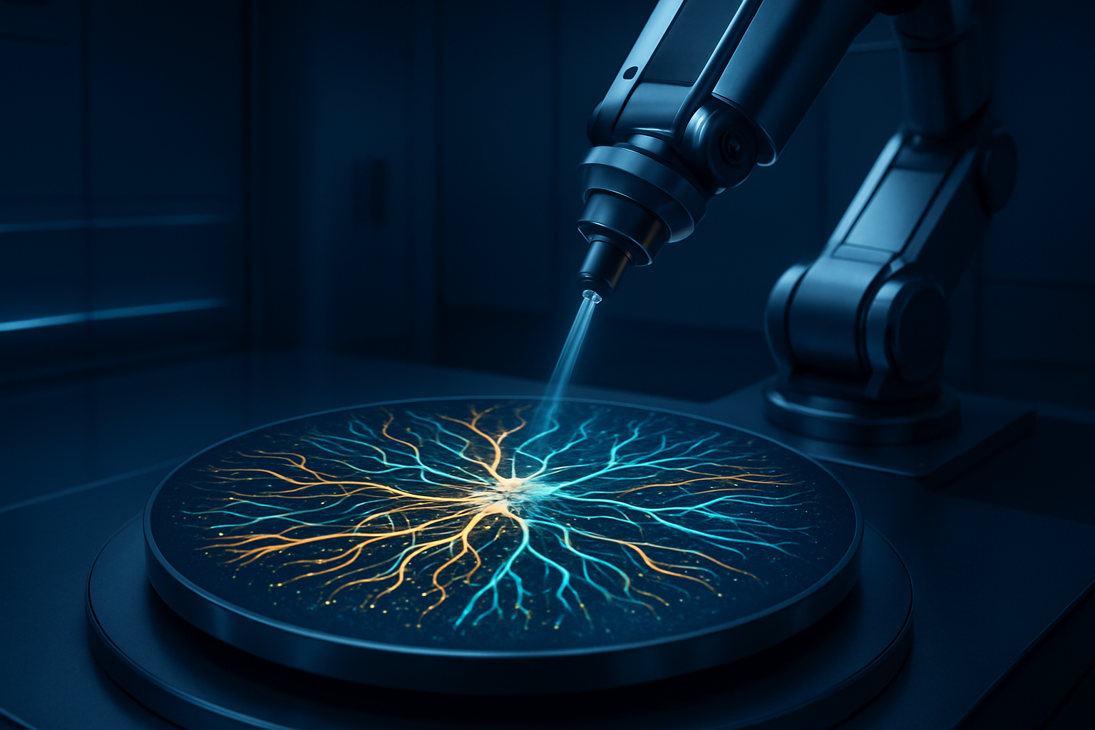
Author: mdierolf

  • The Silicon Frontier: Charting the Course for Next-Gen AI Hardware

    The Silicon Frontier: Charting the Course for Next-Gen AI Hardware

    The relentless march of artificial intelligence is pushing the boundaries of what's possible, but its ambitious future is increasingly contingent on a fundamental transformation in the very silicon that powers it. As AI models grow exponentially in complexity, demanding unprecedented computational power and energy efficiency, the industry stands at the precipice of a hardware revolution. The current paradigm, largely reliant on adapted general-purpose processors, is showing its limitations, paving the way for a new era of specialized semiconductors and architectural innovations designed from the ground up to unlock the full potential of next-generation AI.

    The immediate significance of this shift cannot be overstated. From the development of advanced multimodal AI capable of understanding and generating human-like content across various mediums, to agentic AI systems that make autonomous decisions, and physical AI driving robotics and autonomous vehicles, each leap forward hinges on foundational hardware advancements. The race is on to develop chips that are not just faster, but fundamentally more efficient, scalable, and capable of handling the diverse, complex, and real-time demands of an intelligent future.

    Beyond the Memory Wall: Architectural Innovations and Specialized Silicon

    The technical underpinnings of this hardware revolution are multifaceted, targeting the core inefficiencies and bottlenecks of current computing architectures. At the heart of the challenge lies the "memory wall" – a bottleneck inherent in the traditional Von Neumann architecture, where the constant movement of data between separate processing units and memory consumes significant energy and time. To overcome this, innovations are emerging on several fronts.

    One of the most promising architectural shifts is in-memory computing, or processing-in-memory (PIM), where computations are performed directly within or very close to the memory units. This drastically reduces the energy and latency associated with data transfer, a critical advantage for memory-intensive AI workloads like large language models (LLMs). Simultaneously, neuromorphic computing, inspired by the human brain's structure, seeks to mimic biological neural networks for highly energy-efficient and adaptive learning. These chips, like Intel's (NASDAQ: INTC) Loihi or IBM's (NYSE: IBM) NorthPole, promise a future of AI that learns and adapts with significantly less power.

    In terms of semiconductor technologies, the industry is exploring beyond traditional silicon. Photonic computing, which uses light instead of electrons for computation, offers the potential for orders of magnitude improvements in speed and energy efficiency for specific AI tasks like image recognition. Companies are developing light-powered chips that could achieve up to 100 times greater efficiency and faster processing. Furthermore, wide-bandgap (WBG) semiconductors like Gallium Nitride (GaN) and Silicon Carbide (SiC) are gaining traction for their superior power density and efficiency, making them ideal for high-power AI data centers and crucial for reducing the massive energy footprint of AI.

    These advancements represent a significant departure from previous approaches, which primarily focused on scaling up general-purpose GPUs. While GPUs, particularly those from Nvidia (NASDAQ: NVDA), have been the workhorses of the AI revolution due to their parallel processing capabilities, their general-purpose nature means they are not always optimally efficient for every AI task. The new wave of hardware is characterized by heterogeneous integration and chiplet architectures, where specialized components (CPUs, GPUs, NPUs, ASICs) are integrated within a single package, each optimized for specific parts of an AI workload. This modular approach, along with advanced packaging and 3D stacking, allows for greater flexibility, higher performance, and improved yields compared to monolithic chip designs. Initial reactions from the AI research community and industry experts are largely enthusiastic, recognizing these innovations as essential for sustaining the pace of AI progress and making it more sustainable. The consensus is that while general-purpose accelerators will remain important, specialized and integrated solutions are the key to unlocking the next generation of AI capabilities.

    The New Arms Race: Reshaping the AI Industry Landscape

    The emergence of these advanced AI hardware technologies is not merely an engineering feat; it's a strategic imperative that is profoundly reshaping the competitive landscape for AI companies, tech giants, and burgeoning startups. The ability to design, manufacture, or access cutting-edge AI silicon is becoming a primary differentiator, driving a new "arms race" in the technology sector.

    Tech giants with deep pockets and extensive R&D capabilities are at the forefront of this transformation. Companies like Nvidia (NASDAQ: NVDA) continue to dominate with their powerful GPUs and comprehensive software ecosystems, constantly innovating with new architectures like Blackwell. However, they face increasing competition from other behemoths. Google (NASDAQ: GOOGL) leverages its custom Tensor Processing Units (TPUs) to power its AI initiatives and cloud services, while Amazon (NASDAQ: AMZN) with AWS, and Microsoft (NASDAQ: MSFT) with Azure, are heavily investing in their own custom AI chips (like Amazon's Inferentia and Trainium, and Microsoft's Azure Maia 100) to optimize their cloud AI offerings. This vertical integration allows them to offer unparalleled performance and efficiency, attracting enterprises and reinforcing their market leadership. Intel (NASDAQ: INTC) is also making significant strides with its Gaudi AI accelerators and re-entering the foundry business to secure its position in this evolving market.

    The competitive implications are stark. The intensified competition is driving rapid innovation, but also leading to a diversification of hardware options, reducing dependency on a single supplier. "Hardware is strategic again" is a common refrain, as control over computing power becomes a critical component of national security and strategic influence. For startups, while the barrier to entry can be high due to the immense cost of developing cutting-edge chips, open-source hardware initiatives like RISC-V are democratizing access to customizable designs. This allows nimble startups to carve out niche markets, focusing on specialized AI hardware for edge computing or specific generative AI models. Companies like Groq, known for its ultra-fast inference chips, demonstrate the potential for startups to disrupt established players by focusing on specific, high-demand AI workloads.

    This shift also brings potential disruptions to existing products and services. General-purpose CPUs, while foundational, are becoming less suitable for sophisticated AI tasks, losing ground to specialized ASICs and GPUs. The rise of "AI PCs" equipped with Neural Processing Units (NPUs) signifies a move towards embedding AI capabilities directly into end-user devices, reducing reliance on cloud computing for some tasks, enhancing data privacy, and potentially "future-proofing" technology infrastructure. This evolution could shift some AI workloads from the cloud to the edge, creating new form factors and interfaces that prioritize AI-centric functionality. Ultimately, companies that can effectively integrate these new hardware paradigms into their products and services will gain significant strategic advantages, offering enhanced performance, greater energy efficiency, and the ability to enable real-time, sophisticated AI applications across diverse sectors.

    A New Era of Intelligence: Broader Implications and Looming Challenges

    The advancements in AI hardware and architectural innovations are not isolated technical achievements; they are the foundational bedrock upon which the next era of artificial intelligence will be built, fitting seamlessly into and accelerating broader AI trends. This symbiotic relationship between hardware and software is fueling the exponential growth of capabilities in areas like large language models (LLMs) and generative AI, which demand unprecedented computational power for both training and inference. The ability to process vast datasets and complex algorithms more efficiently is enabling AI to move beyond its current capabilities, facilitating advancements that promise more human-like reasoning and robust decision-making.

    A significant trend being driven by this hardware revolution is the proliferation of Edge AI. Specialized, low-power hardware is enabling AI to move from centralized cloud data centers to local devices – smartphones, autonomous vehicles, IoT sensors, and robotics. This shift allows for real-time processing, reduced latency, enhanced data privacy, and the deployment of AI in environments where constant cloud connectivity is impractical. The emergence of "AI PCs" equipped with Neural Processing Units (NPUs) is a testament to this trend, bringing sophisticated AI capabilities directly to the user's desktop, assisting with tasks and boosting productivity locally. These developments are not just about raw power; they are about making AI more ubiquitous, responsive, and integrated into our daily lives.

    However, this transformative progress is not without its significant challenges and concerns. Perhaps the most pressing is the energy consumption of AI. Training and running complex AI models, especially LLMs, consume enormous amounts of electricity. Projections suggest that data centers, heavily driven by AI workloads, could account for a substantial portion of global electricity use by 2030-2035, putting immense strain on power grids and contributing significantly to greenhouse gas emissions. The demand for water for cooling these vast data centers also presents an environmental concern. Furthermore, the cost of high-performance AI hardware remains prohibitive for many, creating an accessibility gap that concentrates cutting-edge AI development among a few large organizations. The rapid obsolescence of AI chips also contributes to a growing e-waste problem, adding another layer of environmental impact.

    Comparing this era to previous AI milestones highlights the unique nature of the current moment. The early AI era, relying on general-purpose CPUs, was largely constrained by computational limits. The GPU revolution, spearheaded by Nvidia (NASDAQ: NVDA) in the 2010s, unleashed parallel processing, leading to breakthroughs in deep learning. However, the current era, characterized by purpose-built AI chips (like Google's (NASDAQ: GOOGL) TPUs, ASICs, and NPUs) and radical architectural innovations like in-memory computing and neuromorphic designs, represents a leap in performance and efficiency that was previously unimaginable. Unlike past "AI winters," where expectations outpaced technological capabilities, today's hardware advancements provide the robust foundation for sustained software innovation, ensuring that the current surge in AI development is not just a fleeting trend but a fundamental shift towards a truly intelligent future.

    The Road Ahead: Near-Term Innovations and Distant Horizons

    The trajectory of AI hardware development points to a future of relentless innovation, driven by the insatiable computational demands of advanced AI models and the critical need for greater efficiency. In the near term, spanning late 2025 through 2027, the industry will witness an intensifying focus on custom AI silicon. Application-Specific Integrated Circuits (ASICs), Neural Processing Units (NPUs), and Tensor Processing Units (TPUs) will become even more prevalent, meticulously engineered for specific AI tasks to deliver superior speed, lower latency, and reduced energy consumption. While Nvidia (NASDAQ: NVDA) is expected to continue its dominance with new GPU architectures like Blackwell and the upcoming Rubin models, it faces growing competition. Qualcomm is launching new AI accelerator chips for data centers (AI200 in 2026, AI250 in 2027), optimized for inference, and AMD (NASDAQ: AMD) is strengthening its position with the MI350 series. Hyperscale cloud providers like Google (NASDAQ: GOOGL), Amazon (NASDAQ: AMZN), and Microsoft (NASDAQ: MSFT) are also deploying their own specialized silicon to reduce external reliance and offer optimized cloud AI services. Furthermore, advancements in High-Bandwidth Memory (HBM4) and interconnects like Compute Express Link (CXL) are crucial for overcoming memory bottlenecks and improving data transfer efficiency.

    Looking further ahead, beyond 2027, the landscape promises even more radical transformations. Neuromorphic computing, which aims to mimic the human brain's structure and function with highly efficient artificial synapses and neurons, is poised to deliver unprecedented energy efficiency and performance for tasks like pattern recognition. Companies like Intel (NASDAQ: INTC) with Loihi 2 and IBM (NYSE: IBM) with TrueNorth are at the forefront of this field, striving for AI systems that consume minimal energy while achieving powerful, brain-like intelligence. Even more distantly, Quantum AI hardware looms as a potentially revolutionary force. While still in early stages, the integration of quantum computing with AI could redefine computing by solving complex problems faster and more accurately than classical computers. Hybrid quantum-classical computing, where AI workloads utilize both quantum and classical machines, is an anticipated near-term step. The long-term vision also includes reconfigurable hardware that can dynamically adapt its architecture during AI execution, whether at the edge or in the cloud, to meet evolving algorithmic demands.

    These advancements will unlock a vast array of new applications. Real-time AI will become ubiquitous in autonomous vehicles, industrial robots, and critical decision-making systems. Edge AI will expand significantly, embedding sophisticated intelligence into smart homes, wearables, and IoT devices with enhanced privacy and reduced cloud dependence. The rise of Agentic AI, focused on autonomous decision-making, will enable companies to "employ" and train AI workers to integrate into hybrid human-AI teams, demanding low-power hardware optimized for natural language processing and perception. Physical AI will drive progress in robotics and autonomous systems, emphasizing embodiment and interaction with the physical world. In healthcare, agentic AI will lead to more sophisticated diagnostics and personalized treatments. However, significant challenges remain, including the high development costs of custom chips, the pervasive issue of energy consumption (with data centers projected to consume 20% of global electricity by 2025), hardware fragmentation, supply chain vulnerabilities, and the sheer architectural complexity of these new systems. Experts predict continued market expansion for AI chips, a diversification beyond GPU dominance, and a necessary rebalancing of investment towards AI infrastructure to truly unlock the technology's massive potential.

    The Foundation of Future Intelligence: A Comprehensive Wrap-Up

    The journey into the future of AI hardware reveals a landscape of profound transformation, where specialized silicon and innovative architectures are not just desirable but essential for the continued evolution of artificial intelligence. The key takeaway is clear: the era of relying solely on adapted general-purpose processors for advanced AI is rapidly drawing to a close. We are witnessing a fundamental shift towards purpose-built, highly efficient, and diverse computing solutions designed to meet the escalating demands of complex AI models, from massive LLMs to sophisticated agentic systems.

    This moment holds immense significance in AI history, akin to the GPU revolution that ignited the deep learning boom. However, it surpasses previous milestones by tackling the core inefficiencies of traditional computing head-on, particularly the "memory wall" and the unsustainable energy consumption of current AI. The long-term impact will be a world where AI is not only more powerful and intelligent but also more ubiquitous, responsive, and seamlessly integrated into every facet of society and industry. This includes the potential for AI to tackle global-scale challenges, from climate change to personalized medicine, driving an estimated $11.2 trillion market for AI models focused on business inference.

    In the coming weeks and months, several critical developments bear watching. Anticipate a flurry of new chip announcements and benchmarks from major players like Nvidia (NASDAQ: NVDA), AMD (NASDAQ: AMD), Intel (NASDAQ: INTC), Google (NASDAQ: GOOGL), Amazon (NASDAQ: AMZN), and Microsoft (NASDAQ: MSFT), particularly their performance on generative AI tasks. Keep an eye on strategic investments and partnerships aimed at securing critical compute power and expanding AI infrastructure. Monitor the progress in alternative architectures like neuromorphic and quantum computing, as any significant breakthroughs could signal major paradigm shifts. Geopolitical developments concerning export controls and domestic chip production will continue to shape the global supply chain. Finally, observe the increasing proliferation and capabilities of "AI PCs" and other edge devices, which will demonstrate the decentralization of AI processing, and watch for sustainability initiatives addressing the environmental footprint of AI. The future of AI is being forged in silicon, and its evolution will define the capabilities of intelligence itself.


    This content is intended for informational purposes only and represents analysis of current AI developments.

    TokenRing AI delivers enterprise-grade solutions for multi-agent AI workflow orchestration, AI-powered development tools, and seamless remote collaboration platforms.
    For more information, visit https://www.tokenring.ai/.

  • AI Chips Unleashed: The 2025 Revolution in Brain-Inspired Designs, Optical Speed, and Modular Manufacturing

    AI Chips Unleashed: The 2025 Revolution in Brain-Inspired Designs, Optical Speed, and Modular Manufacturing

    November 2025 marks an unprecedented surge in AI chip innovation, characterized by the commercialization of brain-like computing, a leap into light-speed processing, and a manufacturing paradigm shift towards modularity and AI-driven efficiency. These breakthroughs are immediately reshaping the technological landscape, driving sustainable, powerful AI from the cloud to the farthest edge of the network.

    The artificial intelligence hardware sector is currently undergoing a profound transformation, with significant advancements in both chip design and manufacturing processes directly addressing the escalating demands for performance, energy efficiency, and scalability. The immediate significance of these developments lies in their capacity to accelerate AI deployment across industries, drastically reduce its environmental footprint, and enable a new generation of intelligent applications that were previously out of reach due to computational or power constraints.

    Technical Deep Dive: The Engines of Tomorrow's AI

    The core of this revolution lies in several distinct yet interconnected technical advancements. Neuromorphic computing, which mimics the human brain's neural architecture, is finally moving beyond theoretical research into practical, commercial applications. Chips like Intel's (NASDAQ: INTC) Hala Point system, BrainChip's (ASX: BRN) Akida Pulsar, and Innatera's Spiking Neural Processor (SNP), have seen significant advancements or commercial launches in 2025. These systems are inherently energy-efficient, offering low-latency solutions ideal for edge AI, robotics, and the Internet of Things (IoT). For instance, Akida Pulsar boasts up to 500 times lower energy consumption and 100 times latency reduction compared to conventional AI cores for real-time, event-driven processing at the edge. Furthermore, USC researchers have demonstrated artificial neurons that replicate biological function with significantly reduced chip size and energy consumption, promising to advance artificial general intelligence. This paradigm shift directly addresses the critical need for sustainable AI by drastically cutting power usage in resource-constrained environments.

    Another major bottleneck in traditional computing architectures, the "memory wall," is being shattered by in-memory computing (IMC) and processing-in-memory (PIM) chips. These innovative designs perform computations directly within memory, dramatically reducing the movement of data between the processor and memory. This reduction in data transfer, in turn, slashes power consumption and significantly boosts processing speed. Companies like Qualcomm (NASDAQ: QCOM) are integrating near-memory computing into new solutions such as the AI250, providing a generational leap in effective memory bandwidth and efficiency specifically for AI inference workloads. This technology is crucial for managing the massive data processing demands of complex AI algorithms, enabling faster and more efficient training and inference for burgeoning generative AI models and large language models (LLMs).

    Perhaps one of the most futuristic developments is the emergence of optical computing. Scientists at Tsinghua University have achieved a significant milestone by developing a light-powered AI chip, OFE², capable of handling data at an unprecedented 12.5 GHz. This optical computing breakthrough completes complex pattern-recognition tasks by directing light beams through on-chip structures, consuming significantly less energy than traditional electronic devices. This innovation offers a potent solution to the growing energy demands of AI, potentially freeing AI from being a major contributor to global energy shortages. It promises a new generation of real-time, ultra-low-energy AI, crucial for sustainable and widespread deployment across various sectors.

    Finally, as traditional transistor scaling (often referred to as Moore's Law) faces physical limits, advanced packaging technologies and chiplet architectures have become paramount. Technologies like 2.5D and 3D stacking (e.g., CoWoS, 3DIC), Fan-Out Panel-Level Packaging (FO-PLP), and hybrid bonding are crucial for boosting performance, increasing integration density, improving signal integrity, and enhancing thermal management for AI chips. Complementing this, chiplet technology, which involves modularizing chip functions into discrete components, is gaining significant traction, with the Universal Chiplet Interconnect Express (UCIe) standard expanding its adoption. These innovations are the new frontier for hardware optimization, offering flexibility, cost-effectiveness, and faster development cycles. They also mitigate supply chain risks by allowing manufacturers to source different parts from multiple suppliers. The market for advanced packaging is projected to grow eightfold by 2033, underscoring its immediate importance for the widespread adoption of AI chips into consumer devices and automotive applications.

    Competitive Landscape: Winners and Disruptors

    These advancements are creating clear winners and potential disruptors within the AI industry. Chip designers and manufacturers at the forefront of these innovations stand to benefit immensely. Intel, with its neuromorphic Hala Point system, and BrainChip, with its Akida Pulsar, are well-positioned in the energy-efficient edge AI market. Qualcomm's integration of near-memory computing in its AI250 strengthens its leadership in mobile and edge AI processing. NVIDIA (NASDAQ: NVDA), while not explicitly mentioned for neuromorphic or optical chips, continues to dominate the high-performance computing space for AI training and is a key enabler for AI-driven manufacturing.

    The competitive implications are significant. Major AI labs and tech companies reliant on traditional architectures will face pressure to adapt or risk falling behind in performance and energy efficiency. Companies that can rapidly integrate these new chip designs into their products and services will gain a substantial strategic advantage. For instance, the ability to deploy AI models with significantly lower power consumption opens up new markets in battery-powered devices, remote sensing, and pervasive AI. The modularity offered by chiplets could also democratize chip design to some extent, allowing smaller players to combine specialized chiplets from various vendors to create custom, high-performance AI solutions, potentially disrupting the vertically integrated chip design model.

    Furthermore, AI's role in optimizing its own creation is a game-changer. AI-driven Electronic Design Automation (EDA) tools are dramatically accelerating chip design timelines—for example, reducing a 5nm chip's optimization cycle from six months to just six weeks. This means faster time-to-market for new AI chips, improved design quality, and more efficient, higher-yield manufacturing processes. Samsung (KRX: 005930), for instance, is establishing an "AI Megafactory" powered by 50,000 NVIDIA GPUs to revolutionize its chip production, integrating AI throughout its entire manufacturing flow. Similarly, SK Group is building an "AI factory" in South Korea with NVIDIA, focusing on next-generation memory and autonomous fab digital twins to optimize efficiency. These efforts are critical for meeting the skyrocketing demand for AI-optimized semiconductors and bolstering supply chain resilience amidst geopolitical shifts.

    Broader Significance: Shaping the AI Future

    These innovations fit perfectly into the broader AI landscape, addressing critical trends such as the insatiable demand for computational power for increasingly complex models (like LLMs), the push for sustainable and energy-efficient AI, and the proliferation of AI at the edge. The move towards neuromorphic and optical computing represents a fundamental shift away from the Von Neumann architecture, which has dominated computing for decades, towards more biologically inspired or physically optimized processing methods. This transition is not merely an incremental improvement but a foundational change that could unlock new capabilities in AI.

    The impacts are far-reaching. On one hand, these advancements promise more powerful, ubiquitous, and efficient AI, enabling breakthroughs in areas like personalized medicine, autonomous systems, and advanced scientific research. On the other hand, potential concerns, while mitigated by the focus on energy efficiency, still exist regarding the ethical implications of more powerful AI and the increasing complexity of hardware development. However, the current trajectory is largely positive, aiming to make AI more accessible and environmentally responsible.

    Comparing this to previous AI milestones, such as the rise of GPUs for deep learning or the development of specialized AI accelerators like Google's TPUs, these current advancements represent a diversification and deepening of the hardware foundation. While earlier milestones focused on brute-force parallelization, today's innovations are about architectural efficiency, novel physics, and self-optimization through AI, pushing beyond the limits of traditional silicon. This multi-pronged approach suggests a more robust and sustainable path for AI's continued growth.

    The Road Ahead: Future Developments and Challenges

    Looking to the near-term, we can expect to see further integration of these technologies. Hybrid chips combining neuromorphic, in-memory, and conventional processing units will likely become more common, optimizing specific workloads for maximum efficiency. The UCIe standard for chiplets will continue to gain traction, leading to a more modular and customizable AI hardware ecosystem. In the long-term, the full potential of optical computing, particularly in areas requiring ultra-high bandwidth and low latency, could revolutionize data centers and telecommunications infrastructure, creating entirely new classes of AI applications.

    Potential applications on the horizon include highly sophisticated, real-time edge AI for autonomous vehicles that can process vast sensor data with minimal latency and power, advanced robotics capable of learning and adapting in complex environments, and medical devices that can perform on-device diagnostics with unprecedented accuracy and speed. Generative AI and LLMs will also see significant performance boosts, enabling more complex and nuanced interactions, and potentially leading to more human-like AI capabilities.

    However, challenges remain. Scaling these nascent technologies to mass production while maintaining cost-effectiveness is a significant hurdle. The development of robust software ecosystems and programming models that can fully leverage the unique architectures of neuromorphic and optical chips will be crucial. Furthermore, ensuring interoperability between diverse chiplet designs and maintaining supply chain stability amidst global economic fluctuations will require continued innovation and international collaboration. Experts predict a continued convergence of hardware and software co-design, with AI playing an ever-increasing role in optimizing its own underlying infrastructure.

    A New Era for AI Hardware

    In summary, the latest innovations in AI chip design and manufacturing—encompassing neuromorphic computing, in-memory processing, optical chips, advanced packaging, and AI-driven manufacturing—represent a pivotal moment in the history of artificial intelligence. These breakthroughs are not merely incremental improvements but fundamental shifts that promise to make AI more powerful, energy-efficient, and ubiquitous than ever before.

    The significance of these developments cannot be overstated. They are addressing the core challenges of AI scalability and sustainability, paving the way for a future where AI is seamlessly integrated into every facet of our lives, from smart cities to personalized health. As we move forward, the interplay between novel chip architectures, advanced manufacturing techniques, and AI's self-optimizing capabilities will be critical to watch. The coming weeks and months will undoubtedly bring further announcements and demonstrations as companies race to capitalize on these transformative technologies, solidifying this period as a new era for AI hardware.


    This content is intended for informational purposes only and represents analysis of current AI developments.

    TokenRing AI delivers enterprise-grade solutions for multi-agent AI workflow orchestration, AI-powered development tools, and seamless remote collaboration platforms.
    For more information, visit https://www.tokenring.ai/.

  • Robotaxi Revolution Accelerates Demand for Advanced AI Chips, Waymo Leads the Charge

    Robotaxi Revolution Accelerates Demand for Advanced AI Chips, Waymo Leads the Charge

    The rapid expansion of autonomous vehicle technologies, spearheaded by industry leader Waymo (NASDAQ: GOOGL), is igniting an unprecedented surge in demand for advanced artificial intelligence chips. As Waymo aggressively scales its robotaxi services across new urban landscapes, the foundational hardware enabling these self-driving capabilities is undergoing a transformative evolution, pushing the boundaries of semiconductor innovation. This escalating need for powerful, efficient, and specialized AI processors is not merely a technological trend but a critical economic driver, reshaping the semiconductor industry, urban mobility, and the broader tech ecosystem.

    This growing reliance on cutting-edge silicon holds immediate and profound significance. It is accelerating research and development within the semiconductor sector, fostering critical supply chain dependencies, and playing a pivotal role in reducing the cost and increasing the accessibility of robotaxi services. Crucially, these advanced chips are the fundamental enablers for achieving higher levels of autonomy (Level 4 and Level 5), promising to redefine personal transportation, enhance safety, and improve traffic efficiency in cities worldwide. The expansion of Waymo's services, from Phoenix to new markets like Austin and Silicon Valley, underscores a tangible shift towards a future where autonomous vehicles are a daily reality, making the underlying AI compute power more vital than ever.

    The Silicon Brains: Unpacking the Technical Advancements Driving Autonomy

    The journey to Waymo-level autonomy, characterized by highly capable and safe self-driving systems, hinges on a new generation of AI chips that far surpass the capabilities of traditional processors. These specialized silicon brains are engineered to manage the immense computational load required for real-time sensor data processing, complex decision-making, and precise vehicle control.

    While Waymo develops its own custom "Waymo Gemini SoC" for onboard processing, focusing on sensor fusion and cloud-to-edge integration, the company also leverages high-performance GPUs for training its sophisticated AI models in data centers. Waymo's fifth-generation Driver, introduced in 2020, significantly upgraded its sensor suite, featuring high-resolution 360-degree lidar with over 300-meter range, high-dynamic-range cameras, and an imaging radar system, all of which demand robust and efficient compute. This integrated approach emphasizes redundant and robust perception across diverse environmental conditions, necessitating powerful, purpose-built AI acceleration.

    Other industry giants are also pushing the envelope. NVIDIA (NASDAQ: NVDA) with its DRIVE Thor superchip, is setting new benchmarks, capable of achieving up to 2,000 TOPS (Tera Operations Per Second) of FP8 performance. This represents a massive leap from its predecessor, DRIVE Orin (254 TOPS), by integrating Hopper GPU, Grace CPU, and Ada Lovelace GPU architectures. Thor's ability to consolidate multiple functions onto a single system-on-a-chip (SoC) reduces the need for numerous electronic control units (ECUs), improving efficiency and lowering system costs. It also incorporates the first inference transformer engine for AV platforms, accelerating deep neural networks crucial for modern AI workloads. Similarly, Mobileye (NASDAQ: INTC), with its EyeQ Ultra, offers 176 TOPS of AI acceleration on a single 5-nanometer SoC, claiming performance equivalent to ten EyeQ5 SoCs while significantly reducing power consumption. Qualcomm's (NASDAQ: QCOM) Snapdragon Ride Flex SoCs, built on 4nm process technology, are designed for scalable solutions, integrating digital cockpit and ADAS functions, capable of scaling to 2000 TOPS for fully automated driving with additional accelerators.

    These advancements represent a paradigm shift from previous approaches. Modern chips are moving towards consolidation and centralization, replacing distributed ECUs with highly integrated SoCs that simplify vehicle electronics and enable software-defined vehicles (SDVs). They incorporate specialized AI accelerators (NPUs, CNN clusters) for vastly more efficient processing of deep learning models, departing from reliance on general-purpose processors. Furthermore, the utilization of cutting-edge manufacturing processes (5nm, 4nm) allows for higher transistor density, boosting performance and energy efficiency, critical for managing the substantial power requirements of L4/L5 autonomy. Initial reactions from the AI research community highlight the convergence of automotive chip design with high-performance computing, emphasizing the critical need for efficiency, functional safety (ASIL-D compliance), and robust software-hardware co-design to tackle the complex challenges of real-world autonomous deployment.

    Corporate Battleground: Who Wins and Loses in the AI Chip Arms Race

    The escalating demand for advanced AI chips, fueled by the aggressive expansion of robotaxi services like Waymo's, is redrawing the competitive landscape across the tech and automotive industries. This silicon arms race is creating clear winners among semiconductor giants, while simultaneously posing significant challenges and opportunities for autonomous driving developers and related sectors.

    Chip manufacturers are undoubtedly the primary beneficiaries. NVIDIA (NASDAQ: NVDA), with its powerful DRIVE AGX Orin and the upcoming DRIVE Thor superchip, capable of up to 2,000 TOPS, maintains a dominant position, leveraging its robust software-hardware integration and extensive developer ecosystem. Intel (NASDAQ: INTC), through its Mobileye subsidiary, is another key player, with its EyeQ SoCs embedded in numerous vehicles. Qualcomm (NASDAQ: QCOM) is also making aggressive strides with its Snapdragon Ride platforms, partnering with major automakers like BMW. Beyond these giants, specialized AI chip designers like Ambarella, along with traditional automotive chip suppliers such as NXP Semiconductors (NASDAQ: NXPI) and Infineon Technologies (ETR: IFX), are all seeing increased demand for their diverse range of automotive-grade silicon. Memory chip manufacturers like Micron Technology (NASDAQ: MU) also stand to gain from the exponential data processing needs of autonomous vehicles.

    For autonomous driving companies, the implications are profound. Waymo (NASDAQ: GOOGL), as a pioneer, benefits from its deep R&D resources and extensive real-world driving data, which is invaluable for training its "Waymo Foundation Model" – an innovative blend of AV and generative AI concepts. However, its reliance on cutting-edge hardware also means significant capital expenditure. Companies like Tesla (NASDAQ: TSLA), Cruise (NYSE: GM), and Zoox (NASDAQ: AMZN) are similarly reliant on advanced AI chips, with Tesla notably pursuing vertical integration by designing its own FSD and Dojo chips to optimize performance and reduce dependency on third-party suppliers. This trend of in-house chip development by major tech and automotive players signals a strategic shift, allowing for greater customization and performance optimization, albeit at substantial investment and risk.

    The disruption extends far beyond direct chip and AV companies. Traditional automotive manufacturing faces a fundamental transformation, shifting focus from mechanical components to advanced electronics and software-defined architectures. Cloud computing providers like Google Cloud and Amazon Web Services (AWS) are becoming indispensable for managing vast datasets, training AI algorithms, and delivering over-the-air updates for autonomous fleets. The insurance industry, too, is bracing for significant disruption, with potential losses estimated at billions by 2035 due to the anticipated reduction in human-error-induced accidents, necessitating new models focused on cybersecurity and software liability. Furthermore, the rise of robotaxi services could fundamentally alter car ownership models, favoring on-demand mobility over personal vehicles, and revolutionizing logistics and freight transportation. However, this also raises concerns about job displacement in traditional driving and manufacturing sectors, demanding significant workforce retraining initiatives.

    In this fiercely competitive landscape, companies are strategically positioning themselves through various means. A relentless pursuit of higher performance (TOPS) coupled with greater energy efficiency is paramount, driving innovation in specialized chip architectures. Companies like NVIDIA offer comprehensive full-stack solutions, encompassing hardware, software, and development ecosystems, to attract automakers. Those with access to vast real-world driving data, such as Waymo and Tesla, possess a distinct advantage in refining their AI models. The move towards software-defined vehicle architectures, enabling flexibility and continuous improvement through OTA updates, is also a key differentiator. Ultimately, safety and reliability, backed by rigorous testing and adherence to emerging regulatory frameworks, will be the ultimate determinants of success in this rapidly evolving market.

    Beyond the Road: The Wider Significance of the Autonomous Chip Boom

    The increasing demand for advanced AI chips, propelled by the relentless expansion of robotaxi services like Waymo's, signifies a critical juncture in the broader AI landscape. This isn't just about faster cars; it's about the maturation of edge AI, the redefinition of urban infrastructure, and a reckoning with profound societal shifts. This trend fits squarely into the "AI supercycle," where specialized AI chips are paramount for real-time, low-latency processing at the data source – in this case, within the autonomous vehicle itself.

    The societal impacts promise a future of enhanced safety and mobility. Autonomous vehicles are projected to drastically reduce traffic accidents by eliminating human error, offering a lifeline of independence to those unable to drive. Their integration with 5G and Vehicle-to-Everything (V2X) communication will be a cornerstone of smart cities, optimizing traffic flow and urban planning. Economically, the market for automotive AI is projected to soar, fostering new business models in ride-hailing and logistics, and potentially improving overall productivity by streamlining transport. Environmentally, AVs, especially when coupled with electric vehicle technology, hold the potential to significantly reduce greenhouse gas emissions through optimized driving patterns and reduced congestion.

    However, this transformative shift is not without its concerns. Ethical dilemmas are at the forefront, particularly in unavoidable accident scenarios where AI systems must make life-or-death decisions, raising complex moral and legal questions about accountability and algorithmic bias. The specter of job displacement looms large over the transportation sector, from truck drivers to taxi operators, necessitating proactive retraining and upskilling initiatives. Safety remains paramount, with public trust hinging on the rigorous testing and robust security of these systems against hacking vulnerabilities. Privacy is another critical concern, as connected AVs generate vast amounts of personal and behavioral data, demanding stringent data protection and transparent usage policies.

    Comparing this moment to previous AI milestones reveals its unique significance. While early AI focused on rule-based systems and brute-force computation (like Deep Blue's chess victory), and the DARPA Grand Challenges in the mid-2000s demonstrated rudimentary autonomous capabilities, today's advancements are fundamentally different. Powered by deep learning models, massive datasets, and specialized AI hardware, autonomous vehicles can now process complex sensory input in real-time, perceive nuanced environmental factors, and make highly adaptive decisions – capabilities far beyond earlier systems. The shift towards Level 4 and Level 5 autonomy, driven by increasingly powerful and reliable AI chips, marks a new frontier, solidifying this period as a critical phase in the AI supercycle, moving from theoretical possibility to tangible, widespread deployment.

    The Road Ahead: Future Developments in Autonomous AI Chips

    The trajectory of advanced AI chips, propelled by the relentless expansion of autonomous vehicle technologies and robotaxi services like Waymo's, points towards a future of unprecedented innovation and transformative applications. Near-term developments, spanning the next five years (2025-2030), will see the rapid proliferation of edge AI, with specialized SoCs and Neural Processing Units (NPUs) enabling powerful, low-latency inference directly within vehicles. Companies like NVIDIA (NASDAQ: NVDA), Qualcomm (NASDAQ: QCOM), and Intel (NASDAQ: INTC) /Mobileye will continue to push the boundaries of processing power, with chips like NVIDIA's Drive Thor and Qualcomm's Snapdragon Ride Flex becoming standard in high-end autonomous systems. The widespread adoption of Software-Defined Vehicles (SDVs) will enable continuous over-the-air updates, enhancing vehicle adaptability and functionality. Furthermore, the integration of 5G connectivity will be crucial for Vehicle-to-Everything (V2X) communication, fostering ultra-fast data exchange between vehicles and infrastructure, while energy-efficient designs remain a paramount focus to extend the range of electric autonomous vehicles.

    Looking further ahead, beyond 2030, the long-term evolution of AI chips will be characterized by even more advanced architectures, including highly energy-efficient NPUs and the exploration of neuromorphic computing, which mimics the human brain's structure for superior in-vehicle AI. This continuous push for exponential computing power, reliability, and redundancy will be essential for achieving full Level 4 and Level 5 autonomous driving, capable of handling complex and unpredictable scenarios without human intervention. These adaptable hardware designs, leveraging advanced process nodes like 4nm and 3nm, will provide the necessary performance headroom for increasingly sophisticated AI algorithms and predictive maintenance capabilities, allowing autonomous fleets to self-monitor and optimize performance.

    The potential applications and use cases on the horizon are vast. Fully autonomous robotaxi services, expanding beyond Waymo's current footprint, will provide widespread on-demand driverless transportation. AI will enable hyper-personalized in-car experiences, from intelligent voice assistants to adaptive cabin environments. Beyond passenger transport, autonomous vehicles with advanced AI chips will revolutionize logistics through driverless trucks and significantly contribute to smart city initiatives by improving traffic flow, safety, and parking management via V2X communication. Enhanced sensor fusion and perception, powered by these chips, will create a comprehensive real-time understanding of the vehicle's surroundings, leading to superior object detection and obstacle avoidance.

    However, significant challenges remain. The high manufacturing costs of these complex AI-driven chips and advanced SoCs necessitate cost-effective production solutions. The automotive industry must also build more resilient and diversified semiconductor supply chains to mitigate global shortages. Cybersecurity risks will escalate as vehicles become more connected, demanding robust security measures. Evolving regulatory compliance and the need for harmonized international standards are critical for global market expansion. Furthermore, the high power consumption and thermal management of advanced autonomous systems pose engineering hurdles, requiring efficient heat dissipation and potentially dedicated power sources. Experts predict that the automotive semiconductor market will reach between $129 billion and $132 billion by 2030, with AI chips within this segment experiencing a nearly 43% CAGR through 2034. Fully autonomous cars could comprise up to 15% of passenger vehicles sold worldwide by 2030, potentially rising to 80% by 2040, depending on technological advancements, regulatory frameworks, and consumer acceptance. The consensus is clear: the automotive industry, powered by specialized semiconductors, is on a trajectory to transform vehicles into sophisticated, evolving intelligent systems.

    Conclusion: Driving into an Autonomous Future

    The journey towards widespread autonomous mobility, powerfully driven by Waymo's (NASDAQ: GOOGL) ambitious robotaxi expansion, is inextricably linked to the relentless innovation in advanced AI chips. These specialized silicon brains are not merely components; they are the fundamental enablers of a future where vehicles perceive, decide, and act with unprecedented precision and safety. The automotive AI chip market, projected for explosive growth, underscores the criticality of this hardware in bringing Level 4 and Level 5 autonomy from research labs to public roads.

    This development marks a pivotal moment in AI history. It signifies the tangible deployment of highly sophisticated AI in safety-critical, real-world applications, moving beyond theoretical concepts to mainstream services. The increasing regulatory trust, as evidenced by decisions from bodies like the NHTSA regarding Waymo, further solidifies AI's role as a reliable and transformative force in transportation. The long-term impact promises a profound reshaping of society: safer roads, enhanced mobility for all, more efficient urban environments, and significant economic shifts driven by new business models and strategic partnerships across the tech and automotive sectors.

    As we navigate the coming weeks and months, several key indicators will illuminate the path forward. Keep a close watch on Waymo's continued commercial rollouts in new cities like Washington D.C., Atlanta, and Miami, and its integration of 6th-generation Waymo Driver technology into new vehicle platforms. The evolving competitive landscape, with players like Uber (NYSE: UBER) rolling out their own robotaxi services, will intensify the race for market dominance. Crucially, monitor the ongoing advancements in energy-efficient AI processors and the emergence of novel computing paradigms like neuromorphic chips, which will be vital for scaling autonomous capabilities. Finally, pay attention to the development of harmonized regulatory standards and ethical frameworks, as these will be essential for building public trust and ensuring the responsible deployment of this revolutionary technology. The convergence of advanced AI chips and autonomous vehicle technology is not just an incremental improvement but a fundamental shift that promises to reshape society. The groundwork laid by pioneers like Waymo, coupled with the relentless innovation in semiconductor technology, positions us on the cusp of an era where intelligent, self-driving systems become an integral part of our daily lives.


    This content is intended for informational purposes only and represents analysis of current AI developments.

    TokenRing AI delivers enterprise-grade solutions for multi-agent AI workflow orchestration, AI-powered development tools, and seamless remote collaboration platforms.
    For more information, visit https://www.tokenring.ai/.

  • Nvidia’s Arizona Gambit: Forging America’s AI Future with Domestic Chip Production

    Nvidia’s Arizona Gambit: Forging America’s AI Future with Domestic Chip Production

    Nvidia's (NASDAQ: NVDA) strategic pivot towards localizing the production of its cutting-edge artificial intelligence (AI) chips within the United States, particularly through significant investments in Arizona, marks a watershed moment in the global technology landscape. This bold initiative, driven by a confluence of surging AI demand, national security imperatives, and a push for supply chain resilience, aims to solidify America's leadership in the AI era. The immediate significance of this move is profound, establishing a robust domestic infrastructure for the "engines of the world's AI," thereby mitigating geopolitical risks and fostering an accelerated pace of innovation on U.S. soil.

    This strategic shift is a direct response to global calls for re-industrialization and a reduction in reliance on concentrated overseas manufacturing. By bringing the production of its most advanced AI processors, including the powerful Blackwell architecture, to U.S. facilities, Nvidia is not merely expanding its manufacturing footprint but actively reshaping the future of AI development and the stability of the critical AI chip supply chain. This commitment, underscored by substantial financial investment and extensive partnerships, positions the U.S. at the forefront of the burgeoning AI industrial revolution.

    Engineering the Future: Blackwell Chips and the Arizona Production Hub

    Nvidia's most powerful AI chip architecture, Blackwell, is now in full volume production at Taiwan Semiconductor Manufacturing Company's (NYSE: TSM) facilities in Phoenix, Arizona. This represents a historic departure from manufacturing these cutting-edge chips exclusively in Taiwan, with Nvidia CEO Jensen Huang heralding it as the first time the "engines of the world's AI infrastructure are being built in the United States." This advanced production leverages TSMC's capabilities to produce sophisticated 4-nanometer and 5-nanometer chips, with plans to advance to 3-nanometer, 2-nanometer, and even A16 technologies in the coming years.

    The Blackwell architecture itself is a marvel of engineering, with flagship products like the Blackwell Ultra designed to deliver up to 15 petaflops of performance for demanding AI workloads, each chip packing an astonishing 208 billion transistors. These chips feature an enhanced Transformer Engine optimized for large language models and a new Decompression Engine to accelerate database queries, representing a significant leap over their Hopper predecessors. Beyond wafer fabrication, Nvidia has forged critical partnerships for advanced packaging and testing operations in Arizona with companies like Amkor (NASDAQ: AMKR) and SPIL, utilizing complex chip-on-wafer-on-substrate (CoWoS) technology, specifically CoWoS-L, for its Blackwell chips.

    This approach differs significantly from previous strategies that heavily relied on a centralized, often overseas, manufacturing model. By diversifying its supply chain and establishing an integrated U.S. ecosystem—from fabrication in Arizona to packaging and testing in Arizona, and supercomputer assembly in Texas with partners like Foxconn (TWSE: 2317) and Wistron (TWSE: 3231)—Nvidia is building a more resilient and secure supply chain. While initial fabrication is moving to the U.S., a crucial aspect of high-end AI chip production, advanced packaging, still largely depends on facilities in Taiwan, though Amkor's upcoming Arizona plant by 2027-2028 aims to localize this critical process.

    Initial reactions from the AI research community and industry experts have been overwhelmingly positive, viewing Nvidia's technical pivot to U.S. production as a crucial step towards a more robust and secure AI infrastructure. Experts commend the move for strengthening the U.S. semiconductor supply chain and securing America's leadership in artificial intelligence, acknowledging the strategic importance of mitigating geopolitical risks. While acknowledging the higher manufacturing costs in the U.S. compared to Taiwan, the national security and supply chain benefits are widely considered paramount.

    Reshaping the AI Ecosystem: Implications for Companies and Competitive Dynamics

    Nvidia's aggressive push for AI chip production in the U.S. is poised to significantly reshape the competitive landscape for AI companies, tech giants, and startups. Domestically, U.S.-based AI labs, cloud providers, and startups stand to benefit immensely from faster and more reliable access to Nvidia's cutting-edge hardware. This localized supply chain can accelerate innovation cycles, reduce lead times, and provide a strategic advantage in developing and deploying next-generation AI solutions. Major American tech giants like Google (NASDAQ: GOOGL), Microsoft (NASDAQ: MSFT), Meta (NASDAQ: META), and Oracle (NYSE: ORCL), all significant customers of Nvidia's advanced chips, will benefit from enhanced supply chain resilience and potentially quicker access to the foundational hardware powering their vast AI initiatives.

    However, the implications extend beyond domestic advantages. Nvidia's U.S. production strategy, coupled with export restrictions on its most advanced chips to certain regions like China, creates a growing disparity in AI computing power globally. Non-U.S. companies in restricted regions may face significant limitations in acquiring top-tier Nvidia hardware, compelling them to invest more heavily in indigenous chip development or seek alternative suppliers. This could lead to a fragmented global AI landscape, where access to the most advanced hardware becomes a strategic national asset.

    The move also has potential disruptive effects on existing products and services. While it significantly strengthens supply chain resilience, the higher manufacturing costs in the U.S. could translate to increased prices for AI infrastructure and services, potentially impacting profit margins or being passed on to end-users. Conversely, the accelerated AI innovation within the U.S. due to enhanced hardware access could lead to the faster development and deployment of new AI products and services by American companies, potentially disrupting global market dynamics and establishing new industry standards.

    Nvidia's market positioning is further solidified by this strategy. It is positioning itself not just as a chip supplier but as a critical infrastructure partner for governments and major industries. By securing a domestic supply of its most advanced AI chips, Nvidia reinforces its technological leadership and aligns with U.S. policy goals of re-industrializing and maintaining a technological edge. This enhanced control over the domestic "AI technology stack" provides a unique competitive advantage, enabling closer integration and optimization of hardware and software, and propelling Nvidia's market valuation to an unprecedented $5 trillion.

    A New Industrial Revolution: Wider Significance and Geopolitical Chess

    Nvidia's U.S. AI chip production strategy is not merely an expansion of manufacturing; it's a foundational element of the broader AI landscape and an indicator of significant global trends. These chips are the "engines" powering the generative AI revolution, large language models, high-performance computing, robotics, and autonomous systems across every conceivable industry. The establishment of "AI factories"—data centers specifically designed for AI processing—underscores the profound shift towards AI as a core industrial infrastructure, driving what many are calling a new industrial revolution.

    The economic impacts are projected to be immense. Nvidia's commitment to produce up to $500 billion in AI infrastructure in the U.S. over the next four years is expected to create hundreds of thousands, if not millions, of high-quality jobs and generate trillions of dollars in economic activity. This strengthens the U.S. semiconductor industry and ensures its capacity to meet the surging global demand for AI technologies, reinforcing the "Made in America" agenda.

    Geopolitically, this move is a strategic chess piece. It aims to enhance supply chain resilience and reduce reliance on Asian production, particularly Taiwan, amidst escalating trade tensions and the ongoing technological rivalry with China. U.S. government incentives, such as the CHIPS and Science Act, and direct pressure have influenced this shift, with the goal of maintaining American technological dominance. However, U.S. export controls on advanced AI chips to China have created a complex "AI Cold War," impacting Nvidia's revenue from the Chinese market and intensifying the global race for AI supremacy.

    Potential concerns include the higher cost of manufacturing in the U.S., though Nvidia anticipates improved efficiency over time. More broadly, Nvidia's near-monopoly in high-performance AI chips has raised concerns about market concentration and potential anti-competitive practices, leading to antitrust scrutiny. The U.S. policy of reserving advanced AI chips for American companies and allies, while limiting access for rivals, also raises questions about global equity in AI development and could exacerbate the technological divide. This era is often compared to a new "industrial revolution," with Nvidia's rise built on decades of foresight in recognizing the power of GPUs for parallel computing, a bet that now underpins the pervasive industrial and economic integration of AI.

    The Road Ahead: Future Developments and Expert Predictions

    Nvidia's strategic expansion in the U.S. is a long-term commitment. In the near term, the focus will be on the full ramp-up of Blackwell chip production in Arizona and the operationalization of AI supercomputer manufacturing plants in Texas, with mass production expected in the next 12-15 months. Nvidia also unveiled its next-generation AI chip, "Vera Rubin" (or "Rubin"), at the GTC conference in October 2025, with Rubin GPUs slated for mass production in late 2026. This continuous innovation in chip architecture, coupled with localized production, will further cement the U.S.'s role as a hub for advanced AI hardware.

    These U.S.-produced AI chips and supercomputers are poised to be the "engines" for a new era of "AI factories," driving an "industrial revolution" across every sector. Potential applications include accelerating machine learning and deep learning processes, revolutionizing big data analytics, boosting AI capabilities in edge devices, and enabling the development of "physical AI" through digital twins and advanced robotics. Nvidia's partnerships with robotics companies like Figure also highlight its commitment to advancing next-generation humanoid robotics.

    However, significant challenges remain. The higher cost of domestic manufacturing is a persistent concern, though Nvidia views it as a necessary investment for national security and supply chain resilience. A crucial challenge is addressing the skilled labor shortage in advanced semiconductor manufacturing, packaging, and testing, even with Nvidia's plans for automation and robotics. Geopolitical shifts and export controls, particularly concerning China, continue to pose significant hurdles, with the U.S. government's stringent restrictions prompting Nvidia to develop region-specific products and navigate a complex regulatory landscape. Experts predict that these restrictions will compel China to further accelerate its indigenous AI chip development.

    Experts foresee that Nvidia's strategy will create hundreds of thousands, potentially millions, of high-quality jobs and drive trillions of dollars in economic security in the U.S. The decision to keep the most powerful AI chips primarily within the U.S. is seen as a pivotal moment for national competitive strength in AI. Nvidia is expected to continue its strategy of deep vertical integration, co-designing hardware and software across the entire stack, and expanding into areas like quantum computing and advanced telecommunications. Industry leaders also urge policymakers to strike a balance with export controls to safeguard national security without stifling innovation.

    A Defining Era: Wrap-Up and What to Watch For

    Nvidia's transformative strategy for AI chip production in the United States, particularly its deep engagement in Arizona, represents a historic milestone in U.S. manufacturing and a defining moment in AI history. By bringing the fabrication of its most advanced Blackwell AI chips to TSMC's facilities in Phoenix and establishing a comprehensive domestic ecosystem for supercomputer assembly and advanced packaging, Nvidia is actively re-industrializing the nation and fortifying its critical AI supply chain. The company's commitment of up to $500 billion in U.S. AI infrastructure underscores the profound economic and strategic benefits anticipated, including massive job creation and trillions in economic security.

    This development signifies a robust comeback for America in advanced semiconductor fabrication, cementing its role as a preeminent force in AI hardware development and significantly reducing reliance on Asian manufacturing amidst escalating geopolitical tensions. The U.S. government's proactive stance in prioritizing domestic production, coupled with policies to reserve advanced chips for American companies, carries profound national security implications, aiming to safeguard technological leadership in what is increasingly being termed the "AI industrial revolution."

    In the long term, this strategy is expected to yield substantial economic and strategic advantages for the U.S., accelerating AI innovation and infrastructure development domestically. However, the path forward is not without challenges, including the higher costs of U.S. manufacturing, the imperative to cultivate a skilled workforce, and the complex geopolitical landscape shaped by export restrictions and technological rivalries, particularly with China. The fragmentation of global supply chains and the intensification of the race for technological sovereignty will be defining features of this era.

    In the coming weeks and months, several key developments warrant close attention. Watch for further clarifications from the Commerce Department regarding "advanced" versus "downgraded" chip definitions, which will dictate global access to Nvidia's products. The operational ramp-up of Nvidia's supercomputer manufacturing plants in Texas will be a significant indicator of progress. Crucially, the completion and operationalization of Amkor's $2 billion packaging facility in Arizona by 2027-2028 will be pivotal, enabling full CoWoS packaging capabilities in the U.S. and further reducing reliance on Taiwan. The evolving competitive landscape, with other tech giants pursuing their own AI chip designs, and the broader geopolitical implications of these protectionist measures on international trade will continue to unfold, shaping the future of AI globally.


    This content is intended for informational purposes only and represents analysis of current AI developments.

    TokenRing AI delivers enterprise-grade solutions for multi-agent AI workflow orchestration, AI-powered development tools, and seamless remote collaboration platforms.
    For more information, visit https://www.tokenring.ai/.

  • TSMC’s Arizona Bet: Forging America’s AI Chip Future with Unprecedented Investment

    TSMC’s Arizona Bet: Forging America’s AI Chip Future with Unprecedented Investment

    Phoenix, AZ – November 3, 2025 – Taiwan Semiconductor Manufacturing Company (TSMC) (NYSE: TSM) is dramatically reshaping the landscape of advanced semiconductor manufacturing in the United States, cementing its pivotal role in bolstering American capabilities, particularly in the burgeoning field of artificial intelligence. With an unprecedented commitment now reaching US$165 billion, TSMC's expanded investment in Arizona signifies a monumental strategic shift, aiming to establish a robust, end-to-end domestic supply chain for cutting-edge AI chips. This move is not merely an expansion; it's a foundational build-out designed to secure U.S. leadership in AI, enhance national security through supply chain resilience, and create tens of thousands of high-tech jobs.

    This aggressive push by the world's leading contract chipmaker comes at a critical juncture, as global demand for advanced AI accelerators continues to skyrocket. The immediate significance of TSMC's U.S. endeavor is multi-faceted: it promises to bring the most advanced chip manufacturing processes, including 3-nanometer (N3) and 2-nanometer (N2) technologies, directly to American soil. This onshoring effort, heavily supported by the U.S. government's CHIPS and Science Act, aims to reduce geopolitical risks, shorten lead times for critical components, and foster a vibrant domestic ecosystem capable of supporting the next generation of AI innovation. The recent celebration of the first NVIDIA (NASDAQ: NVDA) Blackwell wafer produced on U.S. soil at TSMC's Phoenix facility in October 2025 underscored this milestone, signaling a new era of domestic advanced AI chip production.

    A New Era of Domestic Advanced Chipmaking: Technical Prowess Takes Root in Arizona

    TSMC's expanded Arizona complex is rapidly evolving into a cornerstone of U.S. advanced semiconductor manufacturing, poised to deliver unparalleled technical capabilities crucial for the AI revolution. The initial investment has blossomed into a three-fab strategy, complemented by plans for advanced packaging facilities and a significant research and development center, all designed to create a comprehensive domestic AI supply chain. This represents a stark departure from previous reliance on overseas fabrication, bringing the most sophisticated processes directly to American shores.

    The first fab at TSMC Arizona commenced high-volume production of 4-nanometer (N4) process technology in late 2024, a significant step that immediately elevated the U.S.'s domestic advanced chipmaking capacity. Building on this, the structure for the second fab was completed in 2025 and is targeted to begin volume production of 3-nanometer (N3) technology in 2028, with plans to produce the world's most advanced 2-nanometer (N2) process technology. Furthermore, TSMC broke ground on a third fab in April 2025, which is projected to produce chips using 2nm or even more advanced processes, such as A16, with production expected to begin by the end of the decade. Each of these advanced fabs is designed with cleanroom areas approximately double the size of an industry-standard logic fab, reflecting the scale and complexity of modern chip manufacturing.

    This domestic manufacturing capability is a game-changer for AI chip design. Companies like NVIDIA (NASDAQ: NVDA), a key TSMC partner, rely heavily on these leading-edge process technologies to pack billions of transistors onto their graphics processing units (GPUs) and AI accelerators. The N3 and N2 nodes offer significant improvements in transistor density, power efficiency, and performance over previous generations, directly translating to more powerful and efficient AI models. This differs from previous approaches where such advanced fabrication was almost exclusively concentrated in Taiwan, introducing potential logistical and geopolitical vulnerabilities. The onshoring of these capabilities means closer collaboration between U.S.-based chip designers and manufacturers, potentially accelerating innovation cycles and streamlining supply chains.

    Initial reactions from the AI research community and industry experts have been overwhelmingly positive, albeit with a pragmatic understanding of the challenges involved. The ability to source cutting-edge AI chips domestically is seen as a critical enabler for national AI strategies and a safeguard against supply chain disruptions. Experts highlight that while the upfront costs and complexities of establishing such facilities are immense, the long-term strategic advantages in terms of innovation, security, and economic growth far outweigh them. The U.S. government's substantial financial incentives through the CHIPS Act, including up to US$6.6 billion in direct funding and US$5 billion in loans, underscore the national importance of this endeavor.

    Reshaping the AI Industry Landscape: Beneficiaries and Competitive Shifts

    TSMC's burgeoning U.S. advanced manufacturing footprint is poised to profoundly impact the competitive dynamics within the artificial intelligence industry, creating clear beneficiaries and potentially disrupting existing market positions. The direct availability of cutting-edge fabrication on American soil will provide strategic advantages to companies heavily invested in AI hardware, while also influencing the broader tech ecosystem.

    Foremost among the beneficiaries are U.S.-based AI chip design powerhouses such as NVIDIA (NASDAQ: NVDA), Advanced Micro Devices (NASDAQ: AMD), Apple (NASDAQ: AAPL), Broadcom (NASDAQ: AVGO), and Qualcomm (NASDAQ: QCOM). These companies are TSMC's largest customers and rely on its advanced process technologies to bring their innovative AI accelerators, CPUs, and specialized chips to market. Having a domestic source for their most critical components reduces logistical complexities, shortens supply chains, and mitigates risks associated with geopolitical tensions, particularly concerning the Taiwan Strait. For NVIDIA, whose Blackwell platform chips are now being produced on U.S. soil at TSMC Arizona, this means a more resilient and potentially faster pathway to deliver the hardware powering the next generation of AI.

    The competitive implications for major AI labs and tech companies are significant. Access to advanced, domestically produced chips can accelerate the development and deployment of new AI models and applications. Companies that can quickly iterate and scale their hardware will gain a competitive edge in the race for AI dominance. This could also indirectly benefit cloud service providers like Amazon (NASDAQ: AMZN) AWS, Microsoft (NASDAQ: MSFT) Azure, and Google (NASDAQ: GOOGL) Cloud, who are heavily investing in AI infrastructure and custom silicon, by providing them with a more secure and diversified supply of high-performance chips.

    Potential disruption to existing products or services could arise from increased competition and faster innovation cycles. As more advanced chips become readily available, companies might be able to offer more powerful AI-driven features, potentially rendering older hardware or less optimized services less competitive. Furthermore, this move could bolster the efforts of Intel (NASDAQ: INTC) Foundry Services, which is also aggressively pursuing advanced manufacturing in the U.S. While TSMC and Intel are competitors in the foundry space, TSMC's presence helps to build out the overall U.S. supply chain ecosystem, from materials to equipment, which could indirectly benefit all domestic manufacturers.

    In terms of market positioning and strategic advantages, TSMC's U.S. expansion solidifies its role as an indispensable partner for American tech giants. It allows these companies to claim "Made in USA" for critical AI components, a powerful marketing and strategic advantage in an era focused on national industrial capabilities. This strategic alignment between TSMC and its U.S. customers strengthens the entire American technology sector, positioning it for sustained leadership in the global AI race.

    Wider Significance: Anchoring America's AI Future and Global Semiconductor Rebalancing

    TSMC's ambitious expansion in the United States transcends mere manufacturing; it represents a profound rebalancing act within the global semiconductor landscape and a critical anchor for America's long-term AI strategy. This initiative fits squarely into the broader trend of nations seeking to secure their technology supply chains and foster domestic innovation, particularly in strategic sectors like AI.

    The impacts of this development are far-reaching. Geopolitically, it significantly de-risks the global technology supply chain by diversifying advanced chip production away from a single region. The concentration of cutting-edge fabrication in Taiwan has long been a point of vulnerability, and TSMC's U.S. fabs offer a crucial layer of resilience against potential disruptions, whether from natural disasters or geopolitical tensions. This move directly supports the U.S. government's push for "chip sovereignty," a national security imperative aimed at ensuring access to the most advanced semiconductors for defense, economic competitiveness, and AI leadership.

    Economically, the investment is a massive boon, projected to generate approximately 40,000 construction jobs over the next four years and tens of thousands of high-paying, high-tech jobs in advanced chip manufacturing and R&D. It is also expected to drive more than $200 billion of indirect economic output in Arizona and across the United States within the next decade. This fosters a robust ecosystem, attracting ancillary industries and talent, and revitalizing American manufacturing prowess in a critical sector.

    Potential concerns, however, do exist. The cost of manufacturing in the U.S. is significantly higher than in Taiwan, leading to initial losses for TSMC's Arizona facility. This highlights challenges related to labor costs, regulatory environments, and the maturity of the local supply chain for specialized materials and equipment. While the CHIPS Act provides substantial subsidies, the long-term economic viability without continuous government support remains a subject of debate for some analysts. Furthermore, while advanced wafers are being produced, the historical necessity of sending them back to Taiwan for advanced packaging has been a bottleneck in achieving a truly sovereign supply chain. However, TSMC's plans for U.S. advanced packaging facilities and partnerships with companies like Amkor aim to address this gap.

    Compared to previous AI milestones and breakthroughs, TSMC's U.S. expansion provides the foundational hardware infrastructure that underpins all software-level advancements. While breakthroughs in AI algorithms or models often grab headlines, the ability to physically produce the processors that run these models is equally, if not more, critical. This initiative is comparable in strategic importance to the establishment of Silicon Valley itself, creating the physical infrastructure for the next wave of technological innovation. It signals a shift from purely design-centric innovation in the U.S. to a more integrated design-and-manufacturing approach for advanced technologies.

    The Road Ahead: Future Developments and AI's Hardware Horizon

    The establishment of TSMC's advanced manufacturing complex in Arizona sets the stage for a dynamic period of future developments, promising to further solidify the U.S.'s position at the forefront of AI innovation. The near-term and long-term outlook involves not only the ramp-up of current facilities but also the potential for even more advanced technologies and a fully integrated domestic supply chain.

    In the near term, the focus will be on the successful ramp-up of the first fab's 4nm production and the continued construction and equipping of the second and third fabs. The second fab is slated to begin volume production of 3nm technology in 2028, with the subsequent introduction of 2nm process technology. The third fab, broken ground in April 2025, aims for production of 2nm or A16 processes by the end of the decade. This aggressive timeline indicates a commitment to bringing the absolute leading edge of semiconductor technology to the U.S. rapidly. Furthermore, the development of the planned two advanced packaging facilities is critical; these will enable the complete "chiplet" integration and final assembly of complex AI processors domestically, addressing the current challenge of needing to send wafers back to Taiwan for packaging.

    Potential applications and use cases on the horizon are vast. With a reliable domestic source of 2nm and A16 chips, American companies will be able to design and deploy AI systems with unprecedented computational power and energy efficiency. This will accelerate breakthroughs in areas such as generative AI, autonomous systems, advanced robotics, personalized medicine, and scientific computing. The ability to quickly prototype and manufacture specialized AI hardware could also foster a new wave of startups focused on niche AI applications requiring custom silicon.

    However, significant challenges need to be addressed. Workforce development remains paramount; training a skilled labor force capable of operating and maintaining these highly complex fabs is a continuous effort. TSMC is actively engaged in partnerships with local universities and community colleges to build this talent pipeline. High operating costs in the U.S. compared to Asia will also require ongoing innovation in efficiency and potentially continued government support to maintain competitiveness. Furthermore, the development of a complete domestic supply chain for all materials, chemicals, and equipment needed for advanced chip manufacturing will be a long-term endeavor, requiring sustained investment across the entire ecosystem.

    Experts predict that the success of TSMC's Arizona venture will serve as a blueprint for future foreign direct investment in strategic U.S. industries. It is also expected to catalyze further domestic investment from related industries, creating a virtuous cycle of growth and innovation. The long-term vision is a self-sufficient U.S. semiconductor ecosystem that can design, manufacture, and package the world's most advanced chips, ensuring national security and economic prosperity.

    A New Dawn for American Semiconductor Independence

    TSMC's monumental investment in U.S. advanced AI chip manufacturing marks a pivotal moment in the history of American technology and global semiconductor dynamics. The commitment, now totaling an astounding US$165 billion across three fabs, advanced packaging facilities, and an R&D center in Arizona, is a strategic imperative designed to forge a resilient, sovereign supply chain for the most critical components of the AI era. This endeavor, strongly supported by the U.S. government through the CHIPS and Science Act, underscores a national recognition of the strategic importance of advanced chip fabrication.

    The key takeaways are clear: the U.S. is rapidly building its capacity for cutting-edge chip production, moving from a heavy reliance on overseas manufacturing to a more integrated domestic approach. This includes bringing 4nm, 3nm, and eventually 2nm and A16 process technologies to American soil, directly benefiting leading U.S. AI companies like NVIDIA (NASDAQ: NVDA), AMD (NASDAQ: AMD), and Apple (NASDAQ: AAPL). The economic impact is projected to be transformative, creating tens of thousands of high-paying jobs and driving hundreds of billions in economic output. Geopolitically, it significantly de-risks the global supply chain and bolsters U.S. national security.

    This development's significance in AI history cannot be overstated. It provides the essential hardware foundation for the next generation of artificial intelligence, enabling more powerful, efficient, and secure AI systems. It represents a tangible step towards American technological independence and a reassertion of its manufacturing prowess in the most advanced sectors. While challenges such as workforce development and high operating costs persist, the strategic benefits of this investment are paramount.

    In the coming weeks and months, the focus will remain on the continued progress of construction, the successful ramp-up of production at the first fab, and the ongoing development of the necessary talent pipeline. What to watch for includes further announcements regarding advanced packaging capabilities, potential new partnerships within the U.S. ecosystem, and how quickly these domestic fabs can achieve cost-efficiency and scale comparable to their Taiwanese counterparts. TSMC's Arizona bet is not just about making chips; it's about building the future of American innovation and securing its leadership in the AI-powered world.


    This content is intended for informational purposes only and represents analysis of current AI developments.

    TokenRing AI delivers enterprise-grade solutions for multi-agent AI workflow orchestration, AI-powered development tools, and seamless remote collaboration platforms.
    For more information, visit https://www.tokenring.ai/.

  • India’s Silicon Surge: Driving Towards Chip Independence and Global Semiconductor Leadership

    India’s Silicon Surge: Driving Towards Chip Independence and Global Semiconductor Leadership

    India is aggressively pushing to establish itself as a formidable global player in semiconductor manufacturing, moving strategically from being a major consumer to a significant producer of chips. This national drive, underscored by substantial investments and strategic initiatives, aims to achieve digital sovereignty, enhance economic resilience, and secure India's position in critical global technology supply chains. With a projected market growth to $161 billion by 2033, the nation is laying the groundwork for a technology-driven future where it is not merely a consumer but a key innovator and supplier in the global digital economy.

    The ambition to become a semiconductor powerhouse is not just an economic aspiration but a strategic imperative. The COVID-19 pandemic starkly exposed the vulnerabilities of global supply chains, heavily concentrated in a few regions, making self-reliance in this critical sector a top priority. India's coordinated efforts, from policy formulation to attracting massive investments and fostering talent, signal a profound shift in its industrial strategy, positioning it as a crucial node in the future of global high-tech manufacturing.

    Unpacking India's Semiconductor Blueprint: From Design to Fabrication

    At the core of India's ambitious semiconductor journey is the India Semiconductor Mission (ISM), launched in December 2021 with an outlay of ₹76,000 crore (approximately $10 billion). This transformative initiative is designed to build a robust and self-reliant electronics manufacturing ecosystem. Key objectives include establishing semiconductor fabrication plants (fabs), fostering innovation through significant investments in semiconductor-related Research and Development (R&D), enhancing design capabilities, and forging strategic global partnerships to integrate India into critical supply chains. This approach marks a significant departure from India's historical role primarily as a design hub, aiming for a full-spectrum presence from chip design to advanced manufacturing and packaging.

    Recent progress has been tangible and rapid. A major milestone was achieved on August 28, 2025, with the inauguration of one of India's first end-to-end Outsourced Semiconductor Assembly and Test (OSAT) pilot line facilities by CG-Semi in Sanand, Gujarat. This facility has already rolled out the first "Made in India" chip, with commercial production slated for 2026. Complementing this, Tata Electronics, in collaboration with Taiwan's Powerchip Semiconductor Manufacturing Corporation (PSMC), is establishing India's first commercial semiconductor fabrication facility in Dholera, Gujarat. With an investment exceeding $10.9 billion (₹91,000 crore), this plant is slated to begin operations by 2027, capable of producing 50,000 wafers per month using advanced 28 nm technology. It will manufacture critical components such as logic chips, power management ICs, display drivers, micro-controllers, and high-performance computing chips essential for AI, automotive, and wireless communication.

    Further solidifying its manufacturing base, Micron Technology (NASDAQ: MU) is investing over $2.75 billion in an Assembly, Testing, Marking, and Packaging (ATMP) plant in Sanand, Gujarat, with pilot production already underway. Another significant investment of $3.3 billion (₹27,000 crore) is being made by Tata Semiconductor Assembly and Test (TSAT) for an ATMP unit in Morigaon, Assam. Beyond these mega-projects, specialized manufacturing units are emerging, such as Kaynes Semicon's approved ATMP facility in Sanand, Gujarat; a joint venture between HCL and Foxconn (TWSE: 2354) setting up a semiconductor manufacturing plant in Uttar Pradesh targeting 36 million display driver chips monthly by 2027; and SiCSem Private Limited, in partnership with Clas-SiC Wafer Fab Ltd. (UK), establishing India's first commercial Silicon Carbide (SiC) compound semiconductor fabrication facility in Bhubaneswar, Odisha. These diverse projects highlight a comprehensive strategy to build capabilities across various segments of the semiconductor value chain, moving beyond mere assembly to complex fabrication and advanced materials.

    Reshaping the Landscape: Impact on AI Companies, Tech Giants, and Startups

    India's aggressive push into semiconductor manufacturing is poised to significantly impact a wide array of companies, from established tech giants to burgeoning AI startups. Companies directly involved in the approved projects, such as Tata Electronics, Micron Technology (NASDAQ: MU), Powerchip Semiconductor Manufacturing Corporation (PSMC), CG-Semi, and the HCL-Foxconn (TWSE: 2354) joint venture, stand to be immediate beneficiaries. These entities are not only securing early-mover advantages in a rapidly growing domestic market but are also strategically positioning themselves within a new, resilient global supply chain. The presence of a domestic fabrication ecosystem will reduce reliance on imports, mitigate geopolitical risks, and potentially lower costs for companies operating within India, making the country a more attractive destination for electronics manufacturing and design.

    For AI companies and startups, the development of indigenous chip manufacturing capabilities is a game-changer. The availability of locally produced advanced logic chips, power management ICs, and high-performance computing chips will accelerate innovation in AI, machine learning, and IoT. Startups like Mindgrove, Signalchip, and Saankhya Labs, already innovating in AI-driven and automotive chips, will find a more supportive ecosystem, potentially leading to faster prototyping, reduced time-to-market, and greater access to specialized components. This could foster a new wave of AI hardware innovation, moving beyond software-centric solutions to integrated hardware-software products tailored for the Indian and global markets.

    The competitive implications for major AI labs and tech companies are substantial. While global giants like Nvidia (NASDAQ: NVDA) and Qualcomm (NASDAQ: QCOM) will continue to dominate high-end chip design, the emergence of Indian manufacturing capabilities could encourage them to deepen their engagement with India, potentially leading to more localized R&D and manufacturing partnerships. This could disrupt existing product and service supply chains, offering alternatives to currently concentrated production hubs. Furthermore, India's focus on specialized areas like Silicon Carbide (SiC) semiconductors, critical for electric vehicles and renewable energy, opens new market positioning opportunities for companies focused on these high-growth sectors. The overall effect is expected to be a more diversified and resilient global semiconductor landscape, with India emerging as a significant player.

    Wider Significance: Digital Sovereignty and Global Supply Chain Resilience

    India's strategic initiatives in semiconductor manufacturing are not merely an industrial policy; they represent a profound commitment to digital sovereignty and economic resilience. Currently importing approximately 85% of its semiconductor requirements, India faces significant security risks and a hindrance to technological autonomy. The mission to drastically reduce this reliance is seen as a "security imperative" and a cornerstone of the nation's path to true digital independence. Semiconductors are the foundational components of modern technology, powering everything from defense systems and critical infrastructure to AI, IoT devices, and consumer electronics. Achieving self-reliance in this sector ensures that India has control over its technological destiny, safeguarding national interests and fostering innovation without external dependencies.

    This push also fits into the broader global landscape of de-risking supply chains and regionalizing manufacturing. The vulnerabilities exposed during the COVID-19 pandemic, which led to widespread chip shortages, have prompted nations worldwide to re-evaluate their reliance on single-point manufacturing hubs. India's efforts to build a robust domestic ecosystem contribute significantly to global supply chain resilience, offering an alternative and reliable source for crucial components. This move is comparable to similar initiatives in the United States (CHIPS Act) and the European Union (European Chips Act), all aimed at strengthening domestic capabilities and diversifying the global semiconductor footprint. India's advantage lies in its vast talent pool, particularly in semiconductor design, where it already contributes 20% of the global workforce. This strong foundation provides a unique opportunity to develop a complete ecosystem that extends beyond design to manufacturing, testing, and packaging.

    Beyond security, the economic impact is immense. The Indian semiconductor market is projected to grow substantially, reaching $63 billion by 2026 and an estimated $161 billion by 2033. This growth is expected to create 1 million jobs by 2026, encompassing highly skilled engineering roles, manufacturing positions, and ancillary services. The inflow of investments, attraction of local taxes, and boosting of export potential will significantly contribute to India's economic growth, aligning with broader national goals like "Make in India" and "Digital India." While challenges such as technology transfer, capital intensity, and the need for a highly skilled workforce remain, the sheer scale of investment and coordinated policy support signal a long-term commitment to overcoming these hurdles, positioning India as a critical player in the global technology arena.

    The Road Ahead: Future Developments and Emerging Horizons

    The near-term future of India's semiconductor journey promises continued rapid development and the operationalization of several key facilities. With projects like the Tata Electronics-PSMC fab in Dholera and Micron's ATMP plant in Sanand slated to begin operations or scale up production by 2027, the coming years will see India transition from planning to substantial output. The focus will likely be on scaling up production volumes, refining manufacturing processes, and attracting more ancillary industries to create a self-sustaining ecosystem. Experts predict a steady increase in domestic chip production, initially targeting mature nodes (like 28nm) for automotive, power management, and consumer electronics, before gradually moving towards more advanced technologies.

    Longer-term developments include a strong emphasis on advanced R&D and design capabilities. The inauguration of India's first centers for advanced 3-nanometer chip design in Noida and Bengaluru in 2025 signifies a commitment to staying at the cutting edge of semiconductor technology. Future applications and use cases on the horizon are vast, ranging from powering India's burgeoning AI sector and enabling advanced 5G/6G communication infrastructure to supporting the rapidly expanding electric vehicle market and enhancing defense capabilities. The "Chips to Startup" (C2S) initiative, aiming to train over 85,000 engineers, will be crucial in addressing the ongoing demand for skilled talent, which remains a significant challenge.

    Experts predict that India's strategic push will not only fulfill domestic demand but also establish the country as an export hub for certain types of semiconductors, particularly in niche areas like power electronics and specialized IoT chips. Challenges that need to be addressed include sustained capital investment, ensuring access to cutting-edge equipment and intellectual property, and continuously upgrading the workforce's skills to match evolving technological demands. However, the strong government backing, coupled with the participation of global semiconductor giants like ASML, Lam Research, and Applied Materials at events like Semicon India 2025, indicates growing international confidence and collaboration, paving the way for India to become a significant and reliable player in the global semiconductor supply chain.

    Comprehensive Wrap-up: India's Moment in Semiconductor History

    India's concerted effort to establish a robust domestic semiconductor manufacturing ecosystem marks a pivotal moment in its technological and economic history. The key takeaways from this ambitious drive include a clear strategic vision, significant financial commitments through initiatives like the India Semiconductor Mission, and tangible progress with major fabrication and ATMP plants underway in states like Gujarat and Assam. This multi-pronged approach, encompassing policy support, investment attraction, and talent development, underscores a national resolve to achieve chip independence and secure digital sovereignty.

    This development's significance in AI history cannot be overstated. By localizing chip production, India is not just building factories; it is creating the foundational hardware necessary to power its burgeoning AI industry, fostering innovation from design to deployment. The availability of indigenous chips will accelerate the development of AI applications, reduce costs, and provide a secure supply chain for critical components, thereby empowering Indian AI startups and enterprises to compete more effectively on a global scale. The long-term impact is expected to transform India from a major consumer of technology into a significant producer and innovator, particularly in areas like AI, IoT, and advanced electronics.

    What to watch for in the coming weeks and months includes further announcements of partnerships, the acceleration of construction and equipment installation at the announced facilities, and the continuous development of the skilled workforce. The initial commercial rollout of "Made in India" chips and the operationalization of the first large-scale fabrication plants will be crucial milestones. As India continues to integrate its semiconductor ambitions with broader national goals of "Digital India" and "Atmanirbhar Bharat," its journey will be a compelling narrative of national determination reshaping the global technology landscape.


    This content is intended for informational purposes only and represents analysis of current AI developments.

    TokenRing AI delivers enterprise-grade solutions for multi-agent AI workflow orchestration, AI-powered development tools, and seamless remote collaboration platforms.
    For more information, visit https://www.tokenring.ai/.

  • Patent Wars Ignite: Adeia Sues AMD, Highlighting Escalating IP Battles in Semiconductor Sector

    Patent Wars Ignite: Adeia Sues AMD, Highlighting Escalating IP Battles in Semiconductor Sector

    Austin, TX – November 3, 2025 – The highly competitive semiconductor industry is once again embroiled in a significant intellectual property dispute, as Adeia Inc. (NASDAQ: ADEA), a prominent semiconductor innovation and IP licensing company, announced it has filed patent infringement lawsuits against Advanced Micro Devices, Inc. (NASDAQ: AMD). The legal action, initiated in the U.S. District Court for the Western District of Texas, alleges that AMD has extensively utilized Adeia's patented semiconductor technologies without proper authorization, sending ripples through an industry already grappling with the complexities of technological advancement and global competition.

    This development underscores the critical role of intellectual property in the high-stakes world of chip manufacturing and design. As companies pour billions into research and development to push the boundaries of computing, the protection and monetization of these innovations become paramount. Adeia's lawsuit against a titan like AMD highlights the increasing assertiveness of IP holders and the potential for such disputes to reshape market dynamics and influence the pace of technological progress.

    The Heart of the Matter: Hybrid Bonding and Advanced Process Nodes

    Adeia's legal challenge against AMD centers on ten patents from its extensive semiconductor intellectual property portfolio. Specifically, seven of these patents are related to cutting-edge hybrid bonding technology, a crucial innovation for advanced packaging that enables the stacking of chips and memory in sophisticated 3D configurations. The remaining three patents pertain to advanced process node technology, fundamental to manufacturing smaller, more efficient, and powerful semiconductors. These technologies are integral to modern chip architectures, including those found in AMD's high-performance processors, 3D V-Cache products, and its burgeoning line of AI accelerators.

    Adeia asserts that AMD's products, spanning its desktop, laptop, and server processor lines, have incorporated these patented innovations, contributing significantly to AMD's market leadership. The company stated that the lawsuits followed "prolonged efforts" to reach a mutually agreeable licensing arrangement, indicating that litigation was pursued as a last resort to defend its intellectual property. Adeia's CEO, Paul E. Davis, emphasized the necessity of these actions to protect the company's inventions and the interests of its shareholders and customers. As of November 3, 2025, the litigation is in its nascent stages, with no definitive outcome yet. Such cases typically involve extensive discovery, expert testimony, and can span several years before resolution, whether through settlement or court ruling. Adeia's business model is built on developing and monetizing a vast portfolio of over 13,000 worldwide patent assets, primarily through licensing, but it is prepared to enforce its rights through litigation when negotiations fail.

    Competitive Ripples: Impact on Tech Giants and the Broader Ecosystem

    This patent dispute carries significant competitive implications for major AI labs, tech giants, and startups alike. For AMD, a company at the forefront of the AI and high-performance computing race, facing such a lawsuit can be a considerable distraction and a potential financial burden. While AMD has not yet publicly responded, the allegations could lead to substantial monetary damages or ongoing royalty payments if Adeia prevails, potentially impacting AMD's profitability and investment capacity in future R&D. The timing is particularly sensitive as AMD heavily invests in its AI strategy, where advanced packaging and process nodes are critical differentiators.

    For Adeia, a non-practicing entity (NPE) in the traditional sense, but a dedicated IP licensing company, this lawsuit is a strategic move to enforce the value of its intellectual property. Successful litigation or a favorable settlement could validate its business model and encourage further investment in its R&D and patent acquisition strategy. The case also sends a clear message to the broader semiconductor industry: IP holders are increasingly vigilant and willing to litigate to protect their assets. This could compel other companies to reassess their licensing agreements and potential infringement risks, potentially leading to a surge in proactive licensing discussions or, conversely, an increase in defensive patent filings and counter-litigation. Startups, often with limited resources, might find themselves in a precarious position, needing robust IP protection to attract investment while simultaneously being vulnerable to claims from larger entities or NPEs.

    Wider Significance: A Double-Edged Sword for Innovation

    The Adeia vs. AMD case fits into a broader trend of escalating patent litigation within the semiconductor industry, a phenomenon with a dual impact on innovation and the tech landscape. On one hand, strong patent protection is foundational for fostering innovation. It provides inventors with exclusive rights, incentivizing the massive R&D investments required to develop groundbreaking technologies like those in advanced chip manufacturing and AI. Without the ability to protect and monetize these inventions, the motivation for companies to invest billions in cutting-edge research would diminish significantly.

    However, the increasing frequency and financial stakes of these patent battles can also stifle innovation. Litigation diverts substantial resources—financial, human, and managerial—away from R&D and product development towards legal defense. This is particularly true when companies face claims from "patent trolls" or NPEs, whose primary business model is to acquire patents and generate revenue through licensing or litigation rather than producing goods. These nuisance lawsuits can force companies to adopt more conservative innovation strategies, avoiding areas with high litigation risk. Geopolitical tensions further complicate this landscape, as intellectual property control becomes a critical battleground for national technological sovereignty, potentially leading to more protectionist IP strategies. This environment necessitates a multi-region IP strategy for companies aiming to secure market leadership, balancing protection across major jurisdictions while managing costs and maximizing legal leverage.

    Future Developments: Navigating the Patent Minefield

    Looking ahead, the semiconductor industry can expect continued intensity in patent litigation. As AI and other advanced computing paradigms drive demand for ever more sophisticated chips, the underlying technologies—from materials science to packaging and architecture—will become even more valuable and contested. We may see an increase in proactive cross-licensing agreements among major players to mitigate risk, alongside continued aggressive enforcement by IP licensing firms. The outcome of cases like Adeia vs. AMD will set precedents that could influence future negotiations and legal strategies.

    Challenges that need to be addressed include the high cost of litigation, which can disproportionately impact smaller innovators, and the need for legal frameworks that balance patent holder rights with the imperative for rapid technological progress. Experts predict that the focus of patent disputes will increasingly shift towards foundational AI technologies, specialized AI accelerators, and novel memory and interconnect solutions. Companies will need to invest not only in R&D but also in robust IP strategies, including defensive patenting and skilled legal teams, to navigate this complex landscape. The semiconductor industry's future innovation trajectory will, in part, be shaped by how effectively it manages and resolves these ongoing intellectual property conflicts.

    A Defining Moment in Semiconductor IP

    The Adeia vs. AMD lawsuit is more than just another legal dispute; it's a defining moment that underscores the escalating importance of intellectual property in the semiconductor industry. It highlights the immense value placed on foundational technologies like hybrid bonding and advanced process nodes, which are critical enablers for the next generation of computing, including the burgeoning field of artificial intelligence. This case serves as a potent reminder that while innovation drives progress, the legal battles over its ownership can significantly influence market competition, R&D investment, and the strategic direction of tech giants.

    As the litigation unfolds, its resolution—whether through settlement or court decision—will undoubtedly have lasting implications. It will either affirm the strength of IP licensing models or force a re-evaluation of how companies protect and monetize their technological breakthroughs. What to watch for in the coming weeks and months includes AMD's official response, any early court motions, and the potential for settlement discussions. The outcome will not only affect the balance sheets of Adeia and AMD but also send a powerful message across the entire tech ecosystem about the rules of engagement in the relentless pursuit of technological supremacy.


    This content is intended for informational purposes only and represents analysis of current AI developments.

    TokenRing AI delivers enterprise-grade solutions for multi-agent AI workflow orchestration, AI-powered development tools, and seamless remote collaboration platforms.
    For more information, visit https://www.tokenring.ai/.

  • The New Silicon Curtain: Geopolitics Reshapes Global Chip Supply and the Future of AI

    The New Silicon Curtain: Geopolitics Reshapes Global Chip Supply and the Future of AI

    The global semiconductor industry, the bedrock of modern technology and the engine of artificial intelligence, is currently in the throes of an unprecedented geopolitical realignment. As of early November 2025, a complex interplay of national security imperatives, economic competition, and strategic policy shifts—most notably from the United States and China—is fundamentally reshaping the global chip supply chain. This dynamic landscape, characterized by escalating export controls, resource nationalism, and a fervent drive for technological sovereignty, is sending ripple effects across critical industries, with the automotive sector facing immediate and profound challenges.

    The long-standing model of a hyper-globalized, efficiency-optimized chip supply chain is giving way to a more fragmented, security-centric regionalization. This transformation is not merely a recalibration of trade routes; it represents a foundational shift in global power dynamics, where control over advanced silicon is increasingly equated with national security and AI supremacy. Recent developments, including China's tightening of rare earth export policies and a diplomatic resolution to a critical automotive chip crisis involving Nexperia, underscore the volatility and strategic importance of this unfolding "chip war."

    Unpacking China's Strategic Chip Policies and Their Technical Echoes

    China's recent chip export policies, as of November 3, 2025, illustrate a strategic hardening coupled with tactical flexibility in the face of international pressure. A pivotal move occurred on October 9, 2025, when China's Ministry of Commerce (MOFCOM) significantly broadened and strengthened export controls across the rare earth, lithium battery, and superhard materials industries. For the first time, MOFCOM asserted extraterritorial jurisdiction through a "50% Rule," requiring foreign entities to obtain licenses for exporting certain controlled rare earth elements between non-Chinese countries if Chinese entities hold a majority stake in the subsidiary. This mirrors U.S. export control frameworks and signals China's intent to exert global leverage over critical materials. The tightening specifically targets rare earth elements used in logic chips of 14 nanometers (nm) or below and memory chips of 256 layers or more, along with related production equipment.

    This aggressive posture, however, was partially tempered by a significant development on November 1, 2025. Following high-level diplomatic engagements, including a reported one-year tariff truce between U.S. President Donald Trump and Chinese President Xi Jinping in South Korea, China announced a conditional exemption for certain orders from the chip manufacturer Nexperia from a recently imposed export ban. The Nexperia crisis, which originated in late September when the Dutch government effectively seized control of the Dutch-headquartered chipmaker (owned by China's Wingtech Technology) citing national security concerns, had threatened to halt production for major European automakers like Volkswagen. The initial ban had affected finished semiconductor products, particularly "automotive computer chips" critical for various vehicle functions, with Nexperia reportedly supplying 40% of the market segment for transistors and diodes in the automotive sector.

    These policies represent a marked departure from China's previous, more economically focused approach to semiconductor development. While the "Made in China 2025" initiative has long emphasized self-sufficiency, the October 2025 measures signal a more direct and expansive use of export controls as a retaliatory and protective tool, extending their reach beyond domestic borders. This contrasts with the U.S. strategy, which, since October 2022, has progressively shifted from merely slowing China's technological progress to actively degrading its peak capabilities in advanced AI chips and manufacturing, targeting products, equipment, software, and human capital. The initial reactions from the tech community reflect a mix of relief over the Nexperia exemption, but also deep concern over increased market fragmentation, rising costs, and a potential slowdown in global innovation due to these escalating trade tensions. Experts also acknowledge China's rapid progress in domestic chip production and AI accelerators, with companies already developing "China-compliant" versions of AI chips.

    Corporate Crossroads: Navigating the Geopolitical Chip Maze

    The reverberations of these geopolitical maneuvers are acutely felt across the corporate landscape, forcing strategic reassessments from automotive giants to leading AI chip developers.

    The automotive industry stands as one of the most vulnerable sectors, given its immense reliance on a diverse array of semiconductors. The Nexperia crisis, for instance, brought companies like Volkswagen AG (FWB: VOW) to the brink, with the German automaker explicitly warning in October 2025 that its annual profit targets were at risk due to potential production outages from the export restrictions. Similarly, General Motors Co. (NYSE: GM) CEO Mary Barra acknowledged the potential for production impacts, with teams "working around the clock" to minimize disruptions in a "very fluid" situation. Tesla, Inc. (NASDAQ: TSLA), heavily dependent on China's semiconductor supply base, faces significant exposure, with over 30% of its revenues contingent on the region and its Shanghai Gigafactory relies heavily on the Chinese chip supply chain. Any sustained disruption could lead to production delays and increased costs. Conversely, Chinese automakers like BYD Co. Ltd. (HKG: 1211) are strategically positioned to benefit from Beijing's push for chip self-reliance, with some aiming for vehicles with 100% domestically produced chips as early as 2026, reducing their vulnerability to foreign export controls.

    For major AI labs and tech companies, the landscape is equally volatile. Nvidia Corp. (NASDAQ: NVDA) and Advanced Micro Devices, Inc. (NASDAQ: AMD) have navigated a complex environment of shifting U.S. export policies. While earlier restrictions led to substantial financial write-downs, a reported easing in August 2025 allowed Nvidia to resume shipments of its H20 processors and AMD its MI308 chip to China, albeit sometimes with revenue concessions. However, in a renewed tightening on November 3, 2025, President Trump announced that Nvidia's most advanced Blackwell AI chips would be reserved exclusively for U.S. companies, potentially impacting deals with allies. Conversely, China agreed to terminate antitrust investigations into U.S. chip companies, including Nvidia and Qualcomm Inc. (NASDAQ: QCOM), as part of the broader trade deal. This divergence creates a bifurcated logistics environment, forcing companies to develop "tiered hardware" designed to comply with varying export restrictions for different markets, adding complexity but allowing continued market access.

    The broader implications include widespread production delays and potential price increases for consumers. Companies are aggressively pursuing supply chain resilience through diversification, exploring "China+1" strategies (e.g., manufacturing in Southeast Asia) and investing in domestic production capabilities, as seen with the U.S. CHIPS and Science Act and the EU Chips Act. This shift will favor companies with diversified sourcing and regionalized production, potentially disrupting existing market positions. Startups, with their typically less robust supply chains, are particularly vulnerable to sudden policy changes, facing existential threats if critical components become unobtainable or prohibitively expensive, hindering their ability to bring new products to market or scale existing ones. The ongoing strategic decoupling is accelerating the development of distinct technology ecosystems, creating a complex and challenging environment for all players.

    The Broader Canvas: AI, National Security, and a Fragmented Future

    The geopolitical machinations within the chip supply chain are not merely trade disputes; they are the defining struggle for the future of artificial intelligence, national security, and the very structure of the global technological order. This "silicon arms race" profoundly impacts technological innovation, economic stability, and the potential for global collaboration.

    For the broader AI landscape, advanced semiconductors are the indisputable "lifeblood," essential for training and deploying increasingly complex models. The drive for national self-sufficiency in chip production is inextricably linked to achieving "AI supremacy" and technological sovereignty. While the intensified competition and massive investments in foundry capacity (e.g., by Taiwan Semiconductor Manufacturing Company Limited (NYSE: TSM), Intel Corporation (NASDAQ: INTC), and Samsung Electronics Co., Ltd. (KRX: 005930)) are accelerating AI development, the U.S. strategy of restricting China's access to cutting-edge AI chips is explicitly designed to impede its rival's ability to develop advanced AI systems, particularly those with military applications. This has, paradoxically, catalyzed China's indigenous innovation, stimulating significant investments in domestic AI chip R&D and potentially leading to breakthroughs that could rival Western solutions. The long-term trend points towards a more complex and segmented global AI market, where technological prowess and geopolitical alignment are equally influential.

    The impacts on technological innovation are dual-edged. While the rivalry fosters new eras of semiconductor innovation, it also risks creating inefficiencies, increasing manufacturing costs, and potentially slowing the overall pace of global technological progress due to reduced collaboration and the development of distinct, potentially incompatible, technological ecosystems. Economically, the reshaping of global supply chains aims for greater resilience, but this transition comes with significant costs, including higher manufacturing expenses and increased complexity. The unpredictability of trade policies further adds to economic instability, forcing companies to constantly re-evaluate sourcing and logistics.

    National security concerns are paramount. Advanced semiconductors are foundational for military systems, digital infrastructure, and AI capabilities. The U.S. aims to maintain a decisive technological lead, fearing the potential use of advanced AI in military applications by rivals. The weaponization of supply chains, including critical minerals, highlights national vulnerabilities. Taiwan's dominant role in advanced chip manufacturing makes its stability a critical geopolitical flashpoint, with any conflict having catastrophic global consequences for the AI ecosystem. This environment is also eroding global collaboration, with the U.S. push for "tech decoupling" challenging traditional free trade and risking the fragmentation of the global technology ecosystem into distinct AI hardware and software stacks. This can create interoperability challenges and slow the development of common standards for responsible AI.

    Compared to previous technological competitions, the current "chip war" is distinct in its strategic focus on semiconductors as a "choke point" for national security and AI leadership. The comprehensive nature of U.S. controls, targeting not just products but also equipment, software, and human capital, is unprecedented. The COVID-19 pandemic served as a stark lesson, exposing the extreme fragility of concentrated supply chains and accelerating the current shift towards diversification and resilience. The long-term implication is a "technological iron curtain," leading to increased costs, reduced collaboration, but also enhanced regional resilience and new innovation pathways within bifurcated markets.

    The Road Ahead: Navigating a Fragmented Future

    The trajectory of the global chip supply chain and its impact on AI is set for continued dynamism, characterized by a sustained "AI supercycle" and an accelerating shift towards regionalized technological ecosystems.

    In the near-term (2025-2028), intensified geopolitical competition and export controls will persist, particularly between the U.S. and China, forcing companies to meticulously navigate a complex web of regulations. Regionalization and diversification of manufacturing will continue apace, with 18 new fabs slated for construction in 2025, aiming to bolster domestic production and foster "split-shoring." Advanced packaging technologies will become increasingly crucial for enhancing chip performance and energy efficiency, driven by AI computing demands. Despite these efforts, persistent supply chain volatility is expected due to complex regulations, raw material shortages, and the concentrated nature of advanced node manufacturing. The demand for AI chips, especially bleeding-edge fabs and High-Bandwidth Memory (HBM), is projected to cause significant shortages.

    Long-term (beyond 2028), distinct technological blocs are expected to fully form, prioritizing technological sovereignty and security over market efficiency. This fragmentation, while potentially increasing costs and slowing global progress, aims to yield a more stable and diversified semiconductor industry, better equipped to withstand future shocks. AI will remain the primary catalyst for semiconductor market growth, potentially driving the industry to a $1 trillion valuation by 2030 and over $2 trillion by 2032, with a focus on optimizing chip architectures for specific AI workloads. Taiwan, despite diversification efforts, is likely to remain a critical hub for the most advanced semiconductor production.

    Potential applications and use cases for AI, given these trends, include AI-driven chip design and manufacturing, leveraging generative AI to accelerate material discovery and validate architectures. Ubiquitous AI at the edge will require specialized, low-power, high-performance chips embedded in everything from smartphones to autonomous vehicles. Enhanced AI capabilities will transform critical sectors like healthcare, finance, telecommunications, and military systems. However, significant challenges remain, including ongoing geopolitical conflicts, raw material shortages, the concentration of manufacturing at critical chokepoints, workforce shortages, high capital intensity, and the lack of global regulatory coordination.

    Experts predict a continued "AI supercycle," driving unprecedented demand for specialized AI chips. Fragmentation and regionalization will intensify, with companies exploring "friend-shoring" and near-shoring options. The U.S.-China tech rivalry will remain a central force, shaping investment and supply chain strategies. Strategic investments in domestic capabilities across nations will continue, alongside innovation in chip architectures and advanced packaging. The critical need for supply chain visibility and diversification will push companies to adopt advanced data and risk management tools. Technology, especially AI and semiconductors, will remain the primary terrain of global competition, redefining power structures and demanding new thinking in diplomacy and national strategy.

    The Enduring Shift: A New Era for AI and Global Commerce

    The current geopolitical impact on the global chip supply chain represents a pivotal moment in both economic and AI history. The shift from a purely efficiency-driven, globalized model to one prioritizing resilience and national security is undeniable and enduring. Key takeaways include China's assertive use of export controls as a strategic tool, the automotive industry's acute vulnerability, and the profound implications for AI development, which is increasingly bifurcated along geopolitical lines.

    This development signifies the end of a seamlessly integrated global semiconductor supply chain, replaced by regionalized blocs and strategic rivalries. While this transition introduces higher costs and potential inefficiencies, it also fosters innovation within localized ecosystems and builds greater resilience against future shocks. The long-term impact will see the emergence of distinct technological ecosystems and standards, particularly for AI, forcing companies to adapt to bifurcated markets and potentially develop region-specific product offerings.

    In the coming weeks and months, observers should closely watch the progress of global fab expansion in the U.S., Japan, and Europe, as well as the fierce competition for leadership in advanced nodes among TSMC, Intel, and Samsung. China's implementation of its stricter export controls on rare earths and other materials, alongside any further diplomatic maneuvering regarding specific chip exports, will be critical indicators. Further adjustments to U.S. policy, including potential new tariffs or changes to export controls, will also significantly impact global trade dynamics. Finally, the flow of investment into AI-related technologies, semiconductor companies, and critical mineral extraction will reveal the true extent of this strategic realignment. The coming period will further solidify the regionalized structure of the semiconductor industry, testing the resilience of new supply chains and shaping the geopolitical competition for AI dominance for decades to come.


    This content is intended for informational purposes only and represents analysis of current AI developments.

    TokenRing AI delivers enterprise-grade solutions for multi-agent AI workflow orchestration, AI-powered development tools, and seamless remote collaboration platforms.
    For more information, visit https://www.tokenring.ai/.

  • Sensing the Future: Organic, Perovskite, and Quantum Dot Photodetectors Unleash Next-Gen AI and Beyond

    Sensing the Future: Organic, Perovskite, and Quantum Dot Photodetectors Unleash Next-Gen AI and Beyond

    Emerging semiconductor technologies like organic materials, halide perovskites, and quantum dots are revolutionizing the field of photodetectors, offering unprecedented capabilities that are poised to profoundly impact artificial intelligence (AI) and a wide array of advanced technologies. These novel materials surpass traditional inorganic semiconductors by offering enhanced flexibility, tunability, cost-effectiveness, and superior performance, opening doors to smarter, more integrated, and efficient systems. This paradigm shift in sensing hardware is not merely an incremental improvement but a foundational change, promising to unlock new frontiers in AI applications, from advanced imaging and neuromorphic computing to ubiquitous sensing in smart environments and wearable health tech. The advancements in these materials are setting the stage for a new era of AI hardware, characterized by efficiency, adaptability, and pervasive integration.

    Technical Deep Dive: Redefining Sensory Input for AI

    The breakthroughs across organic semiconductors, halide perovskites, and quantum dots represent a significant departure from conventional silicon-based photodetectors, addressing long-standing limitations in flexibility, spectral tunability, and manufacturing costs.

    Organic Photodetectors (OPDs): Recent innovations in OPDs highlight their low production cost, ease of processing, and capacity for large-area fabrication, making them ideal for flexible electronics. Their inherent mechanical flexibility and tunable spectral response, ranging from ultraviolet (UV) to mid-infrared (mid-IR), are critical advantages. Key advancements include flexible organic photodetectors (FOPDs) for wearable electronics and photomultiplication-type organic photodetectors (PM-OPDs), which significantly enhance sensitivity for weak light signals. Narrowband OPDs are also being developed for precise color detection and spectrally-selective sensing, with new infrared OPDs even outperforming conventional inorganic detectors across a broad range of wavelengths at a fraction of the cost. This contrasts sharply with the rigidity and higher manufacturing complexity of traditional inorganic semiconductors, enabling lightweight, biocompatible, and cost-effective solutions essential for the Internet of Things (IoT) and pervasive computing. Initial reactions from the AI research community suggest that OPDs are crucial for developing "Green AI" hardware, emphasizing earth-abundant compositions and low-energy manufacturing processes.

    Halide Perovskite Photodetectors (HPPDs): HPPDs are gaining immense attention due to their outstanding optoelectronic properties, including high light absorption coefficients, long charge carrier diffusion lengths, and intense photoluminescence. Recent progress has led to improved responsivity, detectivity, noise equivalent power, linear dynamic range, and response speed. Their tunable band gaps and solution processability allow for the fabrication of low-cost, large-area devices. Advancements span various material dimensions (0D, 1D, 2D, and 3D perovskites), and researchers are developing self-powered HPPDs, extending their detection range from UV-visible-near-infrared (UV-vis-NIR) to X-ray and gamma photons. Enhanced stability and the use of low-toxicity materials are also significant areas of focus. Unlike traditional inorganic materials, low-dimensional perovskites are particularly significant as they help overcome challenges such as current-voltage hysteresis, unreliable performance, and instability often found in conventional 3D halide perovskite photodetectors. Experts view perovskites as having "great potential for future artificial intelligence" applications, particularly in developing artificial photonic synapses for next-generation neuromorphic computing, which merges data transmission and storage.

    Quantum Dot (QD) Photodetectors: Colloidal quantum dots are highly promising due to their tunable band gaps, cost-effective manufacturing, and ease of processing. They exhibit high absorption coefficients, excellent quantum yields, and the potential for multiple-exciton generation. Significant advancements include infrared photodetectors capable of detecting short-wave, mid-wave, and long-wave infrared (SWIR, MWIR, LWIR) light, with detection limits extending up to an impressive 18 µm using HgTe CQDs. Techniques like ligand exchange and ionic doping are being employed to improve carrier mobility and passivate defects. Wide-spectrum photodetectors (400-2600 nm) have been achieved with PbSe CQDs, and hybrid photodetectors combining QDs with graphene show superior speed, quantum efficiency, and dynamic range. Lead sulfide (PbS) QDs, in particular, offer broad wavelength tunability and are being used to create hybrid QD-Si NIR/SWIR image sensors. QDs are vital for overcoming the limitations of silicon for near-infrared and short-wave infrared sensing, revolutionizing diagnostic sensitivity. The AI research community is actively integrating machine learning and other AI techniques to optimize QD research, synthesis, and applications, recognizing their role in developing ultra-low-power AI hardware and neuromorphic computing.

    Corporate Race: Companies Poised to Lead the AI Sensing Revolution

    The advancements in emerging photodetector technologies are driving a paradigm shift in AI hardware, leading to significant competitive implications for major players and opening new avenues for specialized companies.

    Companies specializing in Organic Photodetectors (OPDs), such as Isorg (private company) and Raynergy Tek (private company), are at the forefront of developing flexible, low-cost SWIR technology for applications ranging from biometric authentication in consumer electronics to healthcare. Their focus on printable, large-area sensors positions them to disrupt markets traditionally dominated by expensive inorganic alternatives.

    In the realm of Halide Perovskite Photodetectors, academic and industrial research groups are intensely focused on enhancing stability and developing low-toxicity materials. While direct publicly traded companies are still emerging as primary manufacturers, the underlying research will significantly benefit AI companies looking for high-performance, cost-effective vision systems.

    Quantum Dot (QD) Photodetectors are attracting substantial investment from both established tech giants and specialized material science companies. IQE plc (AIM: IQE) is partnering with Quintessent Inc. (private company) to develop quantum dot laser (QDL) technology for high-bandwidth, low-latency optical interconnects in AI data centers, a critical component for scaling AI infrastructure. Other key players include Nanosys (private company), known for its high-performance nanostructures, Nanoco Group PLC (LSE: NANO) for cadmium-free quantum dots, and Quantum Materials Corp. (OTC: QTMM). Major consumer electronics companies like Apple (NASDAQ: AAPL) have shown interest through acquisitions (e.g., InVisage Technologies), signaling potential integration of QD-based image sensors into their devices for enhanced camera and AR/VR capabilities. Samsung Electronics Co., Ltd. (KRX: 005930) and LG Display Co., LTD. (KRX: 034220) are already significant players in the QD display market and are well-positioned to leverage their expertise for photodetector applications.

    Major AI labs and tech giants are strategically integrating these advancements. NVIDIA (NASDAQ: NVDA) is making a groundbreaking shift to silicon photonics and Co-Packaged Optics (CPO) by 2026, replacing electrical signals with light for high-speed interconnectivity in AI clusters, directly leveraging the principles enabled by advanced photodetectors. Intel (NASDAQ: INTC) is also heavily investing in silicon photonics for AI data centers. Microsoft (NASDAQ: MSFT) is exploring entirely new paradigms with its Analog Optical Computer (AOC), projected to be significantly more energy-efficient than GPUs for specific AI workloads. Google (Alphabet Inc. – NASDAQ: GOOGL), with its extensive AI research and custom accelerators (TPUs), will undoubtedly leverage these technologies for enhanced AI hardware and sensing. The competitive landscape will see increased focus on optical interconnects, novel sensing capabilities, and energy-efficient optical computing, driving significant disruption and strategic realignments across the AI industry.

    Wider Significance: A New Era for AI Perception and Computation

    The development of these emerging photodetector technologies marks a crucial inflection point, positioning them as fundamental enablers for the next wave of AI breakthroughs. Their wider significance in the AI landscape is multifaceted, touching upon enhanced computational efficiency, novel sensing modalities, and a self-reinforcing cycle of AI-driven material discovery.

    These advancements directly address the "power wall" and "memory wall" that increasingly challenge the scalability of large-scale AI models. Photonics, facilitated by efficient photodetectors, offers significantly higher bandwidth, lower latency, and greater energy efficiency compared to traditional electronic data transfer. This is particularly vital for linear algebra operations, the backbone of machine learning, enabling faster training and inference of complex AI models with a reduced energy footprint. TDK's "Spin Photo Detector," for instance, has demonstrated data transmission speeds over 10 times faster than conventional semiconductor photodetectors, consuming less power, which is critical for next-generation AI.

    Beyond raw computational power, these materials unlock advanced sensing capabilities. Organic photodetectors, with their flexibility and spectral tunability, will enable AI in new form factors like smart textiles and wearables, providing continuous, context-rich data for health monitoring and pervasive computing. Halide perovskites offer high-performance, low-cost imaging for computer vision and optical communication, while quantum dots revolutionize near-infrared (NIR) and short-wave infrared (SWIR) sensing, allowing AI systems to "see" through challenging conditions like fog and dust, crucial for autonomous vehicles and advanced medical diagnostics. This expanded, higher-quality data input will fuel the development of more robust and versatile AI.

    Moreover, these technologies are pivotal for the evolution of AI hardware itself. Quantum dots and perovskites are highly promising for neuromorphic computing, mimicking biological neural networks for ultra-low-power, energy-efficient AI. This move towards brain-inspired architectures represents a fundamental shift in how AI can process information, potentially leading to more adaptive and learning-capable systems.

    However, challenges remain. Stability and longevity are persistent concerns for organic and perovskite materials, which are susceptible to environmental degradation. Toxicity, particularly with lead-based perovskites and some quantum dots, necessitates the development of high-performance, non-toxic alternatives. Scalability and consistent manufacturing at an industrial level also pose hurdles. Despite these, the current era presents a unique advantage: AI is not just benefiting from these hardware advancements but is also actively accelerating their development. AI-driven design, simulation, and autonomous experimentation for optimizing material properties and synthesis conditions represent a meta-breakthrough, drastically reducing the time and cost of bringing these innovations to market. This synergy between AI and materials science is unprecedented, setting a new trajectory for technological progress.

    Future Horizons: What's Next for AI and Advanced Photodetectors

    The trajectory of emerging photodetector technologies for AI points towards a future characterized by deeper integration, enhanced performance, and ubiquitous sensing. Both near-term and long-term developments promise to push the boundaries of what AI can perceive and process.

    In the near term, we can expect significant strides in addressing the stability and toxicity issues plaguing halide perovskites and certain quantum dots. Research will intensify on developing lead-free perovskites and non-toxic QDs, coupled with advanced encapsulation techniques to improve their longevity in real-world applications. Organic photodetectors will see continued improvements in charge transport and exciton binding energy, making them more competitive for various sensing tasks. The monolithic integration of quantum dots directly onto silicon Read-Out Integrated Circuits (ROICs) will become more commonplace, leading to high-resolution, small-pixel NIR/SWIR sensors that bypass the complexities and costs of traditional heterogeneous integration.

    Long-term developments envision a future where these photodetectors are foundational to next-generation AI hardware. Neuromorphic computing, leveraging perovskite and quantum dot-based artificial photonic synapses, will become more sophisticated, enabling ultra-low-power, brain-inspired AI systems with enhanced learning and adaptability. The tunable nature of these materials will facilitate the widespread adoption of multispectral and hyperspectral imaging, providing AI with an unprecedented depth of visual information for applications in remote sensing, medical diagnostics, and industrial inspection. The goal is to achieve high-performance broadband photodetectors that are self-powered, possess rapid switching speeds, and offer high responsivity, overcoming current limitations in carrier mobility and dark currents.

    Potential applications on the horizon are vast. Beyond current uses in advanced imaging for autonomous vehicles and AR/VR, we will see these sensors deeply embedded in smart environments, providing real-time data for AI-driven resource management and security. Flexible and wearable organic and quantum dot photodetectors will revolutionize health monitoring, offering continuous, non-invasive tracking of vital signs and biomarkers with AI-powered diagnostics. Optical communications will benefit from high-performance perovskite and QD-based photodetectors, enabling faster and more energy-efficient data transmission for the increasingly data-hungry AI infrastructure. Experts predict that AI itself will be indispensable in this evolution, with machine learning and reinforcement learning optimizing material synthesis, defect engineering, and device fabrication in self-driving laboratories, accelerating the entire innovation cycle. The demand for high-performance SWIR sensing in AI and machine vision will drive significant growth, as AI's full potential can only be realized by feeding it with higher quality, "invisible" data.

    Comprehensive Wrap-up: A New Dawn for AI Perception

    The landscape of AI is on the cusp of a profound transformation, driven significantly by the advancements in emerging semiconductor technologies for photodetectors. Organic semiconductors, halide perovskites, and quantum dots are not merely incremental improvements but foundational shifts, promising to unlock unprecedented capabilities in sensing, imaging, and ultimately, intelligence. The key takeaways from these developments underscore a move towards more flexible, cost-effective, energy-efficient, and spectrally versatile sensing solutions.

    The significance of these developments in AI history cannot be overstated. Just as the advent of powerful GPUs and the availability of vast datasets fueled previous AI revolutions, these advanced photodetectors are poised to enable the next wave. They address critical bottlenecks in AI hardware, particularly in overcoming the "memory wall" and energy consumption limits of current systems. By providing richer, more diverse, and higher-quality data inputs (especially in previously inaccessible spectral ranges like SWIR), these technologies will empower AI models to achieve greater understanding, context-awareness, and performance across a myriad of applications. Furthermore, their role in neuromorphic computing promises to usher in a new era of brain-inspired, ultra-low-power AI hardware.

    Looking ahead, the symbiotic relationship between AI and these material sciences is a defining feature. AI is not just a beneficiary; it's an accelerator, actively optimizing the discovery, synthesis, and stabilization of these novel materials through machine learning and automated experimentation. While challenges such as material stability, toxicity, scalability, and integration complexity remain, the concerted efforts from academia and industry are rapidly addressing these hurdles.

    In the coming weeks and months, watch for continued breakthroughs in material science, particularly in developing non-toxic alternatives and enhancing environmental stability for perovskites and quantum dots. Expect to see early commercial deployments of these photodetectors in specialized applications, especially in areas demanding high-performance SWIR imaging for autonomous systems and advanced medical diagnostics. The convergence of these sensing technologies with AI-driven processing at the edge will be a critical area of development, promising to make AI more pervasive, intelligent, and sustainable. The future of AI sensing is bright, literally, with light-based technologies illuminating new pathways for innovation.


    This content is intended for informational purposes only and represents analysis of current AI developments.

    TokenRing AI delivers enterprise-grade solutions for multi-agent AI workflow orchestration, AI-powered development tools, and seamless remote collaboration platforms.
    For more information, visit https://www.tokenring.ai/.

  • Navigating the AI Frontier: The Urgent Call for Global Governance and Ethical Frameworks

    Navigating the AI Frontier: The Urgent Call for Global Governance and Ethical Frameworks

    As Artificial Intelligence rapidly reshapes industries and societies, the imperative for robust ethical and regulatory frameworks has never been more pressing. In late 2025, the global landscape of AI governance is undergoing a profound transformation, moving from nascent discussions to the implementation of concrete policies designed to manage AI's pervasive societal impact. This evolving environment signifies a critical juncture where the balance between fostering innovation and ensuring responsible development is paramount, with legal bodies like the American Bar Association (ABA) underscoring the broad need to understand AI's societal implications and the urgent demand for regulatory clarity.

    The immediate significance of this shift lies in establishing a foundational understanding and control over AI technologies that are increasingly integrated into daily life, from healthcare and finance to communication and autonomous systems. Without harmonized and comprehensive governance, the potential for algorithmic bias, privacy infringements, job displacement, and even the erosion of human decision-making remains a significant concern. The current trajectory indicates a global recognition that a fragmented approach to AI regulation is unsustainable, necessitating coordinated efforts to steer AI development towards beneficial outcomes for all.

    A Patchwork of Policies: The Technicalities of Global AI Governance

    The technical landscape of AI governance in late 2025 is characterized by a diverse array of approaches, each with its own specific details and capabilities. The European Union's AI Act stands out as the world's first comprehensive legal framework for AI, categorizing systems by risk level—from unacceptable to minimal—and imposing stringent requirements, particularly for high-risk applications in areas such as critical infrastructure, law enforcement, and employment. This landmark legislation, now fully taking effect, mandates human oversight, data governance, cybersecurity measures, and clear accountability for AI systems, setting a precedent that is influencing policy directions worldwide.

    In stark contrast, the United States has adopted a more decentralized and sector-specific approach. Lacking a single, overarching federal AI law, the U.S. relies on a combination of state-level legislation, federal executive orders—such as Executive Order 14179 issued in January 2025, aimed at removing barriers to innovation—and guidance from various agencies like the National Institute of Standards and Technology (NIST) with its AI Risk Management Framework. This strategy emphasizes innovation while attempting to address specific harms through existing regulatory bodies, differing significantly from the EU's proactive, comprehensive legislative stance. Meanwhile, China is pursuing a state-led oversight model, prioritizing algorithm transparency and aligning AI use with national goals, as demonstrated by its Action Plan for Global AI Governance announced in July 2025.

    These differing approaches highlight the complex challenge of global AI governance. The EU's "Brussels Effect" is prompting other nations like Brazil, South Korea, and Canada to consider similar risk-based frameworks, aiming for a degree of global standardization. However, the lack of a universally accepted blueprint means that AI developers and deployers must navigate a complex web of varying regulations, potentially leading to compliance challenges and market fragmentation. Initial reactions from the AI research community and industry experts are mixed; while many laud the intent to ensure ethical AI, concerns persist regarding potential stifling of innovation, particularly for smaller startups, and the practicalities of implementing and enforcing such diverse and demanding regulations across international borders.

    Shifting Sands: Implications for AI Companies and Tech Giants

    The evolving AI governance landscape presents both opportunities and significant challenges for AI companies, tech giants, and startups. Companies that are proactive in integrating ethical AI principles and robust compliance mechanisms into their development lifecycle stand to benefit significantly. Firms specializing in AI governance platforms and compliance software, offering automated solutions for monitoring, auditing, and ensuring adherence to diverse regulations, are experiencing a surge in demand. These tools help organizations navigate the increasing complexity of AI regulations, particularly in highly regulated industries like finance and healthcare.

    For major AI labs and tech companies, such as Alphabet (NASDAQ: GOOGL), Microsoft (NASDAQ: MSFT), Amazon (NASDAQ: AMZN), and Meta Platforms (NASDAQ: META), the competitive implications are substantial. These companies, with their vast resources, are better positioned to invest in the necessary legal, ethical, and technical infrastructure to comply with new regulations. They can leverage their scale to influence policy discussions and set industry standards, potentially creating higher barriers to entry for smaller competitors. However, they also face intense scrutiny and are often the primary targets for regulatory actions, requiring them to demonstrate leadership in responsible AI development.

    Startups, while potentially more agile, face a more precarious situation. The cost of compliance with complex regulations, especially those like the EU AI Act, can be prohibitive, diverting resources from innovation and product development. This could lead to a consolidation of power among larger players or force startups to specialize in less regulated, lower-risk AI applications. Market positioning will increasingly hinge not just on technological superiority but also on a company's demonstrable commitment to ethical AI and regulatory compliance, making "trustworthy AI" a significant strategic advantage and a key differentiator in a competitive market.

    The Broader Canvas: AI's Wider Societal Significance

    The push for AI governance fits into a broader societal trend of recognizing technology's dual nature: its immense potential for good and its capacity for harm. This development signifies a maturation of the AI landscape, moving beyond the initial excitement of technological breakthroughs to a more sober assessment of its real-world impacts. The discussions around ethical AI principles—fairness, accountability, transparency, privacy, and safety—are not merely academic; they are direct responses to tangible societal concerns that have emerged as AI systems become more sophisticated and ubiquitous.

    The impacts are profound and multifaceted. Workforce transformation is already evident, with AI automating repetitive tasks and creating new roles, necessitating a global focus on reskilling and lifelong learning. Concerns about economic inequality, fueled by potential job displacement and a widening skills gap, are driving policy discussions about universal basic income and robust social safety nets. Perhaps most critically, the rise of AI-powered misinformation (deepfakes), enhanced surveillance capabilities, and the potential for algorithmic bias to perpetuate or even amplify societal injustices are urgent concerns. These challenges underscore the need for human-centered AI design, ensuring that AI systems augment human capabilities and values rather than diminish them.

    Comparisons to previous technological milestones, such as the advent of the internet or nuclear power, are apt. Just as those innovations required significant regulatory and ethical frameworks to manage their risks and maximize their benefits, AI demands a similar, if not more complex, level of foresight and international cooperation. The current efforts in AI governance aim to prevent a "wild west" scenario, ensuring that the development of artificial general intelligence (AGI) and other advanced AI systems proceeds with a clear understanding of its ethical boundaries and societal responsibilities.

    Peering into the Horizon: Future Developments in AI Governance

    Looking ahead, the landscape of AI governance is expected to continue its rapid evolution, with several key developments on the horizon. In the near term, we anticipate further refinement and implementation of existing frameworks, particularly as the EU AI Act fully comes into force and other nations finalize their own legislative responses. This will likely lead to increased demand for specialized AI legal and ethical expertise, as well as the proliferation of AI auditing and certification services to ensure compliance. The focus will be on practical enforcement mechanisms and the development of standardized metrics for evaluating AI fairness, transparency, and robustness.

    Long-term developments will likely center on greater international harmonization of AI policies. The UN General Assembly's initiatives, including the United Nations Independent International Scientific Panel on AI and the Global Dialogue on AI Governance established in August 2025, signal a growing commitment to global collaboration. These bodies are expected to play a crucial role in fostering shared principles and potentially even international treaties for AI, especially concerning cross-border data flows, the use of AI in autonomous weapons, and the governance of advanced AI systems. The challenge will be to reconcile differing national interests and values to forge truly global consensus.

    Potential applications on the horizon include AI-powered tools specifically designed for regulatory compliance, ethical AI monitoring, and even automated bias detection and mitigation. However, significant challenges remain, particularly in adapting regulations to the accelerating pace of AI innovation. Experts predict a continuous cat-and-mouse game between AI capabilities and regulatory responses, emphasizing the need for "ethical agility" within legal and policy frameworks. What happens next will depend heavily on sustained dialogue between technologists, policymakers, ethicists, and civil society to build an AI future that is both innovative and equitable.

    Charting the Course: A Comprehensive Wrap-up

    In summary, the evolving landscape of AI governance in late 2025 represents a critical inflection point for humanity. Key takeaways include the global shift towards more structured AI regulation, exemplified by the EU AI Act and influencing policies worldwide, alongside a growing emphasis on human-centric AI design, ethical principles, and robust accountability mechanisms. The societal impacts of AI, ranging from workforce transformation to concerns about privacy and misinformation, underscore the urgent need for these frameworks, as highlighted by legal bodies like the ABA Journal.

    This development's significance in AI history cannot be overstated; it marks the transition from an era of purely technological advancement to one where societal impact and ethical responsibility are equally prioritized. The push for governance is not merely about control but about ensuring that AI serves humanity's best interests, preventing potential harms while unlocking its transformative potential.

    In the coming weeks and months, watchers should pay close attention to the practical implementation challenges of new regulations, the emergence of international standards, and the ongoing dialogue between governments and industry. The success of these efforts will determine whether AI becomes a force for widespread progress and equity or a source of new societal divisions and risks. The journey towards responsible AI is a collective one, demanding continuous engagement and adaptation from all stakeholders to shape a future where intelligence, artificial or otherwise, is wielded wisely.


    This content is intended for informational purposes only and represents analysis of current AI developments.

    TokenRing AI delivers enterprise-grade solutions for multi-agent AI workflow orchestration, AI-powered development tools, and seamless remote collaboration platforms.
    For more information, visit https://www.tokenring.ai/.