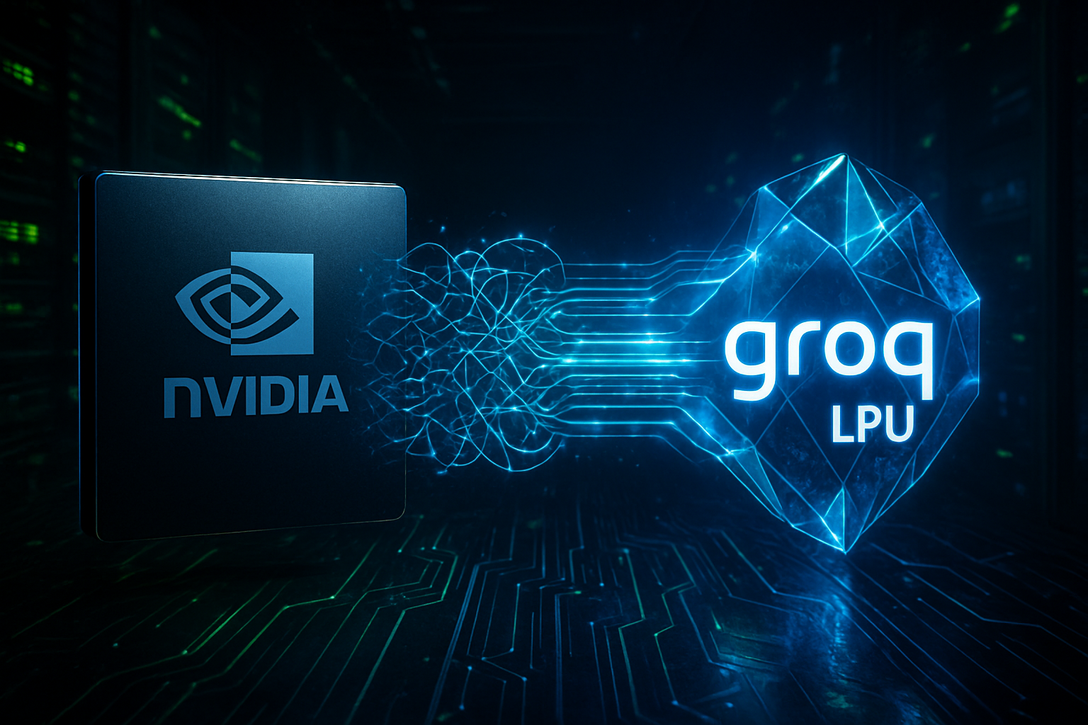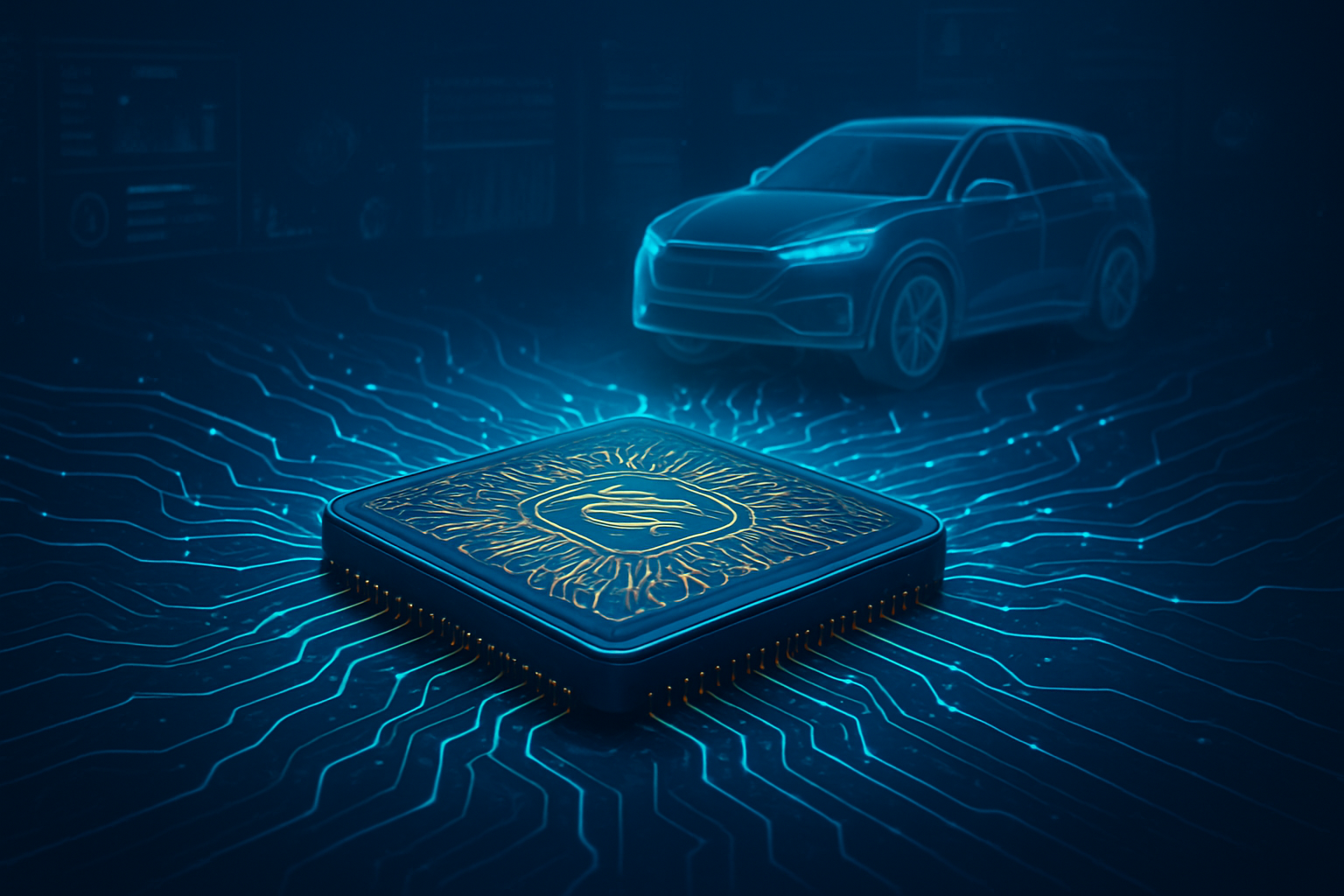
In a move that fundamentally redraws the competitive map of the automotive industry, Rivian (NASDAQ: RIVN) has officially unveiled its first custom-designed artificial intelligence processor, the Rivian Autonomy Processor 1 (RAP1). Announced during the company’s inaugural "Autonomy & AI Day" in late December 2025, the RAP1 chip represents a bold pivot toward full vertical integration. By moving away from off-the-shelf silicon provided by NVIDIA (NASDAQ: NVDA), Rivian is positioning itself as a primary architect of its own technological destiny, aiming to deliver Level 4 (L4) autonomous driving capabilities across its entire vehicle lineup.
The transition to custom silicon is more than just a hardware upgrade; it is the cornerstone of Rivian’s "Software-Defined Vehicle" (SDV) strategy. The RAP1 chip is designed to act as the central nervous system for the next generation of Rivian vehicles, including the highly anticipated R2 and R3 models. This shift allows the automaker to optimize its AI models directly for its hardware, promising a massive leap in compute efficiency and a significant reduction in power consumption—a critical factor for extending the range of electric vehicles. As the industry moves toward "Eyes-Off" autonomy, Rivian’s decision to build its own brain suggests that the era of general-purpose automotive chips may be nearing its twilight for the industry's top-tier players.
Technical Specifications and the L4 Vision
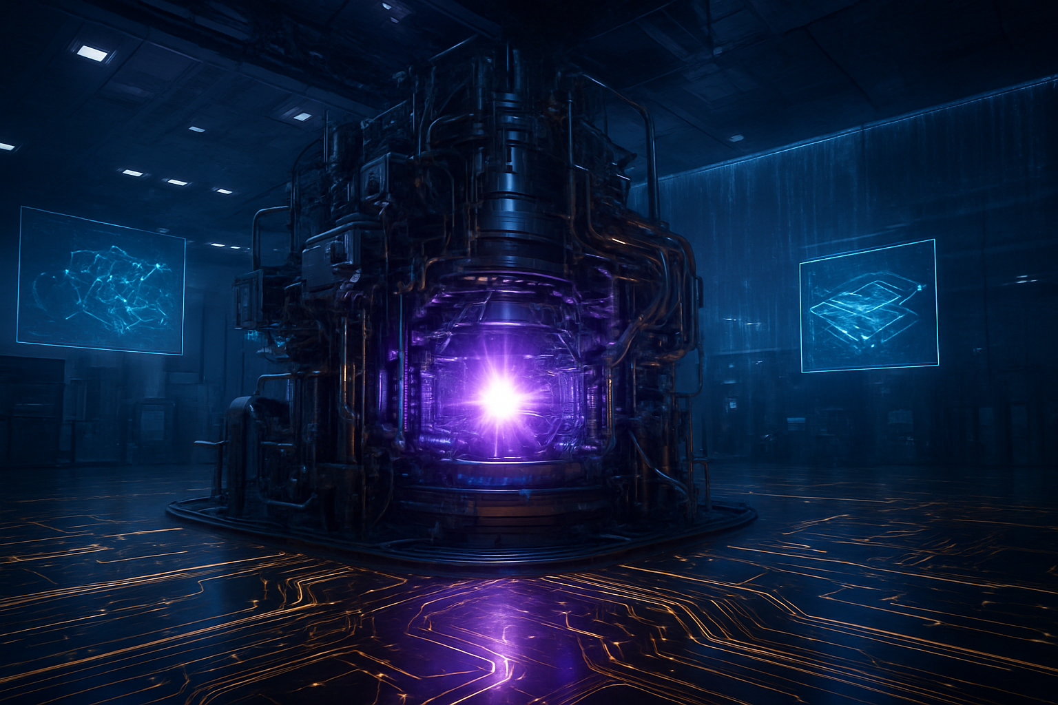
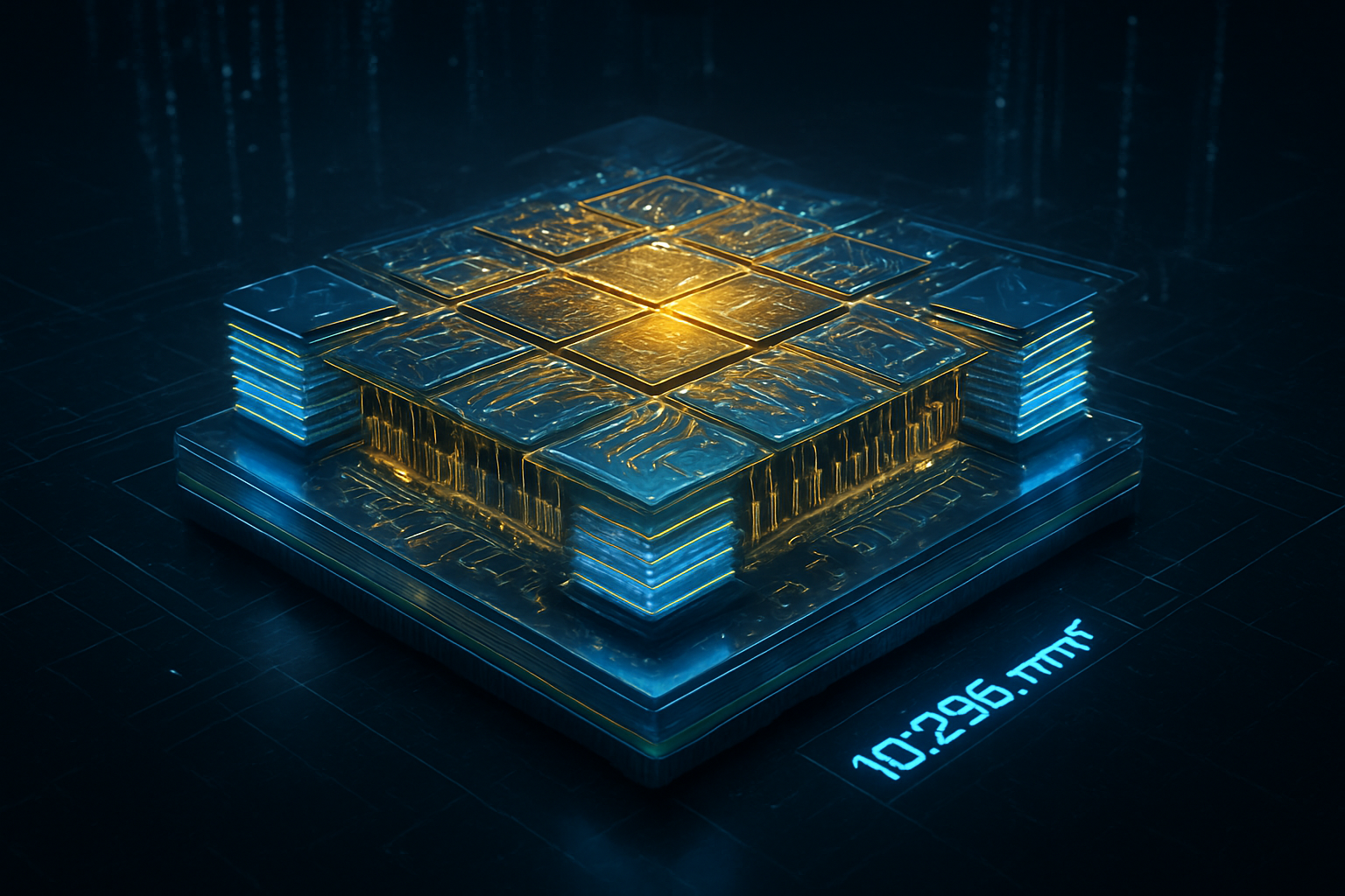
The RAP1 is a technical powerhouse, manufactured on a cutting-edge 5nm process by TSMC (NYSE: TSM). Built on the Armv9 architecture in close collaboration with Arm Holdings (NASDAQ: ARM), the chip is the first in the automotive sector to deploy the Arm Cortex-A720AE CPU cores. This "Automotive Enhanced" (AE) IP is specifically designed for high-performance computing in safety-critical environments. The RAP1 architecture features a Multi-Chip Module (MCM) design that integrates 14 high-performance application cores with 8 dedicated safety-island cores, ensuring that the vehicle can maintain operational integrity even in the event of a primary logic failure.
In terms of raw AI performance, the RAP1 delivers a staggering 800 TOPS (Trillion Operations Per Second) per chip. When deployed in Rivian’s new Autonomy Compute Module 3 (ACM3), a dual-RAP1 configuration provides 1,600 sparse INT8 TOPS—a fourfold increase over the NVIDIA DRIVE Orin systems previously utilized by the company. This massive compute overhead is necessary to process the 5 billion pixels per second flowing from Rivian’s suite of 11 cameras, five radars, and newly standardized LiDAR sensors. This multi-modal approach to sensor fusion stands in stark contrast to the vision-only strategy championed by Tesla (NASDAQ: TSLA), with Rivian betting that the RAP1’s ability to reconcile data from diverse sensors will be the key to achieving true L4 safety.
Initial reactions from the AI research community have been overwhelmingly positive, particularly regarding Rivian’s "Large Driving Model" (LDM). This foundational AI model is trained using Group-Relative Policy Optimization (GRPO), a technique similar to those used in advanced Large Language Models. By distilling this massive model to run natively on the RAP1’s neural engine, Rivian has created a system capable of complex reasoning in unpredictable urban environments. Industry experts have noted that the RAP1’s proprietary "RivLink" interconnect—a low-latency bridge between chips—allows for nearly linear scaling of performance, potentially future-proofing the hardware for even more advanced AI agents.
Disruption in the Silicon Ecosystem
The introduction of the RAP1 chip is a direct challenge to NVIDIA’s long-standing dominance in the automotive AI space. While NVIDIA remains a titan in data center AI, Rivian’s departure highlights a growing trend among "Tier 1" EV manufacturers to reclaim their hardware margins and development timelines. By eliminating the "vendor margin" paid to third-party silicon providers, Rivian expects to significantly improve its unit economics as it scales production of the R2 platform. Furthermore, owning the silicon allows Rivian’s software engineers to begin optimizing code for new hardware nearly a year before the chips are even fabricated, drastically accelerating the pace of innovation.
Beyond NVIDIA, this development has significant implications for the broader tech ecosystem. Arm Holdings stands to benefit immensely as its AE (Automotive Enhanced) architecture gains a flagship proof-of-concept in the RAP1. This partnership validates Arm’s strategy of moving beyond smartphones into high-performance, safety-critical compute. Meanwhile, the $5.8 billion joint venture between Rivian and Volkswagen (OTC: VWAGY) suggests that the RAP1 could eventually find its way into high-end European models from Porsche and Audi. This could effectively turn Rivian into a silicon and software supplier to legacy OEMs, creating a new high-margin revenue stream that rivals its vehicle sales.
However, the move also puts pressure on other EV startups and legacy manufacturers who lack the capital or expertise to design custom silicon. Companies like Lucid or Polestar may find themselves increasingly reliant on NVIDIA or Qualcomm, potentially falling behind in the race for specialized, power-efficient autonomy. The market positioning is clear: Rivian is no longer just an "adventure vehicle" company; it is a vertically integrated technology powerhouse competing directly with Tesla for the title of the most advanced software-defined vehicle platform in the world.
The Milestone of Vertical Integration
The broader significance of the RAP1 chip lies in the shift from "hardware-first" to "AI-first" vehicle architecture. In the past, cars were a collection of hundreds of independent Electronic Control Units (ECUs) from various suppliers. Rivian’s zonal architecture, powered by RAP1, collapses this complexity into a unified system. This is a milestone in the evolution of the Software-Defined Vehicle, where the hardware is a generic substrate and the value is almost entirely defined by the AI models running on top of it. This transition mirrors the evolution of the smartphone, where the integration of custom silicon (like Apple’s A-series chips) became the primary differentiator for user experience and performance.
There are, however, potential concerns regarding this level of vertical integration. As vehicles become increasingly reliant on a single, proprietary silicon platform, questions about long-term repairability and "right to repair" become more urgent. If a RAP1 chip fails ten years from now, owners will be entirely dependent on Rivian for a replacement, as there are no third-party equivalents. Furthermore, the concentration of so much critical functionality into a single compute module raises the stakes for cybersecurity. Rivian has addressed this by implementing hardware-level encryption and a "Safety Island" within the RAP1, but the centralized nature of SDVs remains a high-value target for sophisticated actors.
Comparatively, the RAP1 launch can be viewed as Rivian’s "M1 moment." Much like when Apple transitioned the Mac to its own silicon, Rivian is breaking free from the constraints of general-purpose hardware to unlock features that were previously impossible. This move signals that for the winners of the AI era, being a "customer" of AI hardware is no longer enough; one must be a "creator" of it. This shift reflects a maturing AI landscape where the most successful companies are those that can co-design their algorithms and their transistors in tandem.
Future Roadmaps and Challenges
Looking ahead, the near-term focus for Rivian will be the integration of RAP1 into the R2 and R3 production lines, slated for late 2026. These vehicles are expected to ship with the necessary hardware for L4 autonomy as standard, allowing Rivian to monetize its "Autonomy+" subscription service. Experts predict that the first "Eyes-Off" highway pilot programs will begin in select states by mid-2026, utilizing the RAP1’s massive compute headroom to handle edge cases that currently baffle Level 2 systems.
In the long term, the RAP1 architecture is expected to evolve into a family of chips. Rumors of a "RAP2" are already circulating in Silicon Valley, with speculation that it will focus on even higher levels of integration, potentially combining the infotainment and autonomy processors into a single "super-chip." The biggest challenge remaining is the regulatory landscape; while the hardware is ready for L4, the legal frameworks for liability in "Eyes-Off" scenarios are still being written. Rivian’s success will depend as much on its lobbying and safety record as it does on its 5nm transistors.
Summary and Final Assessment
The unveiling of the RAP1 chip is a watershed moment for Rivian and the automotive industry at large. By successfully designing and deploying custom AI silicon on the Arm platform, Rivian has proven that it can compete at the highest levels of semiconductor engineering. The move effectively ends the company’s reliance on NVIDIA, slashes power consumption, and provides the raw horsepower needed for the next decade of autonomous driving. It is a definitive statement that the future of the car is not just electric, but deeply intelligent and vertically integrated.
As we move through 2026, the industry will be watching closely to see how the RAP1 performs in real-world conditions. The key takeaways are clear: vertical integration is the new gold standard, custom silicon is the prerequisite for L4 autonomy, and the software-defined vehicle is finally arriving. For investors and consumers alike, the RAP1 isn't just a chip—it's the engine of Rivian’s second act.
This content is intended for informational purposes only and represents analysis of current AI developments.
TokenRing AI delivers enterprise-grade solutions for multi-agent AI workflow orchestration, AI-powered development tools, and seamless remote collaboration platforms.
For more information, visit https://www.tokenring.ai/.