As the artificial intelligence industry pivots toward the unprecedented scale of multi-trillion-parameter models, the bottleneck has shifted from raw compute to the networking fabric that binds tens of thousands of processors together. In a landmark announcement at the start of February 2026, NVIDIA (NASDAQ: NVDA) has officially detailed the full integration of Silicon Photonics into its Spectrum-X1600 Ethernet platform. Designed specifically for the upcoming Rubin-class GPU architecture, this development marks a transition from traditional electrical signaling to a predominantly optical data center fabric, promising to slash latency and power consumption at a moment when the industry faces a looming energy crisis.
The significance of this advancement cannot be overstated. By co-packaging optical engines directly with the switch silicon—a technology known as Co-Packaged Optics (CPO)—NVIDIA is effectively dismantling the "Power Wall" that has threatened to stall the growth of "AI Factories." For hyperscalers and enterprise giants, the Spectrum-X Ethernet Photonics platform provides the first viable blueprint for scaling clusters to over one million GPUs, ensuring that the physical limits of copper and electricity do not impede the next generation of generative AI breakthroughs.
Breaking the 1.6 Terabit Barrier with Silicon Photonics
The core of this announcement lies in the new Spectrum-X1600 platform (SN6000 series), which transitions the industry into the 1.6 Terabit (1.6T) era. Built upon the Spectrum-6 ASIC, the platform utilizes 224G SerDes technology to deliver a staggering 409.6 Tb/s of aggregate throughput in a single switch chassis. Unlike its predecessors, which relied on pluggable OSFP transceivers, the Spectrum-X1600 utilizes Silicon Photonics to integrate the optical conversion process directly onto the processor package. This shift eliminates the need for power-hungry Digital Signal Processors (DSPs) typically found in pluggable modules, resulting in a 5x reduction in power consumption per port. In a massive 400,000-GPU data center, this optimization alone can reduce total networking power requirements from 72 MW to just over 21 MW.
Technically, the integration of photonics directly into the switch and the ConnectX-9 SuperNIC minimizes the electrical signal path from several inches of PCB trace to a few millimeters. This drastic reduction in distance mitigates signal degradation and brings end-to-end latency down to a consistent 0.5 microseconds. For the "all-reduce" operations essential to Mixture of Experts (MoE) AI architectures, this low-jitter environment is critical. It prevents "tail latency" events where a single delayed packet can stall thousands of GPUs, effectively increasing the overall utilization efficiency of the Rubin clusters.
NVIDIA has also addressed the long-standing industry concern regarding the serviceability of Co-Packaged Optics. Historically, if an integrated optical engine failed, the entire switch ASIC would need to be replaced. To counter this, NVIDIA introduced a detachable "Scale-Up CPO" design, which allows individual optical engines to be swapped out without discarding the underlying silicon. This innovation has been met with early praise from the AI research community and infrastructure engineers, who see it as the "missing link" that makes CPO a viable standard for high-availability production environments.
Initial reactions from industry experts suggest that NVIDIA’s "full-stack" approach is widening its lead over traditional networking vendors. By tightly coupling the Rubin GPU, the Vera CPU, and the Spectrum-X1600 switch into a single, cohesive optical fabric, NVIDIA is creating a deterministic networking environment that mimics the performance of its proprietary InfiniBand protocol while maintaining the broad compatibility of Ethernet. This "best of both worlds" scenario is designed to capture the growing segment of the market that is moving away from closed systems toward standard Ethernet-based AI back-ends.
The Competitive Shift: Ethernet vs. InfiniBand and the Rise of UEC
The strategic move to dominate 1.6T Ethernet places NVIDIA in direct competition with merchant silicon heavyweights like Broadcom (NASDAQ: AVGO) and Marvell (NASDAQ: MRVL). Broadcom’s Tomahawk 6 and Marvell’s Teralynx 11 are also targeting the 1.6T milestone, but they rely heavily on the burgeoning Ultra Ethernet Consortium (UEC) standards to attract hyperscalers who are wary of NVIDIA’s ecosystem lock-in. While Broadcom offers a "disaggregated" approach where customers can pick and choose their optics, NVIDIA is betting that hyperscalers will pay a premium for a "black box" solution where the photonics, the switch, and the GPU are pre-optimized for one another.
For tech giants like Meta (NASDAQ: META), Microsoft (NASDAQ: MSFT), and Alphabet (NASDAQ: GOOGL), the Spectrum-X1600 presents a complex choice. Meta has already deployed Spectrum-X for its latest Llama 5 training clusters to achieve maximum performance, yet it remains a founding member of the UEC, seeking an "off-ramp" to lower-cost, open-source networking in the future. Microsoft, meanwhile, continues to balance its Azure-OpenAI partnership’s reliance on NVIDIA’s stack with its internal "Maia" accelerator and UEC-compliant networking projects. The integration of Silicon Photonics into the NVIDIA stack effectively raises the barrier to entry for these internal projects, as matching NVIDIA’s power efficiency requires mastering high-risk 3D-stacked optical manufacturing.
The market implications are substantial, with analysts from IDC and Gartner projecting the AI networking Total Addressable Market (TAM) to exceed $80 billion by 2027. Nearly 20% of all Ethernet switch ports sold globally are now expected to be dedicated to AI workloads. By commoditizing Silicon Photonics within its own hardware, NVIDIA is positioning itself not just as a chip maker, but as a dominant provider of the entire data center's nervous system. This vertical integration makes it increasingly difficult for specialized optics manufacturers or legacy networking firms like Cisco (NASDAQ: CSCO) to compete on the grounds of power efficiency and reliability alone.
Scaling Laws and the End of the Electrical Era
On a broader level, the move to Spectrum-X Ethernet Photonics signals a fundamental shift in the AI landscape: the end of the purely electrical era of computing. As AI models continue to scale according to "Scaling Laws," the energy required to move data between chips has become a larger hurdle than the energy required to perform the calculations. NVIDIA’s pivot to photonics is a recognition that without light-based communication, the roadmap to AGI (Artificial General Intelligence) would eventually be stopped by the sheer physics of heat and resistance in copper wiring.
This development also addresses growing global concerns over the environmental impact of AI. By reducing networking power by up to 70% in Rubin-class clusters, NVIDIA is providing a path forward for sustainability in the era of "Million-GPU" deployments. However, this transition is not without concerns. The concentration of such critical infrastructure technology within a single vendor raises questions about long-term industry resilience and the "proprietary tax" that could be levied on the future of AI development. Comparisons are already being drawn to the early days of the internet, where proprietary protocols eventually gave way to open standards, though NVIDIA's lead in CPO manufacturing may delay that cycle for years.
The Road Ahead: 3.2T and the 'Feynman' Architecture
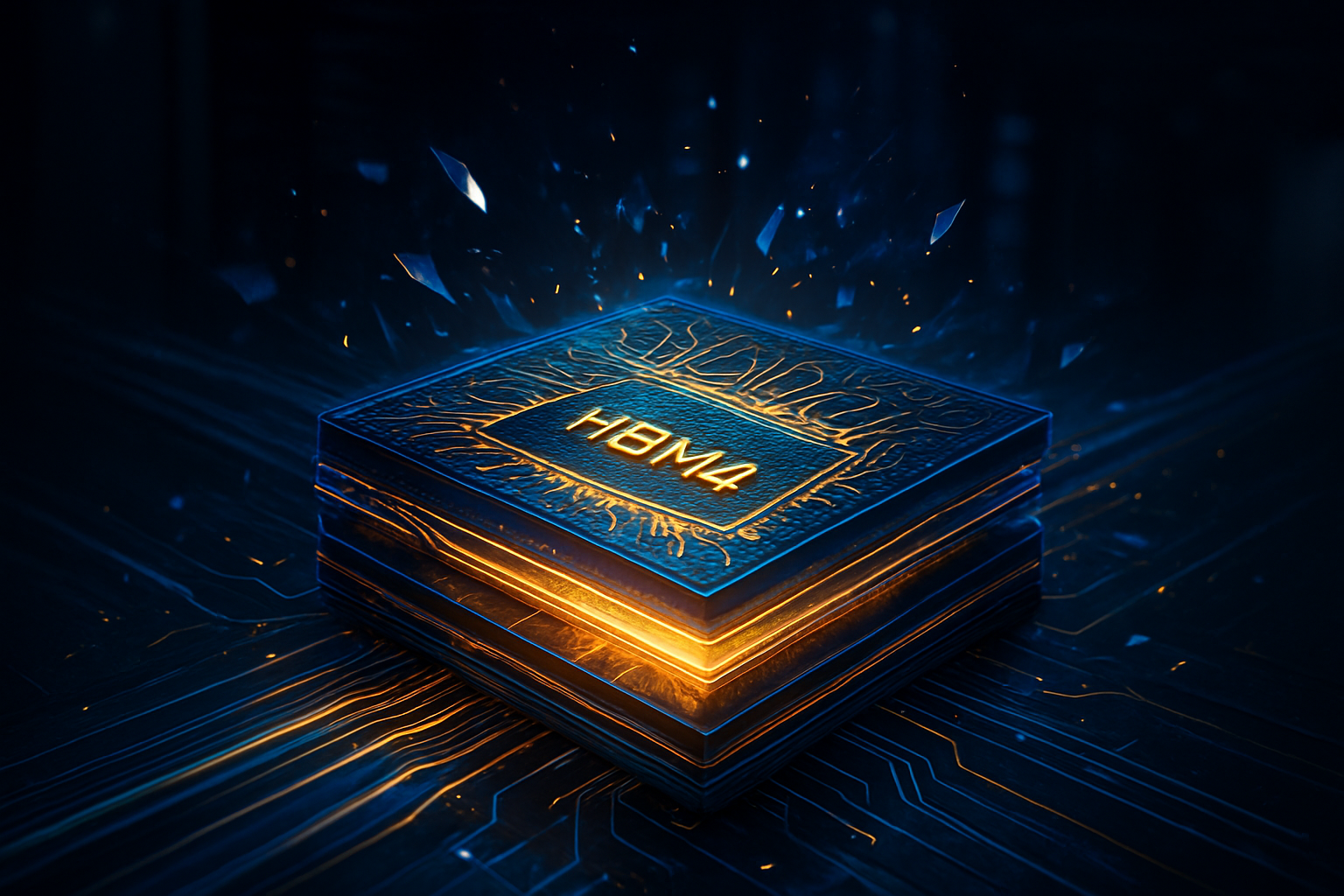
Looking toward the future, the Spectrum-X1600 is likely just the beginning of NVIDIA's optical journey. Near-term developments are expected to focus on the 3.2 Terabit (3.2T) era, which will likely require even more advanced modulation techniques such as PAM6 or PAM8 to overcome the signal integrity limits of current 448G SerDes. Experts predict that the successor to the Rubin architecture, codenamed "Feynman," will see Silicon Photonics moved even closer to the compute die, potentially utilizing 3D-stacked optical engines directly on top of the HBM4 memory stacks.
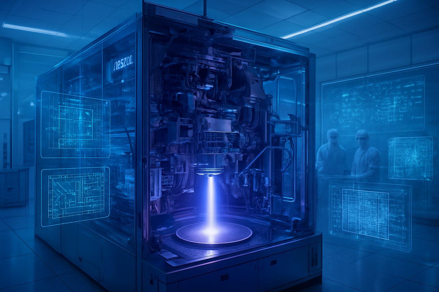
The next 18 to 24 months will be a period of intense validation for these CPO-enabled switches. While the technical specifications are impressive, the challenges of manufacturing high-yield photonics at TSMC’s 3nm and 2nm nodes remain significant. Furthermore, the industry must wait to see how the Ultra Ethernet Consortium responds. If the UEC can deliver a standardized CPO framework by late 2026, the competitive landscape could shift once again toward the disaggregated models favored by Google and Amazon (NASDAQ: AMZN).
A New Benchmark for AI Infrastructure
The announcement of NVIDIA Spectrum-X Ethernet Photonics for Rubin-class clusters marks a defining moment in the history of AI infrastructure. By successfully integrating Silicon Photonics into a scalable Ethernet platform, NVIDIA has provided the industry with the power and latency headroom necessary to reach for the next order of magnitude in model complexity. This is no longer just about faster chips; it is about a new architecture for the data center itself.
As we move through 2026, the key metrics to watch will be the real-world power savings reported by early Rubin adopters and the speed at which competitors can bring their own CPO solutions to market. If NVIDIA’s detachable CPO design proves as reliable as claimed, it may set the standard for high-performance networking for the remainder of the decade, cementing NVIDIA’s role as the indispensable architect of the AI era.
This content is intended for informational purposes only and represents analysis of current AI developments.
TokenRing AI delivers enterprise-grade solutions for multi-agent AI workflow orchestration, AI-powered development tools, and seamless remote collaboration platforms.
For more information, visit https://www.tokenring.ai/.