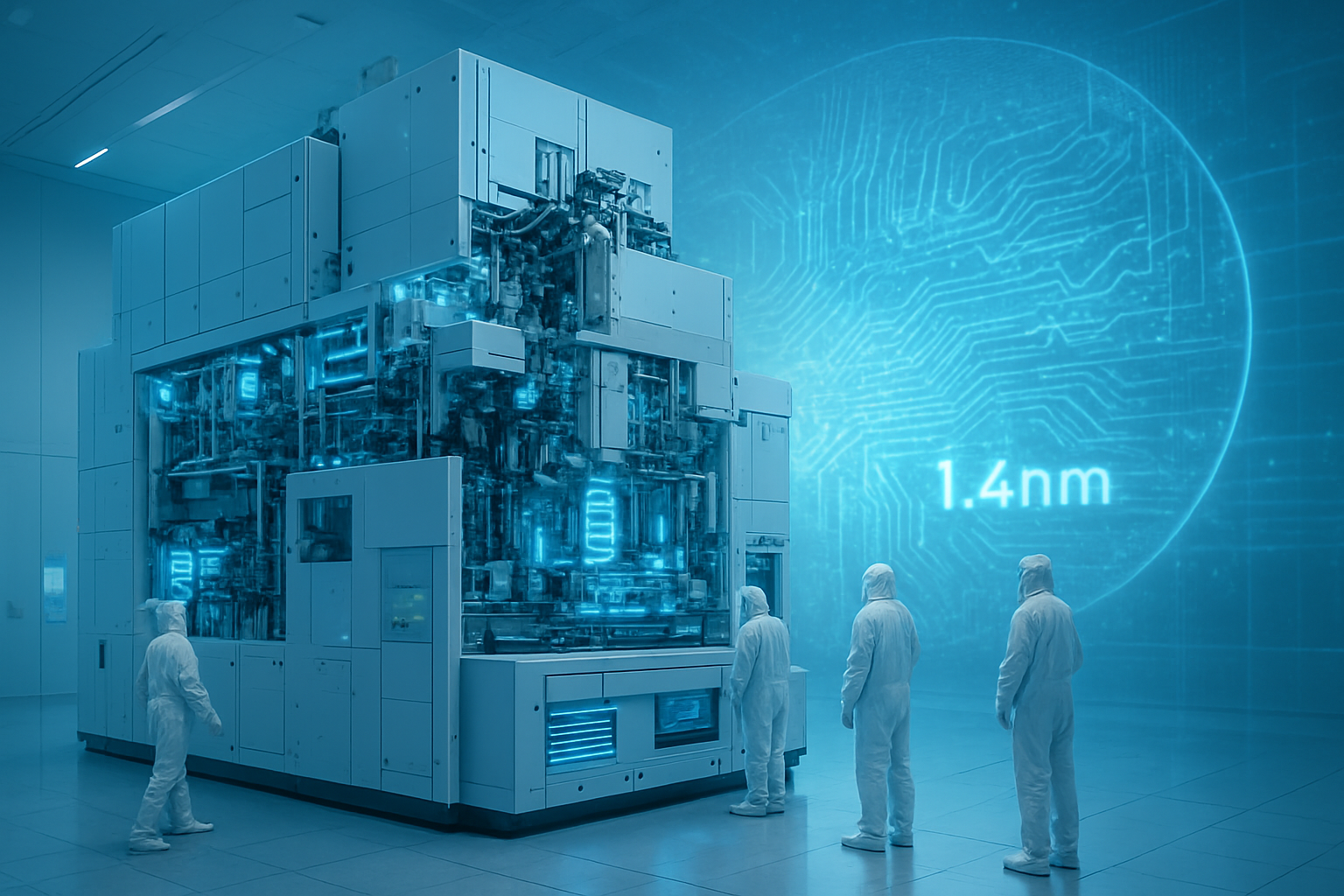
As of December 30, 2025, the narrative of the global AI race has shifted from a battle over transistor counts to a desperate scramble for "back-end" real estate. For the past decade, the semiconductor industry focused on the front-end—the complex lithography required to etch circuits onto silicon wafers. However, in the closing days of 2025, the industry has hit a physical wall. The primary bottleneck for the world’s most powerful AI chips is no longer the ability to print them, but the ability to package them. Advanced packaging technologies like TSMC’s CoWoS and Intel’s Foveros have become the most precious commodities in the tech world, dictating the pace of progress for every major AI lab from San Francisco to Beijing.
The significance of this shift cannot be overstated. With lead times for flagship AI accelerators like NVIDIA’s Blackwell architecture stretching to 18 months, the "Silicon Squeeze" has turned advanced packaging into a strategic geopolitical asset. As demand for generative AI and massive language models continues to outpace supply, the ability to "stitch" together multiple silicon dies into a single high-performance module is the only way to bypass the physical limits of traditional chip manufacturing. In 2025, the "chiplet" revolution has officially arrived, and those who control the packaging lines now control the future of artificial intelligence.
The Technical Wall: Reticle Limits and the Rise of CoWoS-L
The technical crisis of 2025 stems from a physical constraint known as the "reticle limit." For years, semiconductor manufacturers like Taiwan Semiconductor Manufacturing Co. (NYSE: TSM) could simply make a single chip larger to increase its power. However, standard lithography tools can only expose an area of approximately 858 mm² at once. NVIDIA (NASDAQ: NVDA) reached this limit with its previous generations, but the demands of 2025-era AI require far more silicon than a single exposure can provide. To solve this, the industry has moved toward heterogeneous integration—combining multiple smaller "chiplets" onto a single substrate to act as one giant processor.
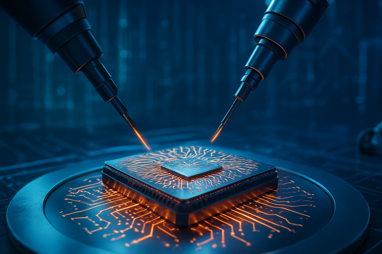
TSMC has maintained its lead through CoWoS-L (Chip on Wafer on Substrate – Local Silicon Interconnect). Unlike previous iterations that used a massive, expensive silicon interposer, CoWoS-L utilizes tiny silicon bridges to link dies with massive bandwidth. This technology is the backbone of the NVIDIA Blackwell (B200) and the upcoming Rubin (R100) architectures. The Rubin chip, entering volume production as 2025 draws to a close, is a marvel of engineering that scales to a "4x reticle" design, effectively stitching together four standard-sized chips into a single super-processor. This complexity, however, comes at a cost: yield rates for these multi-die modules remain volatile, and a single defect in one of the 16 integrated HBM4 (High Bandwidth Memory) stacks can ruin a module worth tens of thousands of dollars.
The High-Stakes Rivalry: Intel’s $5 Billion Diversification and AMD’s Acceleration
The packaging bottleneck has forced a radical reshuffling of industry alliances. In one of the most significant strategic pivots of the year, NVIDIA reportedly invested $5 billion into Intel (NASDAQ: INTC) Foundry Services in late 2025. This move was designed to secure capacity for Intel’s Foveros 3D stacking and EMIB (Embedded Multi-die Interconnect Bridge) technologies, providing NVIDIA with a vital "Plan B" to reduce its total reliance on TSMC. Intel’s aggressive expansion of its packaging facilities in Malaysia and Oregon has positioned it as the only viable Western alternative for high-end AI assembly, a goal CEO Pat Gelsinger has pursued relentlessly to revitalize the company’s foundry business.
Meanwhile, Advanced Micro Devices (NASDAQ: AMD) has accelerated its own roadmap to capitalize on the supply gaps. The AMD Instinct MI350 series, launched in mid-2025, utilizes a sophisticated 3D chiplet architecture that rivals NVIDIA’s Blackwell in memory density. To bypass the TSMC logjam, AMD has turned to "Outsourced Semiconductor Assembly and Test" (OSAT) giants like ASE Technology Holding (NYSE: ASX) and Amkor Technology (NASDAQ: AMKR). These firms are rapidly building out "CoWoS-like" capacity in Arizona and Taiwan, though they too are hampered by 12-month lead times for the specialized equipment required to handle the ultra-fine interconnects of 2025-grade silicon.
The Wider Significance: Geopolitics and the End of Monolithic Computing
The shift to advanced packaging represents the end of the "monolithic era" of computing. For fifty years, the industry followed Moore’s Law by shrinking transistors on a single piece of silicon. In 2025, that era is over. The future is modular, and the economic implications are profound. Because advanced packaging is so capital-intensive and requires such high precision, it has created a new "moat" that favors the largest incumbents. Hyperscalers like Meta (NASDAQ: META), Microsoft (NASDAQ: MSFT), and Amazon (NASDAQ: AMZN) are now pre-booking packaging capacity up to two years in advance, a practice that effectively crowds out smaller AI startups and academic researchers.
This bottleneck also has a massive impact on the global supply chain's resilience. Most advanced packaging still occurs in East Asia, creating a single point of failure that keeps policymakers in Washington and Brussels awake at night. While the U.S. CHIPS Act has funded domestic fabrication plants, the "back-end" packaging remains the missing link. In late 2025, we are seeing the first real efforts to "reshore" this capability, with new facilities in the American Southwest beginning to come online. However, the transition is slow; the expertise required for 2.5D and 3D integration is highly specialized, and the labor market for packaging engineers is currently the tightest in the tech sector.
The Next Frontier: Glass Substrates and Panel-Level Packaging
Looking toward 2026 and 2027, the industry is already searching for the next breakthrough to break the current bottleneck. The most promising development is the transition to glass substrates. Traditional organic substrates are prone to warping and heat-related issues as chips get larger and hotter. Glass offers superior flatness and thermal stability, allowing for even denser interconnects. Intel is currently leading the charge in glass substrate research, with plans to integrate the technology into its 2026 product lines. If successful, glass could allow for "system-in-package" designs that are significantly larger than anything possible today.
Furthermore, the industry is eyeing Panel-Level Packaging (PLP). Currently, chips are packaged on circular 300mm wafers, which results in significant wasted space at the edges. PLP uses large rectangular panels—similar to those used in the display industry—to process hundreds of chips at once. This could potentially increase throughput by 3x to 4x, finally easing the supply constraints that have defined 2025. However, the transition to PLP requires an entirely new ecosystem of equipment and materials, meaning it is unlikely to provide relief for the current Blackwell and MI350 backlogs until at least late 2026.
Summary of the 2025 Silicon Landscape
As 2025 draws to a close, the semiconductor industry has successfully navigated the challenges of sub-3nm fabrication, only to find itself trapped by the physical limits of how those chips are put together. The "Silicon Squeeze" has made advanced packaging the ultimate arbiter of AI power. NVIDIA’s 18-month lead times and the strategic move toward Intel’s packaging lines underscore a new reality: in the AI era, it’s not just about what you can build on the silicon, but how much silicon you can link together.
The coming months will be defined by how quickly TSMC, Intel, and Samsung (KRX: 005930) can scale their 3D stacking capacities. For investors and tech leaders, the metrics to watch are no longer just wafer starts, but "packaging out-turns" and "interposer yields." As we head into 2026, the companies that master the art of the chiplet will be the ones that define the next plateau of artificial intelligence. The revolution is no longer just in the code—it’s in the package.
This content is intended for informational purposes only and represents analysis of current AI developments.
TokenRing AI delivers enterprise-grade solutions for multi-agent AI workflow orchestration, AI-powered development tools, and seamless remote collaboration platforms.
For more information, visit https://www.tokenring.ai/.