As of December 19, 2025, the artificial intelligence landscape has undergone a fundamental transformation. The era of "General AI" hype—characterized by the initial explosion of large language models (LLMs)—has matured into the era of "Vertical AI." Investors are no longer captivated by simple chatbots; instead, the market is rewarding companies that have built deep, industry-specific moats and edge-computing capabilities. This shift has placed three distinct players—SoundHound AI, BigBear.ai, and Tempus AI—at the center of the financial conversation as we head into 2026.
While the broader tech indices have faced volatility due to shifting interest rates and a retrenchment from peak 2024 valuations, these three firms have demonstrated that the real value of AI lies in its application to physical and specialized digital workflows. From voice-enabled commerce in our vehicles to autonomous threat detection on the battlefield and precision oncology in the clinic, the "Intelligence Revolution" has moved from the cloud to the edge, fundamentally changing how enterprises and governments operate.
The Technical Edge: Polaris, ConductorOS, and the Data Moat
The technical narrative of late 2025 is dominated by specialized model architectures. SoundHound AI (NASDAQ:SOUN) has solidified its position with the launch of its Polaris foundation model. Unlike general-purpose models, Polaris is engineered specifically for "Voice Commerce" and agentic workflows. It boasts a 40% improvement in accuracy over its 2024 predecessors, specifically in high-noise environments like restaurant drive-thrus and moving vehicles. This is achieved through a proprietary "Dynamic Interaction" engine that processes speech and intent simultaneously, rather than sequentially, reducing latency to near-human levels.
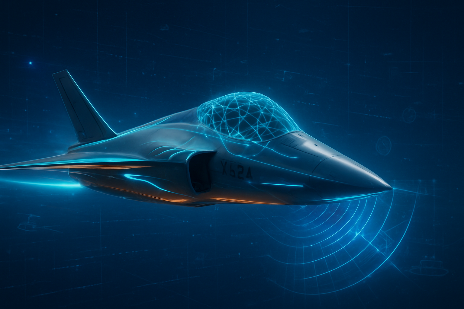
In the defense sector, BigBear.ai (NYSE:BBAI) has pivoted toward "Edge Sensor Fusion" with its ConductorOS platform. In a landmark partnership with C Speed in December 2025, BigBear.ai successfully integrated its AI into LightWave Radar systems. This allows for real-time, autonomous threat detection at the "sensor level," meaning the AI can identify and categorize adversarial threats without needing to send data back to a central server. This move into Edge AI addresses the critical bandwidth and latency constraints of modern electronic warfare, differentiating BigBear from competitors who remain tethered to cloud-heavy infrastructures.
Tempus AI (NASDAQ:TEM) has built what experts call the most significant "biological data moat" in history. By late 2025, the company has integrated clinical records and genomic data for over 45 million patients. Their latest technical milestone, the FDA 510(k) cleared Tempus Pixel device, uses digital pathology and AI to identify biomarkers that were previously invisible to the human eye. Furthermore, their generative AI clinical co-pilot, "David," is now integrated directly into major Electronic Health Record (EHR) systems, allowing doctors to query complex patient histories using natural language to find personalized treatment paths.
Market Positioning and the Competitive Landscape
The success of these companies has sent ripples through the tech industry, forcing giants like Microsoft (NASDAQ:MSFT) and Alphabet (NASDAQ:GOOGL) to reconsider their "one-size-fits-all" AI strategies. SoundHound’s aggressive M&A strategy—including the high-profile acquisitions of Amelia and Interactions—has allowed it to leapfrog traditional SaaS providers in the customer service and healthcare sectors. By controlling the entire voice stack, SoundHound has created a strategic advantage that is difficult for Big Tech to replicate without specialized hardware and automotive partnerships.
BigBear.ai’s focus on national security has carved out a niche that is increasingly insulated from the commercial AI "price wars." As the Department of Defense (DoD) prioritizes "Mission-Ready AI," BigBear’s $380 million backlog and its Virtual Anticipation Network (VANE) have made it a critical partner in geopolitical strategy. This positioning has forced traditional defense contractors to either partner with or look to acquire smaller, more agile AI firms to maintain their competitive edge in autonomous systems.
Tempus AI’s move into digital pathology through its acquisition of Paige has effectively cornered the market on "Intelligent Diagnostics." While pharmaceutical companies are spending billions on drug discovery, they are increasingly reliant on Tempus’s data library to identify the right patient cohorts for clinical trials. This has created a symbiotic relationship where Tempus acts as the "operating system" for precision medicine, a position that provides high-margin recurring revenue and a significant barrier to entry for new startups.
The Broader Significance: From Chatbots to Autonomous Agents
The market trends of late 2025 reflect a broader societal shift: the transition from AI as a tool to AI as an agent. We are no longer just asking AI questions; we are delegating tasks to it. SoundHound’s ability to facilitate hands-free commerce from a vehicle, BigBear’s autonomous threat detection, and Tempus’s automated clinical trial matching all represent the rise of "Agentic AI." These systems can plan, reason, and execute entire workflows with minimal human oversight, marking a milestone in the evolution of automation.
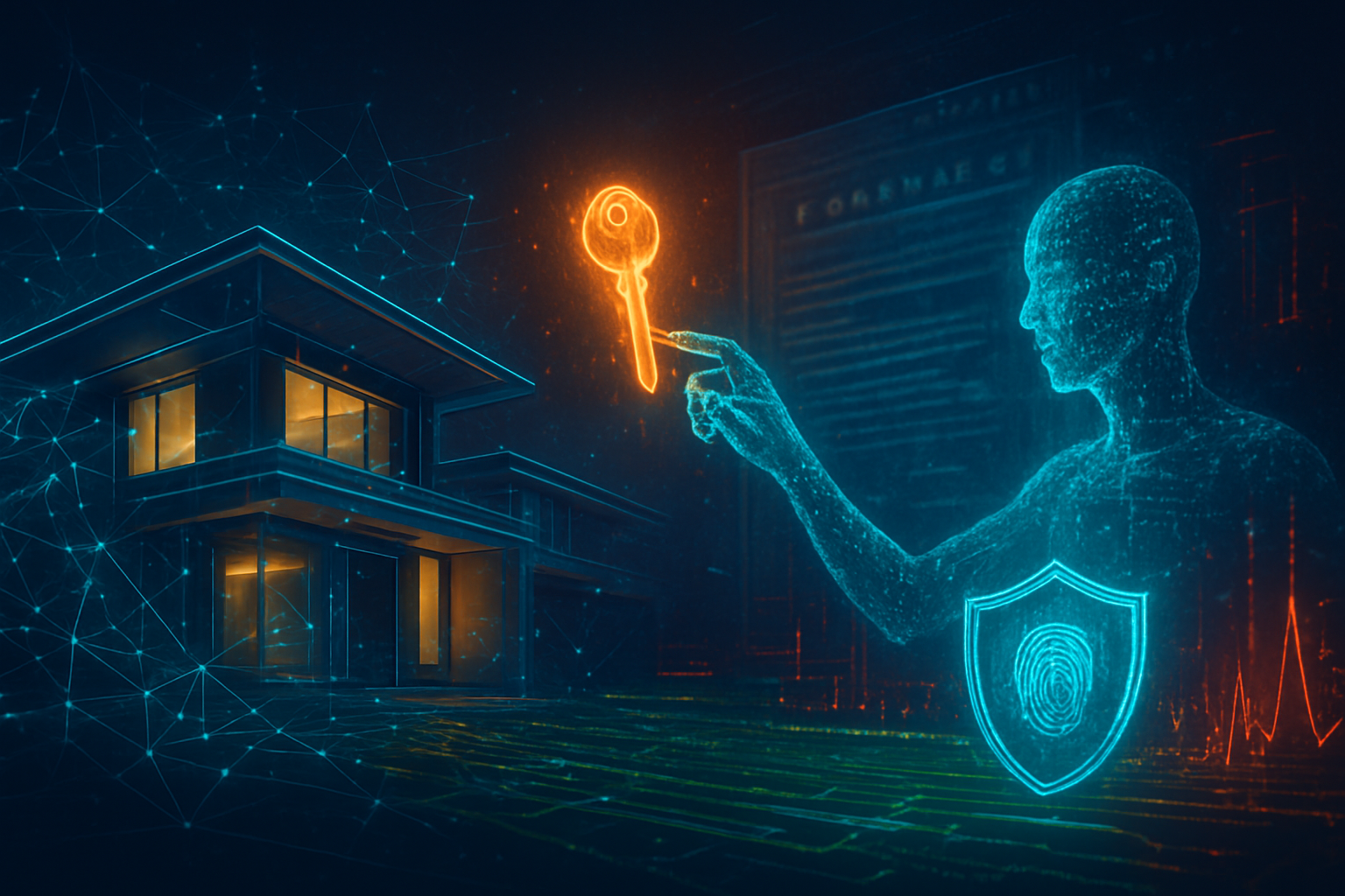
However, this rapid advancement has not come without concerns. The shift toward Edge AI—where data is processed locally on devices—is a direct response to the "privacy crisis" of 2024. By keeping sensitive medical, personal, and military data off the cloud, these companies are addressing one of the biggest hurdles to AI adoption. Yet, the "black box" nature of these specialized models continues to draw scrutiny from regulators, particularly in healthcare and defense, where the stakes of an AI error are life and death.
Compared to the "AI Summer" of 2023-2024, the current landscape is more pragmatic. The focus has shifted from "training-based compute" (building bigger models) to "inference-based compute" (running models efficiently). This shift favors companies like SoundHound and BigBear that have optimized their software to run on specialized, low-power semiconductors at the edge, rather than relying solely on massive Nvidia (NASDAQ:NVDA) H100 clusters.
Future Outlook: What to Expect in 2026
Looking ahead to 2026, experts predict that the "Vertical AI" trend will only accelerate. For SoundHound, the next frontier is the full integration of voice-AI into the "Smart Home" and "Smart City" infrastructure, moving beyond cars and restaurants. The company’s path to consistent profitability seems clear as they reach their goal of adjusted EBITDA positivity in the coming months, driven by their record $165M–$180M revenue guidance.
BigBear.ai is expected to expand its Malaysian and Middle Eastern aerospace hubs, potentially opening up new commercial revenue streams in logistics and supply chain management. The challenge for BigBear will be navigating the accounting and regulatory scrutiny that often follows rapid growth in government contracting. Meanwhile, Tempus AI is poised to become the first "AI-First" healthcare giant, with its revenue projected to exceed $1.26 billion as genomics testing becomes a standard of care globally.
The primary hurdle for all three companies remains the "talent war" and the cost of maintaining cutting-edge research. As AI models become more efficient, the differentiation will come from proprietary data access. Companies that own the data—like Tempus in healthcare or SoundHound in voice-commerce—will likely be the long-term winners in an increasingly crowded field.
Final Assessment: The New AI Guard
In summary, SoundHound AI, BigBear.ai, and Tempus AI represent the "New Guard" of the AI sector. They have successfully navigated the transition from the experimental phase of generative AI to the implementation phase of vertical, agentic solutions. Their performance in late 2025 serves as a blueprint for how AI companies can build sustainable businesses by solving specific, high-value problems rather than chasing general-purpose benchmarks.
As we move into 2026, the key indicators to watch will be the continued expansion of Edge AI capabilities and the successful integration of autonomous agents into everyday life. While the stock prices of these companies may remain volatile as the market adjusts to new valuation models, their technological impact is undeniable. They are no longer just "AI stocks"; they are the foundational players in the next era of the global economy.
This content is intended for informational purposes only and represents analysis of current AI developments.
TokenRing AI delivers enterprise-grade solutions for multi-agent AI workflow orchestration, AI-powered development tools, and seamless remote collaboration platforms.
For more information, visit https://www.tokenring.ai/.