Author: mdierolf

  • The Great Silicon Pivot: RISC-V Shatters the Data Center Duopoly as AI Demands Customization

    The Great Silicon Pivot: RISC-V Shatters the Data Center Duopoly as AI Demands Customization

    The landscape of data center architecture has reached a historic turning point. In a move that signals the definitive end of the decades-long x86 and ARM duopoly, Qualcomm (NASDAQ: QCOM) announced this week its acquisition of Ventana Micro Systems, the leading developer of high-performance RISC-V server CPUs. This acquisition, valued at approximately $2.4 billion, represents the largest validation to date of the open-source RISC-V instruction set architecture (ISA) as a primary contender for the future of artificial intelligence and cloud infrastructure.

    The significance of this shift cannot be overstated. As the "Transformer era" of AI places unprecedented demands on power efficiency and memory bandwidth, the rigid licensing models and fixed instruction sets of traditional chipmakers are being bypassed in favor of "silicon sovereignty." By leveraging RISC-V, hyperscalers and chip designers are now able to build domain-specific hardware—tailoring silicon at the gate level to optimize for the specific matrix math and vector processing required by large language models (LLMs).

    The Technical Edge: RVA23 and the Rise of "Custom-Fit" Silicon

    The technical breakthrough propelling RISC-V into the data center is the recent ratification of the RVA23 profile. Previously, RISC-V faced criticism for "fragmentation"—the risk that software written for one RISC-V chip wouldn't run on another. The RVA23 standard, finalized in late 2024, mandates critical features like Hypervisor and Vector extensions, ensuring that standard Linux distributions can run seamlessly across diverse hardware. This standardization, combined with the launch of Ventana’s Veyron V2 platform and Tenstorrent’s Blackhole architecture, has provided the performance parity needed to challenge high-end Xeon and EPYC processors.

    Tenstorrent, led by legendary architect Jim Keller, recently began volume shipments of its Blackhole developer kits. Unlike traditional CPUs that treat AI as an offloaded task, Blackhole integrates RISC-V cores directly with "Tensix" matrix math units on a 6nm process. This architecture offers roughly 2.6 times the performance of its predecessor, Wormhole, by utilizing a 400 Gbps Ethernet-based "on-chip" network that allows thousands of chips to act as a single, unified AI processor. The technical advantage here is "hardware-software co-design": designers can add custom instructions for specific AI kernels, such as sparse tensor operations, which are difficult to implement on the more restrictive ARM (NASDAQ: ARM) or x86 architectures.

    Initial reactions from the research community have been overwhelmingly positive, particularly regarding the flexibility of the RISC-V Vector (RVV) 1.0 extension. Experts note that while ARM's Scalable Vector Extension (SVE) is powerful, RISC-V allows for variable vector lengths that better accommodate the sparse data sets common in modern recommendation engines and generative AI. This level of granularity allows for a 40% to 50% improvement in energy efficiency for inference tasks—a critical metric as data center power consumption becomes a global bottleneck.

    Hyperscale Integration and the Competitive Fallout

    The acquisition of Ventana by Qualcomm is part of a broader trend of vertical integration among tech giants. Meta (NASDAQ: META) has already begun deploying its MTIA 2i (Meta Training and Inference Accelerator) at scale, which utilizes RISC-V cores to handle complex recommendation workloads. In October 2025, Meta further solidified its position by acquiring Rivos, a startup specializing in CUDA-compatible RISC-V designs. This move is a direct shot across the bow of Nvidia (NASDAQ: NVDA), as it aims to bridge the software gap that has long kept developers locked into Nvidia's proprietary ecosystem.

    For incumbents like Intel (NASDAQ: INTC) and AMD (NASDAQ: AMD), the rise of RISC-V represents a fundamental threat to their data center margins. While Intel has joined the RISE (RISC-V Software Ecosystem) project to hedge its bets, the open-source nature of RISC-V allows customers like Google (NASDAQ: GOOGL) and Amazon (NASDAQ: AMZN) to design their own "host" CPUs for their AI accelerators without paying the "x86 tax" or being subject to ARM’s increasingly complex licensing fees. Google has already confirmed it is porting its internal software stack—comprising over 30,000 applications—to RISC-V using AI-powered migration tools.

    The competitive landscape is also shifting toward "sovereign compute." In Europe, the Quintauris consortium—a joint venture between Bosch, Infineon, Nordic, NXP, and Qualcomm—is aggressively funding RISC-V development to reduce the continent's reliance on US-controlled proprietary architectures. This suggests a future where the data center market is no longer dominated by a few central vendors, but rather by a fragmented yet interoperable ecosystem of specialized silicon.

    Geopolitics and the "Linux of Hardware" Moment

    The rise of RISC-V is inextricably linked to the current geopolitical climate. As US export controls continue to restrict the flow of high-end AI chips to China, the open-source nature of RISC-V has provided a lifeline for Chinese tech giants. Alibaba’s (NYSE: BABA) T-Head division recently unveiled the XuanTie C930, a server-grade processor designed to be entirely independent of Western proprietary ISAs. This has turned RISC-V into a "neutral" ground for global innovation, managed by the RISC-V International organization in Switzerland.

    This "neutrality" has led many industry analysts to compare the current moment to the rise of Linux in the 1990s. Just as Linux broke the monopoly of proprietary operating systems by providing a shared, communal foundation, RISC-V is doing the same for hardware. By commoditizing the instruction set, the industry is shifting its focus from "who owns the ISA" to "who can build the best implementation." This democratization of chip design allows startups to compete on merit rather than on the size of their patent portfolios.

    However, this transition is not without concerns. The failure of Esperanto Technologies earlier this year serves as a cautionary tale; despite having a highly efficient 1,000-core RISC-V chip, the company struggled to adapt its architecture to the rapidly evolving "transformer" models that now dominate AI. This highlights the risk of "over-specialization" in a field where the state-of-the-art changes every few months. Furthermore, while the RVA23 profile solves many compatibility issues, the "software moat" built by Nvidia’s CUDA remains a formidable barrier for RISC-V in the high-end training market.

    The Horizon: From Inference to Massive-Scale Training

    In the near term, expect to see RISC-V dominate the AI inference market, particularly for "edge-cloud" applications where power efficiency is paramount. The next major milestone will be the integration of RISC-V into massive-scale AI training clusters. Tenstorrent’s upcoming "Grendel" chip, expected in late 2026, aims to challenge Nvidia's Blackwell successor by utilizing a completely open-source software stack from the compiler down to the firmware.

    The primary challenge remaining is the maturity of the software ecosystem. While projects like RISE are making rapid progress in optimizing compilers like LLVM and GCC for RISC-V, the library support for specialized AI frameworks still lags behind x86. Experts predict that the next 18 months will see a surge in "AI-for-AI" development—using machine learning to automatically optimize RISC-V code, effectively closing the performance gap that previously took decades to bridge via manual tuning.

    A New Era of Compute

    The events of late 2025 have confirmed that RISC-V is no longer a niche curiosity; it is the new standard for the AI era. The Qualcomm-Ventana deal and the mass deployment of RISC-V silicon by Meta and Google signal a move away from "one-size-fits-all" computing toward a future of hyper-optimized, open-source hardware. This shift promises to lower the cost of AI compute, accelerate the pace of innovation, and redistribute the balance of power in the semiconductor industry.

    As we look toward 2026, the industry will be watching the performance of Tenstorrent’s Blackhole clusters and the first fruits of Qualcomm’s integrated RISC-V server designs. The "Great Silicon Pivot" is well underway, and for the first time in the history of the data center, the blueprints for the future are open for everyone to read, modify, and build upon.


    This content is intended for informational purposes only and represents analysis of current AI developments.

    TokenRing AI delivers enterprise-grade solutions for multi-agent AI workflow orchestration, AI-powered development tools, and seamless remote collaboration platforms.
    For more information, visit https://www.tokenring.ai/.

  • The Goldilocks Rally: How Cooling Inflation and the ‘Sovereign AI’ Boom Pushed Semiconductors to All-Time Highs

    The Goldilocks Rally: How Cooling Inflation and the ‘Sovereign AI’ Boom Pushed Semiconductors to All-Time Highs

    As 2025 draws to a close, the global financial markets are witnessing a historic convergence of macroeconomic stability and relentless technological expansion. On December 18, 2025, the semiconductor sector solidified its position as the undisputed engine of the global economy, with the PHLX Semiconductor Sector (SOX) Index hovering near its recent all-time high of 7,490.28. This massive rally, which has seen chip stocks surge by over 35% year-to-date, is being fueled by a "perfect storm": a decisive cooling of inflation that has allowed the Federal Reserve to pivot toward aggressive interest rate cuts, and a second wave of artificial intelligence (AI) investment known as "Sovereign AI."

    The significance of this moment cannot be overstated. For the past two years, the tech sector has grappled with the dual pressures of high borrowing costs and "AI skepticism." However, the November Consumer Price Index (CPI) report, which showed inflation dropping to a surprising 2.7%—well below the 3.1% forecast—has effectively silenced the bears. With the Federal Open Market Committee (FOMC) delivering its third consecutive 25-basis-point rate cut on December 10, the cost of capital for massive AI infrastructure projects has plummeted just as the industry transitions from the "training phase" to the even more compute-intensive "inference phase."

    The Rise of the 'Rubin' Era and the 3nm Transition

    The technical backbone of this rally lies in the rapid acceleration of the semiconductor roadmap, specifically the transition to 3nm process nodes and the introduction of next-generation architectures. NVIDIA (NASDAQ: NVDA) has dominated headlines with the formal preview of its "Vera Rubin" architecture, the successor to the highly successful Blackwell platform. Built on TSMC (NYSE: TSM) N3P (3nm) process, the Vera Rubin R100 GPU represents a paradigm shift from individual accelerators to "AI Factories." By utilizing advanced CoWoS-L packaging, NVIDIA has achieved a 4x reticle design, allowing for a staggering 50 PFLOPS of FP4 precision—roughly 2.5 times the performance of the Blackwell B200.

    While NVIDIA remains the leader, AMD (NASDAQ: AMD) has successfully carved out a massive share of the AI inference market with its Instinct MI350 series. Launched in late 2025, the MI350 is built on the CDNA 4 architecture and features 288GB of HBM3e memory. AMD’s strategic integration of ZT Systems has allowed the company to offer full-stack AI rack solutions that compete directly with NVIDIA’s GB200 NVL72 systems. Industry experts note that the MI350’s 35x improvement in inference efficiency over the previous generation has made it the preferred choice for hyperscalers like Meta (NASDAQ: META) and Microsoft (NASDAQ: MSFT), who are increasingly focused on the operational costs of running live AI models.

    The "bottleneck breaker" of late 2025, however, is High Bandwidth Memory 4 (HBM4). As GPU logic speeds have outpaced data delivery, the "Memory Wall" became a critical concern for AI developers. The shift to HBM4, led by SK Hynix (KRX: 000660) and Micron (NASDAQ: MU), has doubled the interface width to 2048-bit, providing up to 13.5 TB/s of bandwidth. This breakthrough allows a single GPU to hold trillion-parameter models in local memory, drastically reducing the latency and energy consumption associated with data transfer. Micron’s blowout earnings report on December 17, which sent the stock up 15%, served as a validation of this trend, proving that the AI rally is no longer just about the chips, but the entire memory and networking ecosystem.

    Hyperscalers and the New Competitive Landscape

    The cooling inflation environment has acted as a green light for "Big Tech" to accelerate their capital expenditure (Capex). Major players like Amazon (NASDAQ: AMZN) and Google (NASDAQ: GOOGL) have signaled that their 2026 budgets will prioritize AI infrastructure over almost all other initiatives. This has created a massive backlog for foundries like TSMC, which is currently operating at 100% capacity for its advanced CoWoS packaging. The strategic advantage has shifted toward companies that can secure guaranteed supply; consequently, long-term supply agreements have become the most valuable currency in Silicon Valley.

    For the major AI labs and tech giants, the competitive implications are profound. The ability to deploy "Vera Rubin" clusters at scale in 2026 will likely determine the leaders of the next generation of Large Language Models (LLMs). Companies that hesitated during the high-interest-rate environment of 2023-2024 are now finding themselves at a significant disadvantage, as the "compute divide" between the haves and the have-nots continues to widen. Startups, meanwhile, are pivoting toward "Edge AI" and specialized inference chips to avoid competing directly with the trillion-dollar hyperscalers for data center space.

    The market positioning of ASML (NASDAQ: ASML) and ARM (NASDAQ: ARM) has also strengthened. As the industry moves toward 2nm production in late 2025, ASML’s High-NA EUV lithography machines have become indispensable. Similarly, ARM’s custom "Vera CPU" and its integration into NVIDIA’s Grace-Rubin superchips have cemented the Arm architecture as the standard for AI orchestration, challenging the traditional dominance of x86 processors in the data center.

    Sovereign AI: The Geopolitical Catalyst

    Beyond the corporate sector, the late 2025 rally is being propelled by the "Sovereign AI" movement. Nations are now treating compute capacity as a critical national resource, similar to energy or food security. This trend has moved from theory to massive capital deployment. Saudi Arabia’s HUMAIN Project, a $77 billion initiative, has already secured tens of thousands of Blackwell and Rubin chips to build domestic AI clusters powered by the Kingdom's vast solar resources. Similarly, the UAE’s "Stargate" cluster, built in partnership with Microsoft and OpenAI, aims to reach 5GW of capacity by the end of the decade.

    This shift represents a fundamental change in the AI landscape. Unlike the early days of the AI boom, which were driven by a handful of US-based tech companies, the current phase is global. France has committed €10 billion to build a decarbonized supercomputer powered by nuclear energy, while India’s IndiaAI Mission is deploying over 50,000 GPUs to support indigenous model training. This "National Compute" trend provides a massive, non-cyclical floor for semiconductor demand, as government budgets are less sensitive to the short-term market fluctuations that typically affect the tech sector.

    However, this global race for AI supremacy has raised concerns regarding energy consumption and "compute nationalism." The massive power requirements of these national clusters—some reaching 1GW or more—are straining local power grids and forcing a rapid acceleration of modular nuclear reactor (SMR) technology. Furthermore, as countries build their own "walled gardens" of AI infrastructure, the dream of a unified, global AI ecosystem is being replaced by a fragmented landscape of culturally and politically aligned models.

    The Road to 2nm and Beyond

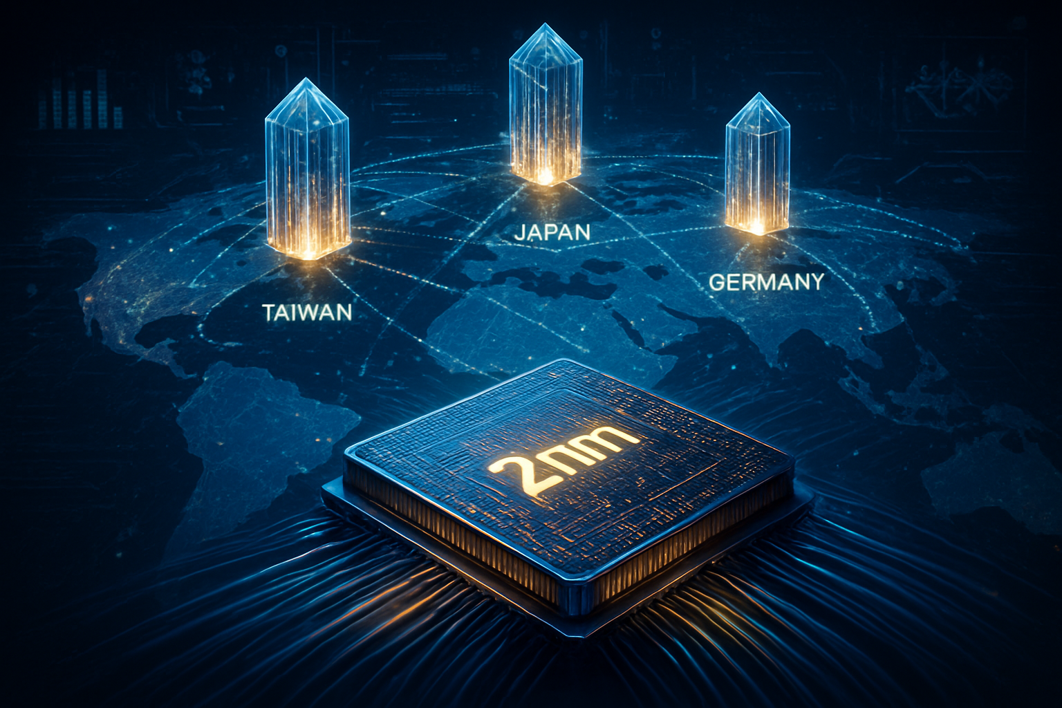
    Looking ahead, the semiconductor sector shows no signs of slowing down. The most anticipated development for 2026 is the transition to mass production of 2nm chips. TSMC has already begun accepting orders for its 2nm process, with Apple (NASDAQ: AAPL) and NVIDIA expected to be the first in line. This transition will introduce "GAAFET" (Gate-All-Around Field-Effect Transistor) technology, offering a 15% speed improvement and a 30% reduction in power consumption compared to the 3nm node.

    In the near term, the industry will focus on the deployment of HBM4-equipped GPUs and the integration of "Liquid-to-Air" cooling systems in data centers. As power densities per rack exceed 100kW, traditional air cooling is no longer viable, leading to a boom for specialized thermal management companies. Experts predict that the next frontier will be "Optical Interconnects," which use light instead of electricity to move data between chips, potentially solving the final bottleneck in AI scaling.

    The primary challenge remains the geopolitical tension surrounding the semiconductor supply chain. While the "Goldilocks" macro environment has eased financial pressures, the concentration of advanced manufacturing in East Asia remains a systemic risk. Efforts to diversify production to the United States and Europe through the CHIPS Act are progressing, but it will take several more years before these regions can match the scale and efficiency of the existing Asian ecosystem.

    A Historic Milestone for the Silicon Economy

    The semiconductor rally of late 2025 marks a definitive turning point in economic history. It is the moment when "Silicon" officially replaced "Oil" as the world's most vital commodity. The combination of cooling inflation and the explosion of Sovereign AI has created a structural demand for compute that is decoupled from traditional business cycles. For investors, the takeaway is clear: semiconductors are no longer a cyclical "tech play," but the fundamental infrastructure of the 21st-century economy.

    As we move into 2026, the industry's focus will shift from "how many chips can we build?" to "how much power can we find?" The energy constraints of AI factories will likely be the defining narrative of the coming year. For now, however, the "Santa Claus Rally" in chip stocks provides a festive end to a year of extraordinary growth. Investors should keep a close eye on the first batch of 2nm test results from TSMC and the official launch of the Vera Rubin platform in early 2026, as these will be the next major catalysts for the sector.


    This content is intended for informational purposes only and represents analysis of current AI developments.

    TokenRing AI delivers enterprise-grade solutions for multi-agent AI workflow orchestration, AI-powered development tools, and seamless remote collaboration platforms.
    For more information, visit https://www.tokenring.ai/.


    Note: Public companies mentioned include NVIDIA (NASDAQ: NVDA), AMD (NASDAQ: AMD), TSMC (NYSE: TSM), Micron (NASDAQ: MU), ASML (NASDAQ: ASML), ARM (NASDAQ: ARM), Microsoft (NASDAQ: MSFT), Amazon (NASDAQ: AMZN), Meta (NASDAQ: META), Apple (NASDAQ: AAPL), Alphabet/Google (NASDAQ: GOOGL), Samsung (KRX: 005930), and SK Hynix (KRX: 000660).

  • The 1.6T Breakthrough: How MACOM’s Analog Innovations are Powering the 100,000-GPU AI Era

    The 1.6T Breakthrough: How MACOM’s Analog Innovations are Powering the 100,000-GPU AI Era

    As of December 18, 2025, the global race for artificial intelligence supremacy has moved beyond the chip itself and into the very fabric that connects them. With Tier-1 AI labs now deploying "Gigawatt-scale" AI factories featuring upwards of 100,000 GPUs, the industry has hit a critical bottleneck: the "networking wall." To shatter this barrier, MACOM Technology Solutions (NASDAQ: MTSI) has emerged as a linchpin of the modern data center, providing the high-performance analog and mixed-signal semiconductors essential for the transition to 800G and 1.6 Terabit (1.6T) data throughput.

    The immediate significance of MACOM’s recent advancements cannot be overstated. In a year defined by the massive ramp-up of the NVIDIA (NASDAQ: NVDA) Blackwell architecture and the emergence of 200,000-GPU clusters like xAI’s Colossus, the demand for "east-west" traffic—the communication between GPUs—has reached a staggering 80 Petabits per second in some facilities. MACOM’s role in enabling 200G-per-lane connectivity and its pioneering "DSP-free" optical architectures have allowed hyperscalers to scale these clusters while slashing power consumption and latency, two factors that previously threatened to stall the progress of frontier AI models.

    The Technical Frontier: 200G Lanes and the Death of the DSP

    At the heart of MACOM’s 2025 success is the shift to 200G-per-lane technology. While 400G and early 800G networks relied on 100G lanes, the 1.6T era requires doubling that density. MACOM’s recently launched chipset portfolio for 1.6T connectivity includes Transimpedance Amplifiers (TIAs) and laser drivers capable of 212 Gbps per lane. This technical leap is facilitated by MACOM’s proprietary Indium Phosphide (InP) process, which allows for the high-sensitivity photodetectors and high-power Continuous Wave (CW) lasers necessary to maintain signal integrity at these extreme frequencies.

    One of the most disruptive technologies in MACOM’s arsenal is its PURE DRIVE™ Linear Pluggable Optics (LPO) ecosystem. Traditionally, optical modules use a Digital Signal Processor (DSP) to "clean up" the signal, but this adds significant power draw and roughly 200 nanoseconds of latency. In the world of synchronous AI training, where thousands of GPUs must wait for the slowest signal to arrive, 200 nanoseconds is an eternity. MACOM’s LPO solutions remove the DSP entirely, relying on high-performance analog components to maintain signal quality. This reduces module power consumption by up to 50% and slashes latency to under 5 nanoseconds, a feat that has drawn widespread praise from the AI research community for its ability to maximize "GPU utilization" rates.

    Furthermore, MACOM has addressed the physical constraints of the data center with its Active Copper Cable (ACC) solutions. As AI racks become more densely packed, the heat generated by traditional optics becomes unmanageable. MACOM’s linear equalizers allow copper cables to reach distances of up to 2.5 meters at 226 Gbps speeds. This allows for "in-rack" 1.6T connections to remain on copper, which is not only cheaper but also significantly more energy-efficient than optical alternatives, providing a critical "thermal relief valve" for high-density GPU clusters.

    Market Dynamics: The Beneficiaries of the Analog Renaissance

    The strategic positioning of MACOM (NASDAQ: MTSI) has made it a primary beneficiary of the massive CAPEX spending by hyperscalers like Meta (NASDAQ: META), Microsoft (NASDAQ: MSFT), and Google (NASDAQ: GOOGL). As these giants transition their backbones from 400G to 800G and 1.6T, they are increasingly looking for ways to bypass the high costs and power requirements of traditional retimed (DSP-based) modules. MACOM’s architecture-agnostic approach—supporting both retimed and linear configurations—allows it to capture market share regardless of which specific networking standard a hyperscaler adopts.

    In the competitive landscape, MACOM is carving out a unique niche against larger rivals like Broadcom (NASDAQ: AVGO) and Marvell Technology (NASDAQ: MRVL). While Broadcom dominates the switch ASIC market with its Tomahawk 6 series, MACOM provides the essential "front-end" analog components that interface with those switches. The partnership between MACOM’s analog expertise and the latest 102.4 Tbps switch chips has created a formidable ecosystem that is difficult for startups to penetrate. For AI labs, the strategic advantage of using MACOM-powered LPO modules lies in the "Total Cost of Ownership" (TCO); by reducing power by several watts per port across a 100,000-port cluster, a data center operator can save millions in annual electricity and cooling costs.

    Wider Significance: Enabling the Gigawatt-Scale AI Factory

    The rise of MACOM’s technology fits into a broader trend of "Scale-Across" architectures. In 2025, a single data center building often cannot support the 300MW to 500MW required for a 200,000-GPU cluster. This has led to the creation of virtual clusters spread across multiple buildings within a campus. MACOM’s high-performance optics are the "connective tissue" that enables these buildings to communicate with the ultra-low latency required to function as a single unit. Without the signal integrity provided by high-performance analog semiconductors, the latency introduced by distance would cause the entire AI training process to desynchronize.

    However, the rapid scaling of these facilities has also raised concerns. The environmental impact of "Gigawatt-scale" sites is under intense scrutiny. MACOM’s focus on power efficiency via DSP-free optics is not just a technical preference but a necessity for the industry’s survival in a world of limited power grids. Comparing this to previous milestones, the jump from 100G to 1.6T in just a few years represents a faster acceleration of networking bandwidth than at any other point in the history of the internet, driven entirely by the insatiable data appetite of Large Language Models (LLMs).

    Future Outlook: The Road to 3.2T and Beyond

    Looking ahead to 2026, the industry is already eyeing the 3.2 Terabit (3.2T) horizon. At the 2025 Optical Fiber Conference, MACOM showcased preliminary 3.2T transmit solutions utilizing 400G-per-lane data rates. While 1.6T is currently the "bleeding edge," the roadmap suggests that the 400G-per-lane transition will be the next major battleground. To meet these demands, experts predict a shift toward Co-Packaged Optics (CPO), where the optical engine is moved directly onto the switch substrate to further reduce power. MACOM’s expertise in chip-stacked TIAs and photodetectors positions them perfectly for this transition.

    The near-term challenge remains the manufacturing yield of 200G-per-lane components. As frequencies increase, the margin for error in semiconductor fabrication shrinks. However, MACOM’s recent award of CHIPS Act funding for GaN-on-SiC and other advanced materials suggests that they have the federal backing to continue innovating in high-speed RF and power applications. Analysts expect MACOM to reach a $1 billion annual revenue run rate by fiscal 2026, fueled by the continued "multi-year growth cycle" of AI infrastructure.

    Conclusion: The Analog Foundation of Digital Intelligence

    In summary, MACOM Technology Solutions has proven that in an increasingly digital world, the most critical innovations are often analog. By enabling the 1.6T networking cycle and providing the components that make 100,000-GPU clusters viable, MACOM has cemented its place as a foundational player in the AI era. Their success in 2025 highlights a shift in the industry's focus from pure compute power to the efficiency and speed of data movement.

    As we look toward the coming months, watch for the first mass-scale deployments of 1.6T LPO modules in "Blackwell-Ultra" clusters. The ability of these systems to maintain high utilization rates will be the ultimate test of MACOM’s technology. In the history of AI, the transition to 1.6T will likely be remembered as the moment the "networking wall" was finally dismantled, allowing for the training of models with trillions of parameters that were previously thought to be computationally—and logistically—impossible.


    This content is intended for informational purposes only and represents analysis of current AI developments.

    TokenRing AI delivers enterprise-grade solutions for multi-agent AI workflow orchestration, AI-powered development tools, and seamless remote collaboration platforms.
    For more information, visit https://www.tokenring.ai/.

  • The Invisible Backbone of AI: Why Advanced Packaging is the New Battleground for Semiconductor Dominance

    The Invisible Backbone of AI: Why Advanced Packaging is the New Battleground for Semiconductor Dominance

    As the artificial intelligence revolution accelerates into late 2025, the industry’s focus has shifted from the raw transistor counts of chips to the sophisticated architecture that holds them together. While massive Large Language Models (LLMs) continue to demand unprecedented compute power, the primary bottleneck is no longer just the speed of the processor, but the "memory wall"—the physical limit of how fast data can travel between memory and logic. Advanced packaging has emerged as the critical solution to this crisis, transforming from a secondary manufacturing step into the primary frontier of semiconductor innovation.

    At the heart of this transition is Kulicke and Soffa Industries (NASDAQ: KLIC), a company that has successfully pivoted from its legacy as a leader in traditional wire bonding to becoming a pivotal player in the high-stakes world of AI advanced packaging. By enabling the complex stacking and interconnectivity required for High Bandwidth Memory (HBM) and chiplet architectures, KLIC is proving that the future of AI performance will be won not just by the designers of chips, but by the masters of assembly.

    The Technical Leap: Solving the Memory Wall with Fluxless TCB

    The technical challenge of 2025 AI hardware lies in the transition from 2D layouts to 2.5D and 3D heterogeneous architectures. Traditional wire bonding, which uses thin gold or copper wires to connect chips to their packages, is increasingly insufficient for the ultra-high-speed requirements of AI GPUs like the Blackwell series from NVIDIA (NASDAQ: NVDA). These modern accelerators require thousands of microscopic connections, known as micro-bumps, to be placed with sub-10-micron precision. This is where KLIC’s Advanced Solutions segment, specifically its APTURA™ series, has become indispensable.

    KLIC’s breakthrough technology is Fluxless Thermo-Compression Bonding (FTC). Unlike traditional methods that use chemical flux to remove oxidation—a process that leaves behind residues difficult to clean at the fine pitches required for HBM4—KLIC’s FTC uses a formic acid vapor in-situ. This "dry" process ensures a cleaner, more reliable bond, allowing for an interconnect pitch as small as 8 micrometers. This level of precision is vital for the 12- and 16-layer HBM stacks that provide the 4TB/s+ bandwidth necessary for next-generation AI training.

    Furthermore, KLIC has introduced the CuFirst™ Hybrid Bonding technology. While traditional bonding relies on heat and pressure to melt solder bumps, hybrid bonding allows copper-to-copper interconnects at room temperature, followed by a dielectric seal. This "bumpless" approach significantly reduces the distance data must travel, cutting latency and reducing power consumption by up to 40% compared to previous generations. By providing these tools, KLIC is enabling the industry to move beyond the physical limits of traditional silicon scaling, a trend often referred to as "More than Moore."

    Market Impact: Navigating the CoWoS Supply Chain

    The strategic importance of advanced packaging is best reflected in the supply chain of Taiwan Semiconductor Manufacturing Company (NYSE: TSM), the world’s leading foundry. In late 2025, TSMC’s Chip-on-Wafer-on-Substrate (CoWoS) capacity has become the most valuable real estate in the tech world. As TSMC doubled its CoWoS capacity to roughly 80,000 wafers per month to meet the demands of NVIDIA and Advanced Micro Devices (NASDAQ: AMD), the equipment providers that qualify for these lines have seen their market positions solidify.

    KLIC has successfully broken into this elite circle, qualifying its fluxless TCB systems for TSMC’s CoWoS-L process. This has placed KLIC in direct competition with incumbents like ASMPT (HKG: 0522) and BE Semiconductor Industries (AMS: BESI). While ASMPT remains a high-volume leader in the broader market, KLIC’s specialized focus on fluxless technology has made it a preferred partner for the high-yield, high-reliability requirements of AI server modules. For companies like NVIDIA, having multiple qualified equipment vendors like KLIC ensures a more resilient supply chain and helps mitigate the chronic shortages that plagued the industry in 2023 and 2024.

    The shift also benefits AMD, which has been more aggressive in adopting 3D chiplet architectures. AMD’s MI350 series, launched earlier this year, utilizes 3D hybrid bonding to stack compute chiplets directly onto I/O dies. This architectural choice gives AMD a competitive edge in power efficiency, a metric that has become as important as raw speed for data center operators. As these tech giants battle for AI supremacy, their reliance on advanced packaging equipment providers has effectively turned companies like KLIC into the "arms dealers" of the AI era.

    The Wider Significance: Beyond Moore's Law

    The rise of advanced packaging marks a fundamental shift in the semiconductor landscape. For decades, the industry followed Moore’s Law, doubling transistor density every two years by shrinking the size of individual transistors. However, as transistors approach the atomic scale, the cost and complexity of further shrinking have skyrocketed. Advanced packaging offers a way out of this economic trap by allowing engineers to "disaggregate" the chip into smaller, specialized chiplets that can be manufactured on different process nodes and then stitched together.

    This trend has profound geopolitical implications. Under the U.S. CHIPS Act and similar initiatives in Europe and Japan, there is a renewed focus on bringing packaging capabilities back to Western shores. Historically, packaging was seen as a low-margin, labor-intensive "back-end" process that was outsourced to Southeast Asia. In 2025, it is recognized as a high-tech, high-margin "mid-end" process essential for national security and technological sovereignty. KLIC, as a U.S.-headquartered company with a deep global footprint, is uniquely positioned to benefit from this reshoring trend.

    Furthermore, the environmental impact of AI is under intense scrutiny. The energy required to move data between a processor and its memory can often exceed the energy used for the actual computation. By using KLIC’s advanced bonding technologies to place memory closer to the logic, the industry is making significant strides in "Green AI." Reducing the parasitic capacitance of interconnects is no longer just a technical goal; it is a sustainability mandate for the world's largest data center operators.

    Future Outlook: The Road to Glass Substrates and CPO

    Looking toward 2026 and 2027, the roadmap for advanced packaging includes even more radical shifts. One of the most anticipated developments is the move from organic substrates to glass substrates. Glass offers superior flatness and thermal stability, which will be necessary as AI chips grow larger and hotter. Companies like KLIC are already in R&D phases for equipment that can handle the unique handling and bonding requirements of glass, which is far more brittle than the materials used today.

    Another major horizon is Co-Packaged Optics (CPO). As electrical signals struggle to maintain integrity over longer distances, the industry is looking to integrate optical fibers directly into the chip package. This would allow data to be transmitted via light rather than electricity, virtually eliminating the "memory wall" and enabling massive clusters of GPUs to act as a single, giant processor. The precision required to align these optical fibers is an order of magnitude higher than even today’s most advanced TCB, representing the next great challenge for KLIC’s engineering teams.

    Experts predict that by 2027, the "Year of HBM4," hybrid bonding will move from niche applications into high-volume manufacturing. While TCB remains the workhorse for today's Blackwell and MI350 chips, the transition to hybrid bonding will require a massive new cycle of capital expenditure. The winners will be those who can provide high-throughput machines that maintain sub-micron accuracy in a high-volume factory environment.

    A New Era of Semiconductor Assembly

    The transformation of Kulicke and Soffa from a wire-bonding specialist into an advanced packaging powerhouse is a microcosm of the broader shift in the semiconductor industry. As AI models grow in complexity, the "package" has become as vital as the "chip." The ability to stack, connect, and cool these massive silicon systems is now the primary determinant of who leads the AI race.

    Key takeaways from this development include the critical role of fluxless bonding in improving yields for HBM4 and the strategic importance of being qualified in the TSMC CoWoS supply chain. As we move further into 2026, the industry will be watching for the first high-volume applications of glass substrates and the continued adoption of hybrid bonding.

    For investors and industry observers, the message is clear: the next decade of AI breakthroughs will not just be written in code or silicon, but in the microscopic copper interconnects that bind them together. Advanced packaging is no longer the final step in the process; it is the foundation upon which the future of artificial intelligence is being built.


    This content is intended for informational purposes only and represents analysis of current AI developments.

    TokenRing AI delivers enterprise-grade solutions for multi-agent AI workflow orchestration, AI-powered development tools, and seamless remote collaboration platforms.
    For more information, visit https://www.tokenring.ai/.
  • The HBM Supercycle: How the AI Memory Boom is Redefining Silicon Architecture and Lifting Equipment Giants

    The HBM Supercycle: How the AI Memory Boom is Redefining Silicon Architecture and Lifting Equipment Giants

    As the artificial intelligence revolution enters its most capital-intensive phase, the industry's focus has shifted from the raw processing power of GPUs to the critical bottleneck of data movement. High Bandwidth Memory (HBM) has emerged as the "fuel" of the AI era, transforming from a niche specialized component into the single most influential driver of the semiconductor supply chain. By late 2025, the demand for these dense, vertically stacked memory chips has reached a fever pitch, creating a massive windfall for the equipment manufacturers that provide the precision tools necessary to build them.

    Leading this charge is Lam Research (NASDAQ: LRCX), which has seen its valuation and order books swell as chipmakers race to solve the "memory wall." The current transition from HBM3E to the next-generation HBM4 standard represents more than just a capacity upgrade; it is a fundamental shift in how memory and logic are integrated. As AI models grow to trillions of parameters, the ability to feed data to processors like NVIDIA (NASDAQ: NVDA) Blackwell and Rubin chips has become the primary differentiator in the race for AI supremacy, making the equipment used to etch and plate these chips more valuable than ever.

    The Architecture War: From HBM3E to HBM4

    The technical landscape of AI memory in late 2025 is defined by the transition from the "capacity war" of HBM3E to the "architecture war" of HBM4. While 12-layer HBM3E remains the current workhorse for data center deployments, the industry has begun the shift toward 16-layer HBM4, which was standardized by JEDEC earlier this year. HBM4 is a landmark development because it doubles the interface width to 2048-bit, allowing for bandwidths exceeding 1.5 TB/s per stack. This leap is necessitated by the massive data throughput requirements of next-generation AI training clusters, which are increasingly limited by the energy and time required to move data between the processor and memory.

    To achieve these specifications, manufacturers are relying on advanced Through-Silicon Via (TSV) technology, where thousands of microscopic holes are drilled through silicon layers to create vertical electrical connections. Lam Research has solidified its position as the gatekeeper of this process with its new Akara™ etching system. Unlike previous generations, HBM4 requires deeper, narrower vias with virtually zero "scalloping" or roughness on the interior walls. Lam’s Syndion and Akara tools provide the high-aspect-ratio etching needed to stack 16 or even 20 layers of DRAM while maintaining electrical integrity. This is complemented by the SABRE 3D® deposition system, which handles the copper electrofilling of these vias, ensuring void-free connections that are essential for high-yield production.

    Initial reactions from the AI research community have been overwhelmingly positive, though tempered by the sheer complexity of the manufacturing process. Experts note that HBM4 marks the first time the "base die"—the bottom layer of the memory stack—is being manufactured on advanced logic nodes (such as 5nm or 12nm) rather than traditional memory processes. This allows the memory stack to handle more complex logic functions, such as error correction and power management, directly on the chip. However, this integration has introduced significant thermal challenges, as stacking logic and memory together creates "hot spots" that can lead to performance throttling if not managed by advanced packaging techniques.

    Market Dynamics and the Rise of the Equipment Giants

    The financial implications of this memory boom are most visible in the balance sheets of wafer fabrication equipment (WFE) providers. In its October 2025 earnings report, Lam Research posted record Q3 revenue of $5.32 billion, a nearly 28% increase year-over-year. Management highlighted that HBM-related revenue grew by 50% during the same period, far outstripping the growth of the broader semiconductor market. For every dollar invested in AI data centers, a growing percentage is now flowing directly into the specialized etching and deposition tools required for 3D stacking. This has placed Lam Research, along with competitors like Applied Materials (NASDAQ: AMAT) and Tokyo Electron (TYO: 8035), at the center of the AI investment thesis.

    In the competitive landscape of memory producers, SK Hynix (KRX: 000660) continues to hold the lion's share of the HBM market, estimated at over 60% as of late 2025. Their "trilateral alliance" with NVIDIA and TSMC (NYSE: TSM) has become the gold standard for AI hardware, utilizing TSMC’s logic process for the HBM4 base die. Meanwhile, Micron (NASDAQ: MU) has successfully climbed to the number two spot, capturing roughly 22% of the market by aggressively scaling its HBM3E production. Samsung (KRX: 005930), while trailing in market share at 16%, is betting heavily on its "all-in-one" capability—acting as the memory maker, foundry, and packager—to regain ground as HBM4 moves into mass production in 2026.

    This shift is disrupting the traditional "commodity" nature of the memory market. HBM is no longer a generic part bought in bulk; it is a highly customized, co-designed component that requires deep collaboration between the memory maker and the logic designer (like NVIDIA or AMD). This strategic advantage favors companies that can master the complex packaging and integration steps, effectively raising the barrier to entry and securing long-term supply agreements that were previously unheard of in the volatile DRAM industry.

    The Wider Significance: Breaking the Memory Wall

    The HBM boom represents a pivotal moment in the history of computing, signaling a move from "compute-centric" to "data-centric" architecture. For decades, processor speeds increased much faster than memory bandwidth, leading to the "memory wall" where CPUs and GPUs spent most of their time waiting for data. By bringing memory physically closer to the logic and stacking it vertically, the industry is effectively trying to collapse the distance data must travel. This is not just about speed; it is about power efficiency. In 2025, data movement accounts for a significant portion of the energy consumed by AI models, and HBM4’s wider interface allows for lower clock speeds at higher bandwidths, significantly reducing the energy-per-bit transferred.

    However, this advancement comes with concerns regarding supply chain concentration and cost. The extreme precision required by Lam Research's tools and the low yields associated with 16-layer stacking have kept HBM prices high. This has led to a "compute divide," where only the largest tech giants—the so-called "Hyperscalers"—can afford the massive HBM-laden clusters required to train the next generation of frontier models. Critics argue that this concentration of hardware power could stifle innovation among smaller startups and academic institutions that cannot compete with the capital expenditures of companies like Microsoft (NASDAQ: MSFT) or Meta (NASDAQ: META).

    Furthermore, the integration of memory and logic via HBM4 is a precursor to "Processing-in-Memory" (PIM), where simple calculations are performed within the memory stack itself. This would represent the most significant change in computer architecture since the von Neumann model, potentially allowing AI models to run with orders of magnitude less power. The success of HBM today is the foundational step toward this more radical future.

    Future Horizons: Hybrid Bonding and Beyond

    Looking ahead to 2026 and 2027, the industry is preparing for the next major technical hurdle: the transition to hybrid bonding. Currently, most HBM4 stacks use advanced micro-bumping (solder balls) to connect layers. However, as stacks move toward 20 layers and beyond, these bumps become too large and introduce too much thermal resistance. Hybrid bonding—a process that bonds copper pads directly to copper pads without solder—is expected to be the key to HBM5. This will require even more sophisticated equipment from Lam Research and its peers, as the surfaces must be perfectly flat and clean at an atomic level to bond successfully.

    We also expect to see the emergence of "custom HBM," where major AI players like Google (NASDAQ: GOOGL) or Amazon (NASDAQ: AMZN) design their own proprietary base dies for HBM stacks to optimize for their specific AI workloads. This would further entrench the relationship between foundries like TSMC and memory makers, while simultaneously increasing the demand for the specialized WFE tools that enable such high-level customization. The primary challenge will remain thermal management; as stacks get taller and more integrated, cooling the middle layers of the "silicon sandwich" will require innovations in liquid cooling and new thermal interface materials.

    A New Era for Semiconductors

    The AI memory boom has fundamentally rewritten the rules of the semiconductor industry. What was once a cyclical commodity business has transformed into a high-margin, high-tech arms race. Lam Research’s emergence as a central player in this narrative underscores the reality that the future of AI is as much a feat of mechanical and chemical engineering as it is of software and algorithms. The ability to etch vias and plate copper at the nanometer scale is now just as critical to the development of AGI as the neural network architectures themselves.

    In summary, the transition to HBM4 and the massive expansion of 3D stacking are the primary drivers of the current semiconductor supercycle. As we move into 2026, the industry will be watching for the first successful mass-production runs of 16-layer stacks and the initial implementation of hybrid bonding. For investors and tech enthusiasts alike, the "memory wall" is no longer just a theoretical hurdle—it is the most lucrative and technically challenging frontier in modern technology.


    This content is intended for informational purposes only and represents analysis of current AI developments.

    TokenRing AI delivers enterprise-grade solutions for multi-agent AI workflow orchestration, AI-powered development tools, and seamless remote collaboration platforms.
    For more information, visit https://www.tokenring.ai/.
  • The H200 Pivot: Nvidia Navigates a $30 Billion Opening Amid Impending 2026 Tariff Wall

    The H200 Pivot: Nvidia Navigates a $30 Billion Opening Amid Impending 2026 Tariff Wall

    In a move that has sent shockwaves through both Silicon Valley and Beijing, the geopolitical landscape for artificial intelligence has shifted dramatically as of December 2025. Following a surprise one-year waiver announced by the U.S. administration on December 8, 2025, Nvidia (NASDAQ: NVDA) has been granted permission to resume sales of its high-performance H200 Tensor Core GPUs to "approved customers" in China. This reversal marks a pivotal moment in the U.S.-China "chip war," transitioning from a strategy of total containment to a "transactional diffusion" model that allows the flow of high-end hardware in exchange for direct revenue sharing with the U.S. Treasury.

    The immediate significance of this development cannot be overstated. For the past year, Chinese tech giants have been forced to rely on "crippled" versions of Nvidia hardware, such as the H20, which were intentionally slowed to meet strict export controls. The lifting of these restrictions for the H200—the flagship of Nvidia’s Hopper architecture—grants Chinese firms the raw computational power required to train frontier-level large language models (LLMs) that were previously out of reach. However, this opportunity comes with a massive caveat: a looming "tariff cliff" in November 2026 and a mandatory 25% revenue-sharing fee that threatens to squeeze Nvidia’s legendary profit margins.

    Technical Rebirth: From the Crippled H20 to the Flagship H200

    The technical disparity between what Nvidia was allowed to sell in China and what it can sell now is staggering. The previous China-specific chip, the H20, was engineered to fall below the U.S. government’s "Total Processing Performance" (TPP) threshold, resulting in an AI performance of approximately 148 TFLOPS (FP8). In contrast, the H200 delivers a massive 1,979 TFLOPS—nearly 13 times the performance of its predecessor. This jump is critical because while the H20 was capable of "inference" (running existing AI models), it lacked the brute force necessary for "training" the next generation of generative AI models from scratch.

    Beyond raw compute, the H200 features 141GB of HBM3e memory and 4.8 TB/s of bandwidth, providing a 20% increase in data throughput over the standard H100. This specification is particularly vital for the massive datasets used by companies like Alibaba (NYSE: BABA) and Baidu (NASDAQ: BIDU). Industry experts note that the H200 is the first "frontier-class" chip to enter the Chinese market legally since the 2023 lockdowns. While Nvidia’s newer Blackwell (B200) and upcoming Rubin architectures remain strictly prohibited, the H200 provides a "Goldilocks" solution: powerful enough to keep Chinese firms dependent on the Nvidia ecosystem, but one generation behind the absolute cutting edge reserved for U.S. and allied interests.

    Market Dynamics: A High-Stakes Game for Tech Giants

    The reopening of the Chinese market for H200s is expected to be a massive revenue driver for Nvidia, with analysts at Wells Fargo (NYSE: WFC) estimating a $25 billion to $30 billion annual opportunity. This development puts immediate pressure on domestic Chinese chipmakers like Huawei, whose Ascend 910C had been gaining significant traction as the only viable alternative for Chinese firms. With the H200 back on the table, many Chinese cloud providers may pivot back to Nvidia’s superior software stack, CUDA, potentially stalling the momentum of China's domestic semiconductor self-sufficiency.

    However, the competitive landscape is complicated by the "25% revenue-sharing fee" imposed by the U.S. government. For every H200 sold in China, Nvidia must pay a quarter of the revenue directly to the U.S. Treasury. This creates a strategic dilemma for Nvidia: if they pass the cost entirely to customers, the chips may become too expensive compared to Huawei’s offerings; if they absorb the cost, their industry-leading margins will take a significant hit. Competitors like Advanced Micro Devices (NASDAQ: AMD) are also expected to seek similar waivers for their MI300 series, potentially leading to a renewed price war within the restricted Chinese market.

    The Geopolitical Gamble: Transactional Diffusion and the 2026 Cliff

    This policy shift represents a new phase in global AI governance. By allowing H200 sales, the U.S. is betting that it can maintain a "strategic lead" through software and architecture (keeping Blackwell and Rubin exclusive) while simultaneously draining capital from Chinese tech firms. This "transactional diffusion" strategy uses Nvidia’s hardware as a diplomatic and economic tool. Yet, the broader AI landscape remains volatile due to the "Chip-for-Chip" tariff policy slated for full implementation on November 10, 2026.

    The 2026 tariffs act as a sword of Damocles hanging over the industry. If China does not meet specific purchase quotas for U.S. goods by late 2026, reciprocal tariffs could rise by another 10% to 20%. This creates a "revenue cliff" where Chinese firms are currently incentivized to aggressively stockpile H200s throughout the first three quarters of 2026 before the trade barriers potentially snap shut. Concerns remain that this "boom and bust" cycle could lead to significant market volatility and a repeat of the inventory write-downs Nvidia faced in early 2025.

    Future Outlook: The Race to November 2026

    In the near term, expect a massive surge in Nvidia’s Data Center revenue as Chinese hyperscalers rush to secure H200 allocations. This "pre-tariff pull-forward" will likely inflate Nvidia's earnings throughout the first half of 2026. However, the long-term challenge remains the development of "sovereign AI" in China. Experts predict that Chinese firms will use the H200 window to accelerate their software optimization, making their models less dependent on specific hardware architectures in preparation for a potential total ban in 2027.

    The next twelve months will also see a focus on supply chain resilience. As 2026 approaches, Nvidia and its manufacturing partner Taiwan Semiconductor Manufacturing Company (NYSE: TSM) will likely face increased pressure to diversify assembly and packaging outside of the immediate conflict zones in the Taiwan Strait. The success of the H200 waiver program will serve as a litmus test for whether "managed competition" can coexist with the intense national security concerns surrounding artificial intelligence.

    Conclusion: A Delicate Balance in the AI Age

    The lifting of the H200 ban is a calculated risk that underscores Nvidia’s central role in the global economy. By navigating the dual pressures of U.S. regulatory fees and the impending 2026 tariff wall, Nvidia is attempting to maintain its dominance in the world’s second-largest AI market while adhering to an increasingly complex set of geopolitical rules. The H200 provides a temporary bridge for Chinese AI development, but the high costs and looming deadlines ensure that the "chip war" is far from over.

    As we move through 2026, the key indicators to watch will be the adoption rate of the H200 among Chinese state-owned enterprises and the progress of the U.S. Treasury's revenue-collection mechanism. This development is a landmark in AI history, representing the first time high-end AI compute has been used as a direct instrument of fiscal and trade policy. For Nvidia, the path forward is a narrow one, balanced between unprecedented opportunity and the very real threat of a geopolitical "cliff" just over the horizon.


    This content is intended for informational purposes only and represents analysis of current AI developments.

    TokenRing AI delivers enterprise-grade solutions for multi-agent AI workflow orchestration, AI-powered development tools, and seamless remote collaboration platforms.
    For more information, visit https://www.tokenring.ai/.
  • The High-NA Frontier: ASML Solidifies the Sub-2nm Era as EUV Adoption Hits Critical Mass

    The High-NA Frontier: ASML Solidifies the Sub-2nm Era as EUV Adoption Hits Critical Mass

    As of late 2025, the semiconductor industry has reached a historic inflection point, driven by the successful transition of High-Numerical Aperture (High-NA) Extreme Ultraviolet (EUV) lithography from experimental labs to the factory floor. ASML (NASDAQ: ASML), the world’s sole provider of the machinery required to print the world’s most advanced chips, has officially entered the high-volume manufacturing (HVM) phase for its next-generation systems. This milestone marks the beginning of the sub-2nm era, providing the essential infrastructure for the next decade of artificial intelligence, high-performance computing, and mobile technology.

    The immediate significance of this development cannot be overstated. With the shipment of the Twinscan EXE:5200B to major foundries, the industry has solved the "stitching" and throughput challenges that once threatened to stall Moore’s Law. For ASML, the successful ramp of these multi-hundred-million-dollar machines is the primary engine behind its projected 2030 revenue targets of up to €60 billion. As logic and DRAM manufacturers race to integrate these tools, the gap between those who can afford the "bleeding edge" and those who cannot has never been wider.

    Breaking the Sub-2nm Barrier: The Technical Triumph of High-NA

    The technical centerpiece of ASML’s 2025 success is the EXE:5200B, a machine that represents the pinnacle of human engineering. Unlike standard EUV tools, which use a 0.33 Numerical Aperture (NA) lens, High-NA systems utilize a 0.55 NA anamorphic lens system. This allows for a significantly higher resolution, enabling chipmakers to print features as small as 8nm—a requirement for the 1.4nm (A14) and 1nm nodes. By late 2025, ASML has successfully boosted the throughput of these systems to 175–200 wafers per hour (wph), matching the productivity of previous generations while drastically reducing the need for "multi-patterning."

    One of the most significant technical hurdles overcome this year was "reticle stitching." Because High-NA lenses are anamorphic (magnifying differently in the X and Y directions), the field size is halved compared to standard EUV. This required engineers to "stitch" two halves of a chip design together with nanometer precision. Reports from IMEC and Intel (NASDAQ: INTC) in mid-2025 confirmed that this process has stabilized, allowing for the production of massive AI accelerators that exceed traditional size limits. Furthermore, the industry has begun transitioning to Metal Oxide Resists (MOR), which are thinner and more sensitive than traditional chemically amplified resists, allowing the High-NA light to be captured more effectively.

    Initial reactions from the research community have been overwhelmingly positive, with experts noting that High-NA reduces the number of process steps by over 40 on critical layers. This reduction in complexity is vital for yield management at the 1.4nm node. While the sheer cost of the machines—estimated at over $380 million each—initially caused hesitation, the data from 2025 pilot lines has proven that the reduction in mask sets and processing time makes High-NA a cost-effective solution for the highest-volume, highest-performance chips.

    The Foundry Arms Race: Intel, TSMC, and Samsung Diverge

    The adoption of High-NA has created a strategic divide among the "Big Three" chipmakers. Intel has emerged as the most aggressive pioneer, having fully installed two production-grade EXE:5200 units at its Oregon facility by late 2025. Intel is betting its entire "Intel 14A" roadmap on being the first to market with High-NA, aiming to reclaim the crown of process leadership from TSMC (NYSE: TSM). For Intel, the strategic advantage lies in early mastery of the tool’s quirks, potentially allowing them to offer 1.4nm capacity to external foundry customers before their rivals.

    TSMC, conversely, has maintained a pragmatic stance for much of 2025, focusing on its N2 and A16 nodes using standard EUV with multi-patterning. However, the tide shifted in late 2025 when reports surfaced that TSMC had placed significant orders for High-NA machines to support its A14P node, expected to ramp in 2027-2028. This move signals that even the most cost-conscious foundry leader recognizes that standard EUV cannot scale indefinitely. Samsung (KRX: 005930) also took delivery of its first production High-NA unit in Q4 2025, intending to use the technology for its SF1.4 node to close the performance gap in the mobile and AI markets.

    The implications for the broader market are profound. Companies like NVIDIA (NASDAQ: NVDA) and Apple (NASDAQ: AAPL) are now forced to navigate this fragmented landscape, deciding whether to stick with TSMC’s proven 0.33 NA methods or pivot to Intel’s High-NA-first approach for their next-generation AI GPUs and silicon. This competition is driving a "supercycle" for ASML, as every major player is forced to buy the most expensive equipment just to stay in the race, further cementing ASML’s monopoly at the top of the supply chain.

    Beyond Logic: EUV’s Critical Role in DRAM and Global Trends

    While logic manufacturing often grabs the headlines, 2025 has been the year EUV became indispensable for memory. The mass production of "1c" (12nm-class) DRAM is now in full swing, with SK Hynix (KRX: 000660) leading the charge by utilizing five to six EUV layers for its HBM4 (High Bandwidth Memory) products. Even Micron (NASDAQ: MU), which was famously the last major holdout for EUV technology, has successfully ramped its 1-gamma node using EUV at its Hiroshima plant this year. The integration of EUV in DRAM is critical for ASML’s long-term margins, as memory manufacturers typically purchase tools in higher volumes than logic foundries.

    This shift fits into a broader global trend: the AI Supercycle. The explosion in demand for generative AI has created a bottomless appetite for high-density memory and high-performance logic, both of which now require EUV. However, this growth is occurring against a backdrop of geopolitical complexity. ASML has reported that while demand from China has normalized—dropping to roughly 20% of revenue from nearly 50% in 2024 due to export restrictions—the global demand for advanced tools has more than compensated. ASML’s gross margin targets of 56% to 60% by 2030 are predicated on this shift toward higher-value High-NA systems and the expansion of EUV into the memory sector.

    Comparisons to previous milestones, such as the initial move from DUV to EUV in 2018, suggest that we are entering a "harvesting" phase. The foundational science is settled, and the focus has shifted to industrialization and yield optimization. The potential concern remains the "cost wall"—the risk that only a handful of companies can afford to design chips at the 1.4nm level, potentially centralizing the AI industry even further into the hands of a few tech giants.

    The Roadmap to 2030: From High-NA to Hyper-NA

    Looking ahead, ASML is already laying the groundwork for the next decade with "Hyper-NA" lithography. As High-NA carries the industry through the 1.4nm and 1nm eras, the subsequent generation of transistors—likely based on Complementary FET (CFET) architectures—will require even higher resolution. ASML’s roadmap for the HXE series targets a 0.75 NA, which would be the most significant jump in optical capability in the company's history. Pilot systems for Hyper-NA are currently projected for introduction around 2030.

    The challenges for Hyper-NA are daunting. At 0.75 NA, the depth of focus becomes extremely shallow, and light polarization effects can degrade image contrast. ASML is currently researching specialized polarization filters and even more advanced photoresist materials to combat these physics-based limitations. Experts predict that the move to Hyper-NA will be as difficult as the original transition to EUV, requiring a complete overhaul of the mask and pellicle ecosystem. However, if successful, it will extend the life of silicon-based computing well into the 2030s.

    In the near term, the industry will focus on the "A14" ramp. We expect to see the first silicon samples from Intel’s High-NA lines by mid-2026, which will be the ultimate test of whether the technology can deliver on its promise of superior power, performance, and area (PPA). If Intel succeeds in hitting its yield targets, it could trigger a massive wave of "FOMO" (fear of missing out) among other chipmakers, leading to an even faster adoption rate for ASML’s most advanced tools.

    Conclusion: The Indispensable Backbone of AI

    The status of ASML and EUV lithography at the end of 2025 confirms one undeniable truth: the future of artificial intelligence is physically etched by a single company in Veldhoven. The successful deployment of High-NA lithography has effectively moved the goalposts for Moore’s Law, ensuring that the roadmap to sub-2nm chips is not just a theoretical possibility but a manufacturing reality. ASML’s ability to maintain its technological lead while expanding its margins through logic and DRAM adoption has solidified its position as the most critical node in the global technology supply chain.

    As we move into 2026, the industry will be watching for the first "High-NA chips" to enter the market. The success of these products will determine the pace of the next decade of computing. For now, ASML has proven that it can meet the moment, providing the tools necessary to build the increasingly complex brains of the AI era. The "High-NA Era" has officially arrived, and with it, a new chapter in the history of human innovation.


    This content is intended for informational purposes only and represents analysis of current AI developments.

    TokenRing AI delivers enterprise-grade solutions for multi-agent AI workflow orchestration, AI-powered development tools, and seamless remote collaboration platforms.
    For more information, visit https://www.tokenring.ai/.

  • The Silicon Bedrock: Strengthening Forecasts for AI Chip Equipment Signal a Multi-Year Infrastructure Supercycle

    The Silicon Bedrock: Strengthening Forecasts for AI Chip Equipment Signal a Multi-Year Infrastructure Supercycle

    As 2025 draws to a close, the semiconductor industry is witnessing a historic shift in capital allocation, driven by a "giga-cycle" of investment in artificial intelligence infrastructure. According to the latest year-end reports from industry authority SEMI and leading equipment manufacturers, global Wafer Fab Equipment (WFE) spending is forecast to hit a record-breaking $145 billion in 2026. This surge is underpinned by an insatiable demand for next-generation AI processors and high-bandwidth memory, forcing a radical retooling of the world’s most advanced fabrication facilities.

    The immediate significance of this development cannot be overstated. We are moving past the era of "AI experimentation" into a phase of "AI industrialization," where the physical limits of silicon are being pushed by revolutionary new architectures. Leaders in the space, most notably Applied Materials (NASDAQ: AMAT), have reported record annual revenues of over $28 billion for fiscal 2025, with visibility into customer factory plans extending well into 2027. This strengthening forecast suggests that the "pick and shovel" providers of the AI gold rush are entering their most profitable era yet, as the industry races toward a $1 trillion total market valuation by 2026.

    The Architecture of Intelligence: GAA, High-NA, and Backside Power

    The technical backbone of this 2026 supercycle rests on three primary architectural inflections: Gate-All-Around (GAA) transistors, Backside Power Delivery (BSPDN), and High-NA EUV lithography. Unlike the FinFET transistors that dominated the last decade, GAA nanosheets wrap the gate around all four sides of the channel, providing superior control over current leakage and enabling the jump to 2nm and 1.4nm process nodes. Applied Materials has positioned itself as the dominant force here, capturing over 50% market share in GAA-specific equipment, including the newly unveiled Centura Xtera Epi system, which is critical for the epitaxial growth required in these complex 3D structures.

    Simultaneously, the industry is adopting Backside Power Delivery, a radical redesign that moves the power distribution network to the rear of the silicon wafer. This decoupling of power and signal routing significantly reduces voltage drop and clears "routing congestion" on the front side, allowing for denser, more energy-efficient AI chips. To inspect these buried structures, the industry has turned to advanced metrology tools like the PROVision 10 eBeam from Applied Materials, which can "see" through multiple layers of silicon to ensure alignment at the atomic scale.

    Furthermore, the long-awaited era of High-NA (Numerical Aperture) EUV lithography has officially transitioned from the lab to the fab. As of December 2025, ASML (NASDAQ: ASML) has confirmed that its EXE:5200 series machines have completed acceptance testing at Intel (NASDAQ: INTC) and are being delivered to Samsung (KRX: 005930) for 2nm mass production. These €350 million machines allow for finer resolution than ever before, eliminating the need for complex multi-patterning steps and streamlining the production of the massive die sizes required for next-gen AI accelerators like Nvidia’s upcoming Rubin architecture.

    The Equipment Giants: Strategic Advantages and Market Positioning

    The strengthening forecasts have created a clear hierarchy of beneficiaries among the "Big Five" equipment makers. Applied Materials (NASDAQ: AMAT) has successfully pivoted its business model, reducing its exposure to the volatile Chinese market while doubling down on materials engineering for advanced packaging. By dominating the "die-to-wafer" hybrid bonding market with its Kinex system, AMAT is now essential for the production of High-Bandwidth Memory (HBM4), which is expected to see a massive ramp-up in the second half of 2026.

    Lam Research (NASDAQ: LRCX) has similarly fortified its position through its Cryo 3.0 cryogenic etching technology. Originally designed for 3D NAND, this technology has become a bottleneck-breaker for HBM4 production. By etching through-silicon vias (TSVs) at temperatures as low as -80°C, Lam’s tools can achieve near-perfect vertical profiles at 2.5 times the speed of traditional methods. This efficiency is vital as memory makers like SK Hynix (KRX: 000660) report that their 2026 HBM4 capacity is already fully committed to major AI clients.

    For the fabless giants and foundries, these developments represent both an opportunity and a strategic risk. While Nvidia (NASDAQ: NVDA) and Advanced Micro Devices (NASDAQ: AMD) stand to benefit from the higher performance of 2nm GAA chips, they are increasingly dependent on the production yields of TSMC (NYSE: TSM). The market is closely watching whether the equipment providers can deliver enough tools to meet TSMC’s projected 60% expansion in CoWoS (Chip-on-Wafer-on-Substrate) packaging capacity. Any delay in tool delivery could create a multi-billion dollar revenue gap for the entire AI ecosystem.

    Geopolitics, Energy, and the $1 Trillion Milestone

    The wider significance of this equipment boom extends into the realms of global energy and geopolitics. The shift toward "Sovereign AI"—where nations build their own domestic compute clusters—has decentralized demand. Equipment that was once destined for a few mega-fabs in Taiwan and Korea is now being shipped to new "greenfield" projects in the United States, Japan, and Europe, funded by initiatives like the U.S. CHIPS Act. This geographic diversification is acting as a hedge against regional instability, though it introduces new logistical complexities for equipment maintenance and talent.

    Energy efficiency has also emerged as a primary driver for hardware upgrades. As data center power consumption becomes a political and environmental flashpoint, the transition to Backside Power and GAA transistors is being framed as a "green" necessity. Analysts from Gartner and IDC suggest that while generative AI software may face a "trough of disillusionment" in 2026, the demand for the underlying hardware will remain robust because these newer, more efficient chips are required to make AI economically viable at scale.

    However, the industry is not without its concerns. Experts point to a potential "HBM4 capacity crunch" and the massive power requirements of the 2026 data center build-outs as major friction points. If the electrical grid cannot support the 1GW+ data centers currently on the drawing board, the demand for the chips produced by these expensive new machines could soften. Furthermore, the "small yard, high fence" trade policies of late 2025 continue to cast a shadow over the global supply chain, with new export controls on metrology and lithography components remaining a top-tier risk for CEOs.

    Looking Ahead: The Road to 1.4nm and Optical Interconnects

    Looking beyond 2026, the roadmap for AI chip equipment is already focusing on the 1.4nm node (often referred to as A14). This will likely involve even more exotic materials and the potential integration of optical interconnects directly onto the silicon die. Companies are already prototyping "Silicon Photonics" equipment that would allow chips to communicate via light rather than electricity, potentially solving the "memory wall" that currently limits AI training speeds.

    In the near term, the industry will focus on perfecting "heterogeneous integration"—the art of stacking disparate chips (logic, memory, and I/O) into a single package. We expect to see a surge in demand for specialized "bond alignment" tools and advanced cleaning systems that can handle the delicate 3D structures of HBM4. The challenge for 2026 will be scaling these laboratory-proven techniques to the millions of units required by the hyperscale cloud providers.

    A New Era of Silicon Supremacy

    The strengthening forecasts for AI chip equipment signal that we are in the midst of the most significant technological infrastructure build-out since the dawn of the internet. The transition to GAA transistors, High-NA EUV, and advanced packaging represents a total reimagining of how computing hardware is designed and manufactured. As Applied Materials and its peers report record bookings and expanded margins, it is clear that the "silicon bedrock" of the AI era is being laid with unprecedented speed and capital.

    The key takeaways for the coming year are clear: the 2026 "Giga-cycle" is real, it is materials-intensive, and it is geographically diverse. While geopolitical and energy-related risks remain, the structural shift toward AI-centric compute is providing a multi-year tailwind for the equipment sector. In the coming weeks and months, investors and industry watchers should pay close attention to the delivery schedules of High-NA EUV tools and the yield rates of the first 2nm test chips. These will be the ultimate indicators of whether the ambitious forecasts for 2026 will translate into a new era of silicon supremacy.


    This content is intended for informational purposes only and represents analysis of current AI developments.

    TokenRing AI delivers enterprise-grade solutions for multi-agent AI workflow orchestration, AI-powered development tools, and seamless remote collaboration platforms.
    For more information, visit https://www.tokenring.ai/.

  • The Silicon Engine: How SDV Chips are Turning the Modern Car into a High-Performance Data Center

    The Silicon Engine: How SDV Chips are Turning the Modern Car into a High-Performance Data Center

    The automotive industry has reached a definitive tipping point as of late 2025. The era of the internal combustion engine’s mechanical complexity has been superseded by a new era of silicon-driven sophistication. We are no longer witnessing the evolution of the car; we are witnessing the birth of the "Software-Defined Vehicle" (SDV), where the value of a vehicle is determined more by its lines of code and its central processor than by its horsepower or torque. This shift toward centralized compute architectures is fundamentally redesigning the anatomy of the automobile, effectively turning every new vehicle into a high-performance computer on wheels.

    The immediate significance of this transition cannot be overstated. By consolidating the dozens of disparate electronic control units (ECUs) that once governed individual functions—like windows, brakes, and infotainment—into a single, powerful "brain," automakers can now deliver over-the-air (OTA) updates that improve vehicle safety and performance overnight. For consumers, this means a car that gets better with age; for manufacturers, it represents a radical shift in business models, moving away from one-time hardware sales toward recurring software-driven revenue.

    The Rise of the Superchip: 2,000 TOPS and the Death of the ECU

    The technical backbone of this revolution is a new generation of "superchips" designed specifically for the rigors of automotive AI. Leading the charge is NVIDIA (NASDAQ:NVDA) with its DRIVE Thor platform, which entered mass production earlier this year. Built on the Blackwell GPU architecture, Thor delivers a staggering 2,000 TOPS (Trillion Operations Per Second)—an eightfold increase over its predecessor, Orin. What sets Thor apart is its ability to handle "multi-domain isolation." This allows the chip to simultaneously run the vehicle’s safety-critical autonomous driving systems, the digital instrument cluster, and the AI-powered infotainment system on a single piece of silicon without any risk of one process interfering with another.

    Meanwhile, Qualcomm (NASDAQ:QCOM) has solidified its position with the Snapdragon Ride Elite and Snapdragon Cockpit Elite platforms. Utilizing the custom-built Oryon CPU and an enhanced Hexagon NPU, Qualcomm’s latest offerings have seen a 12x increase in AI performance compared to previous generations. This hardware is already being integrated into 2026 models for brands like Mercedes-Benz (OTC:MBGYY) and Li Auto (NASDAQ:LI). Unlike previous iterations that required separate chips for the dashboard and the driving assists, these new platforms enable a "zonal architecture." In this setup, regional controllers (Front, Rear, Left, Right) aggregate data and power locally before sending it to the central brain, a move that BMW (OTC:BMWYY) claims has reduced wiring weight by 30% in its new "Neue Klasse" vehicles.

    This architecture differs sharply from the legacy "distributed" model. In older cars, if a sensor failed or a feature needed an update, it often required physical access to a specific, isolated ECU. Today’s centralized systems allow for "end-to-end" AI training. Instead of engineers writing thousands of "if-then" rules for every possible driving scenario, the car uses Transformer-based neural networks—similar to those powering Large Language Models (LLMs)—to "reason" through traffic by analyzing millions of hours of driving video. This leap in capability has moved the industry from basic lane-keeping to sophisticated, human-like autonomous navigation.

    The New Power Players: Silicon Giants vs. Traditional Giants

    The shift to SDVs has caused a massive seismic shift in the automotive supply chain. Traditional "Tier 1" suppliers like Bosch and Continental are finding themselves in a fierce battle for relevance as NVIDIA and Qualcomm emerge as the new primary partners for automakers. These silicon giants now command the most critical part of the vehicle's bill of materials, giving them unprecedented leverage over the future of transportation. For Tesla (NASDAQ:TSLA), the strategy remains one of fierce vertical integration. While Tesla’s AI5 (Hardware 5) chip has faced production delays—now expected in mid-2027—the company continues to push the limits of its existing AI4 hardware, proving that software optimization is just as critical as raw hardware power.

    The competitive landscape is also forcing traditional automakers into unexpected alliances. Volkswagen (OTC:VWAGY) made headlines this year with its $5 billion investment in Rivian (NASDAQ:RIVN), a move specifically designed to license Rivian’s advanced zonal architecture and software stack. This highlights a growing divide: companies that can build software in-house, and those that must buy it to survive. Startups like Zeekr (NYSE:ZK) are taking the middle ground, leveraging NVIDIA’s Thor to leapfrog established players and deliver Level 3 autonomous features to the mass market faster than their European and American counterparts.

    This disruption extends to the consumer experience. As cars become software platforms, tech giants like Google and Apple are looking to move beyond simple screen mirroring (like CarPlay) to deeper integration with the vehicle’s operating system. The strategic advantage now lies with whoever controls the "Digital Cockpit." With Qualcomm currently holding a dominant market share in cockpit silicon, they are well-positioned to dictate the future of the in-car user interface, potentially sidelining traditional infotainment developers.

    The "iPhone Moment" for the Automobile

    The broader significance of the SDV chip revolution is often compared to the "iPhone moment" for the mobile industry. Just as the smartphone transitioned from a communication device to a general-purpose computing platform, the car is transitioning from a transportation tool to a mobile living space. The integration of on-device LLMs means that AI assistants—powered by technologies like ChatGPT-4o or Google Gemini—can now handle complex, natural-language commands locally on the car’s chip. This ensures driver privacy and reduces latency, allowing the car to act as a proactive personal assistant that can adjust climate, suggest routes, and even manage the driver’s schedule.

    However, this transition is not without its concerns. The move to centralized compute creates a "single point of failure" risk that engineers are working tirelessly to mitigate through hardware redundancy. There are also significant questions regarding data privacy; as cars collect petabytes of video and sensor data to train their AI models, the question of who owns that data becomes a legal minefield. Furthermore, the environmental impact of manufacturing these advanced 3nm and 5nm chips, and the energy required to power 2,000 TOPS processors in an EV, are challenges that the industry must address to remain truly "green."

    Despite these hurdles, the milestone is clear: we have moved past the era of "assisted driving" into the era of "autonomous reasoning." The use of "Digital Twins" through platforms like NVIDIA Omniverse allows manufacturers to simulate billions of miles of driving in virtual worlds before a car ever touches asphalt. This has compressed development cycles from seven years down to less than three, fundamentally changing the pace of innovation in a century-old industry.

    The Road Ahead: 2nm Silicon and Level 4 Autonomy

    Looking toward the near future, the focus is shifting toward even more efficient silicon. Experts predict that by 2027, we will see the first automotive chips built on 2nm process nodes, offering even higher performance-per-watt. This will be crucial for the widespread rollout of Level 4 autonomy—where the car can handle all driving tasks in specific conditions without human intervention. While Tesla’s upcoming Cybercab is expected to launch on older hardware, the true "unsupervised" future will likely depend on the next generation of AI5 and Thor-class processors.

    We are also on the horizon of "Vehicle-to-Everything" (V2X) communication becoming standard. With the compute power now available on-board, cars will not only "see" the road with their own sensors but will also "talk" to smart city infrastructure and other vehicles to coordinate traffic flow and prevent accidents before they are even visible. The challenge remains the regulatory environment, which has struggled to keep pace with the rapid advancement of AI. Experts predict that 2026 will be a "year of reckoning" for global autonomous driving standards as governments scramble to certify these software-defined brains.

    A New Chapter in AI History

    The rise of SDV chips represents one of the most significant chapters in the history of applied artificial intelligence. We have moved from AI as a digital curiosity to AI as a mission-critical safety system responsible for human lives at 70 miles per hour. The key takeaway is that the car is no longer a static product; it is a dynamic, evolving entity. The successful automakers of the next decade will be those who view themselves as software companies first and hardware manufacturers second.

    As we look toward 2026, watch for the first production vehicles featuring NVIDIA Thor to hit the streets and for the further expansion of "End-to-End" AI models in consumer cars. The competition between the proprietary "walled gardens" of Tesla and the open merchant silicon of NVIDIA and Qualcomm will define the next era of mobility. One thing is certain: the silicon engine has officially replaced the internal combustion engine as the heart of the modern vehicle.


    This content is intended for informational purposes only and represents analysis of current AI developments.

    TokenRing AI delivers enterprise-grade solutions for multi-agent AI workflow orchestration, AI-powered development tools, and seamless remote collaboration platforms.
    For more information, visit https://www.tokenring.ai/.
  • The Great Unbundling of Silicon: How UCIe 3.0 is Powering a New Era of ‘Mix-and-Match’ AI Hardware

    The Great Unbundling of Silicon: How UCIe 3.0 is Powering a New Era of ‘Mix-and-Match’ AI Hardware

    The semiconductor industry has reached a pivotal turning point as the Universal Chiplet Interconnect Express (UCIe) standard enters full commercial maturity. As of late 2025, the release of the UCIe 3.0 specification has effectively dismantled the era of monolithic, "black box" processors, replacing it with a modular "mix and match" ecosystem. This development allows specialized silicon components—known as chiplets—from different manufacturers to be housed within a single package, communicating at speeds that were previously only possible within a single piece of silicon. For the artificial intelligence sector, this represents a massive leap forward, enabling the construction of hyper-specialized AI accelerators that can scale to meet the insatiable compute demands of next-generation large language models (LLMs).

    The immediate significance of this transition cannot be overstated. By standardizing how these chiplets communicate, the industry is moving away from proprietary, vendor-locked architectures toward an open marketplace. This shift is expected to slash development costs for custom AI silicon by up to 40% and reduce time-to-market by nearly a year for many fabless design firms. As the AI hardware race intensifies, UCIe 3.0 provides the "lingua franca" that ensures an I/O die from one vendor can work seamlessly with a compute engine from another, all while maintaining the ultra-low latency required for real-time AI inference and training.

    The Technical Backbone: From UCIe 1.1 to the 64 GT/s Breakthrough

    The technical evolution of the UCIe standard has been rapid, culminating in the August 2025 release of the UCIe 3.0 specification. While UCIe 1.1 focused on basic reliability and health monitoring for automotive and data center applications, and UCIe 2.0 introduced standardized manageability and 3D packaging support, the 3.0 update is a game-changer for high-performance computing. It doubles the data rate to 64 GT/s per lane, providing the massive throughput necessary for the "XPU-to-memory" bottlenecks that have plagued AI clusters. A key innovation in the 3.0 spec is "Runtime Recalibration," which allows links to dynamically adjust power and performance without requiring a system reboot—a critical feature for massive AI data centers that must remain operational 24/7.

    This new standard differs fundamentally from previous approaches like Intel Corporation (NASDAQ: INTC)’s proprietary Advanced Interface Bus (AIB) or Advanced Micro Devices, Inc. (NASDAQ: AMD)’s early Infinity Fabric. While those technologies proved the viability of chiplets, they were "closed loops" that prevented cross-vendor interoperability. UCIe 3.0, by contrast, defines everything from the physical layer (the actual wires and bumps) to the protocol layer, ensuring that a chiplet designed by a startup can be integrated into a larger system-on-chip (SoC) manufactured by a giant like NVIDIA Corporation (NASDAQ: NVDA). Initial reactions from the research community have been overwhelmingly positive, with engineers at the Open Compute Project (OCP) hailing it as the "PCIe moment" for internal chip communication.

    The Competitive Landscape: Giants and Challengers Align

    The shift toward a standardized chiplet ecosystem is creating a new hierarchy among tech giants. Intel Corporation (NASDAQ: INTC) has been the most aggressive proponent, having donated the initial specification to the consortium. Their recent launch of the Granite Rapids-D (Xeon 6 SoC) in early 2025 stands as one of the first high-volume products to fully leverage UCIe for modularity at the edge. Meanwhile, NVIDIA Corporation (NASDAQ: NVDA) has adapted its strategy; while it still champions its proprietary NVLink for high-end GPU clusters, it recently released "UCIe-ready" silicon bridges. These bridges allow customers to build custom AI accelerators that can talk directly to NVIDIA’s Blackwell and upcoming Rubin architectures, effectively turning NVIDIA’s hardware into a platform for third-party innovation.

    Taiwan Semiconductor Manufacturing Company (NYSE: TSM) and Samsung Electronics (KRX: 005930) are currently locked in a "foundry race" to provide the packaging technology that makes UCIe possible. TSMC’s 3DFabric and Samsung’s I-Cube/X-Cube technologies are the physical stages where these mix-and-match chiplets perform. In mid-2025, Samsung successfully demonstrated a 4nm chiplet prototype using IP from Synopsys, Inc. (NASDAQ: SNPS), proving that the "mix and match" dream is now a physical reality. This benefits smaller AI startups and fabless companies, who can now purchase "silicon-proven" UCIe blocks from providers like Cadence Design Systems, Inc. (NASDAQ: CDNS) instead of spending millions to design proprietary interconnect logic from scratch.

    Scaling AI: Efficiency, Cost, and the End of the "Reticle Limit"

    The broader significance of UCIe 3.0 lies in its ability to bypass the "reticle limit"—the physical size limit of a single silicon wafer die. As AI models grow, the chips needed to train them have become so large they are physically impossible to manufacture as a single piece of silicon without massive defects. By breaking the processor into smaller chiplets, manufacturers can achieve much higher yields and lower costs. This fits into the broader AI trend of "heterogeneous computing," where different parts of an AI task are handled by specialized hardware—such as a dedicated matrix multiplication die paired with a high-bandwidth memory (HBM) die and a low-power I/O die.

    However, this transition is not without concerns. The primary challenge remains "Standardized Manageability"—the difficulty of debugging a system when the components come from five different companies. If an AI server fails, determining which vendor’s chiplet caused the error becomes a complex legal and technical nightmare. Furthermore, while UCIe 3.0 provides the physical connection, the software stack required to manage these disparate components is still in its infancy. Despite these hurdles, the move toward UCIe is being compared to the transition from mainframe computers to modular PCs; it is an "unbundling" that democratizes high-performance silicon.

    The Horizon: Optical I/O and the 'Chiplet Store'

    Looking ahead, the near-term focus will be on the integration of Optical Compute Interconnects (OCI). Intel has already demonstrated a fully integrated optical I/O chiplet using UCIe that allows chiplets to communicate via fiber optics at 4TBps over distances up to 100 meters. This effectively turns an entire data center rack into a single, giant "virtual chip." In the long term, experts predict the rise of the "Chiplet Store"—a commercial marketplace where companies can buy pre-manufactured, specialized AI chiplets (like a dedicated "Transformer Engine" or a "Security Enclave") and have them assembled by a third-party packaging house.

    The challenges that remain are primarily thermal and structural. Stacking chiplets in 3D (as supported by UCIe 2.0 and 3.0) creates intense heat pockets that require advanced liquid cooling or new materials like glass substrates. Industry analysts predict that by 2027, more than 80% of all high-end AI processors will be UCIe-compliant, as the cost of maintaining proprietary interconnects becomes unsustainable even for the largest tech companies.

    A New Blueprint for the AI Age

    The maturation of the UCIe standard represents one of the most significant architectural shifts in the history of computing. By providing a standardized, high-speed interface for chiplets, the industry has unlocked a modular future that balances the need for extreme performance with the economic realities of semiconductor manufacturing. The "mix and match" ecosystem is no longer a theoretical concept; it is the foundation upon which the next decade of AI progress will be built.

    As we move into 2026, the industry will be watching for the first "multi-vendor" AI chips to hit the market—processors where the compute, memory, and I/O are sourced from entirely different companies. This development marks the end of the monolithic era and the beginning of a more collaborative, efficient, and innovative period in silicon design. For AI companies and investors alike, the message is clear: the future of hardware is no longer about who can build the biggest chip, but who can best orchestrate the most efficient ecosystem of chiplets.


    This content is intended for informational purposes only and represents analysis of current AI developments.

    TokenRing AI delivers enterprise-grade solutions for multi-agent AI workflow orchestration, AI-powered development tools, and seamless remote collaboration platforms.
    For more information, visit https://www.tokenring.ai/.