In a landmark move to secure the future of American computing power, the U.S. Department of Energy (DOE) officially inaugurated the "Genesis Mission" on December 18, 2025. This massive public-private partnership unites the federal government's scientific arsenal with the industrial might of tech giants including Amazon.com, Inc. (NASDAQ: AMZN), Alphabet Inc. (NASDAQ: GOOGL), and Microsoft Corporation (NASDAQ: MSFT). Framed by the administration as a "Manhattan Project-scale" endeavor, the mission aims to solve the single greatest bottleneck facing the artificial intelligence revolution: the staggering energy consumption of next-generation semiconductors and the data centers that house them.
The Genesis Mission arrives at a critical juncture where the traditional power grid is struggling to keep pace with the exponential growth of AI workloads. By integrating the high-performance computing resources of all 17 DOE National Laboratories with the secure cloud infrastructures of the "Big Three" hyperscalers, the initiative seeks to create a unified national AI science platform. This collaboration is not merely about scaling up; it is a strategic effort to achieve "American Energy Dominance" by leveraging AI to design, license, and deploy radical new energy solutions—ranging from advanced small modular reactors (SMRs) to breakthrough fusion technology—specifically tailored to fuel the AI era.
Technical Foundations: The Architecture of Energy Efficiency
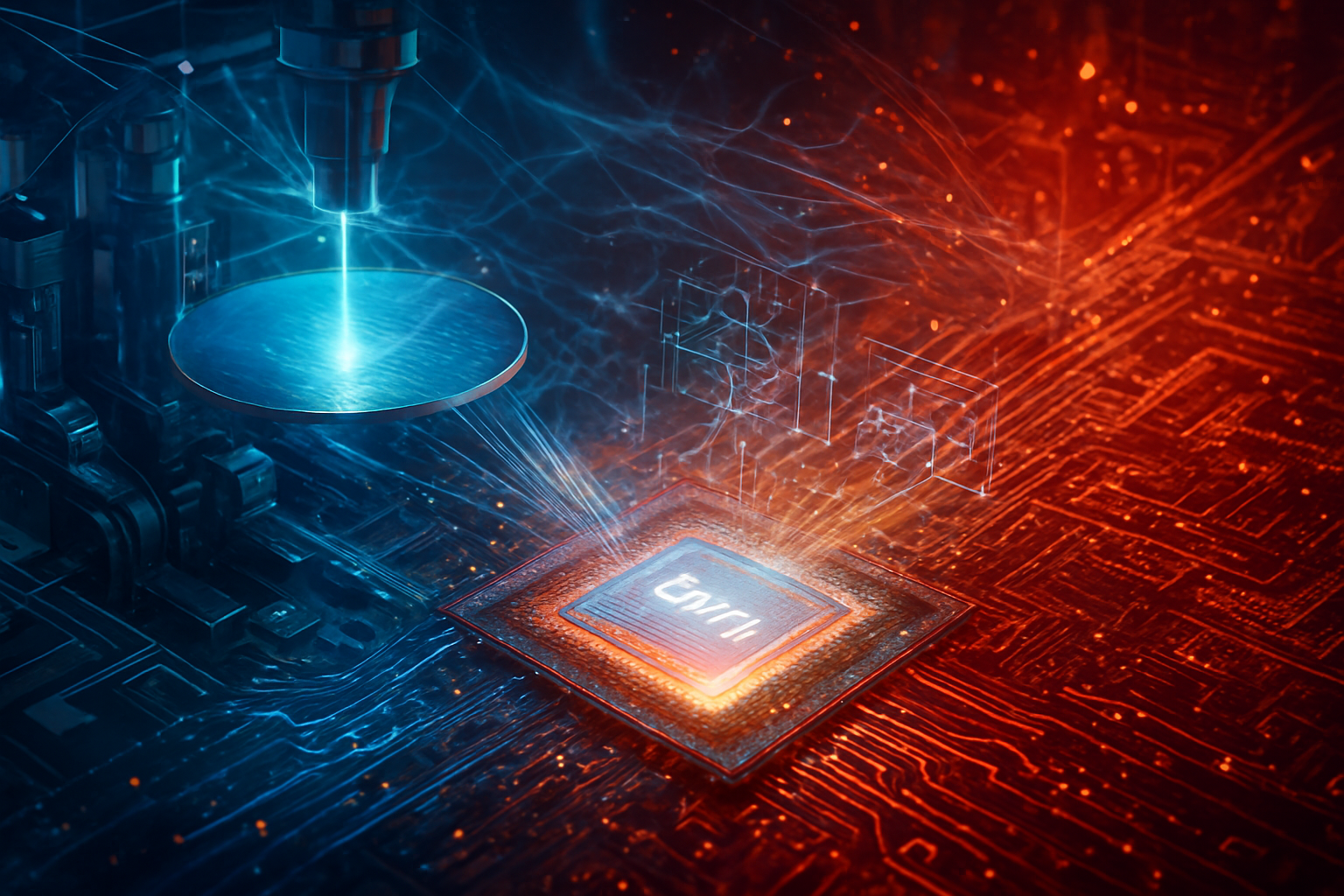
The technical heart of the Genesis Mission is the American Science and Security Platform, a high-security "engine" that bridges federal supercomputers with private cloud environments. Unlike previous efforts that focused on general-purpose computing, the Genesis Mission is specifically optimized for "scientific foundation models." These models are designed to reason through complex physics and chemistry problems, enabling the co-design of microelectronics that are exponentially more efficient. A core component of this is the Microelectronics Energy Efficiency Research Center (MEERCAT), which focuses on developing semiconductors that utilize new materials beyond silicon to reduce power leakage and heat generation in AI training clusters.
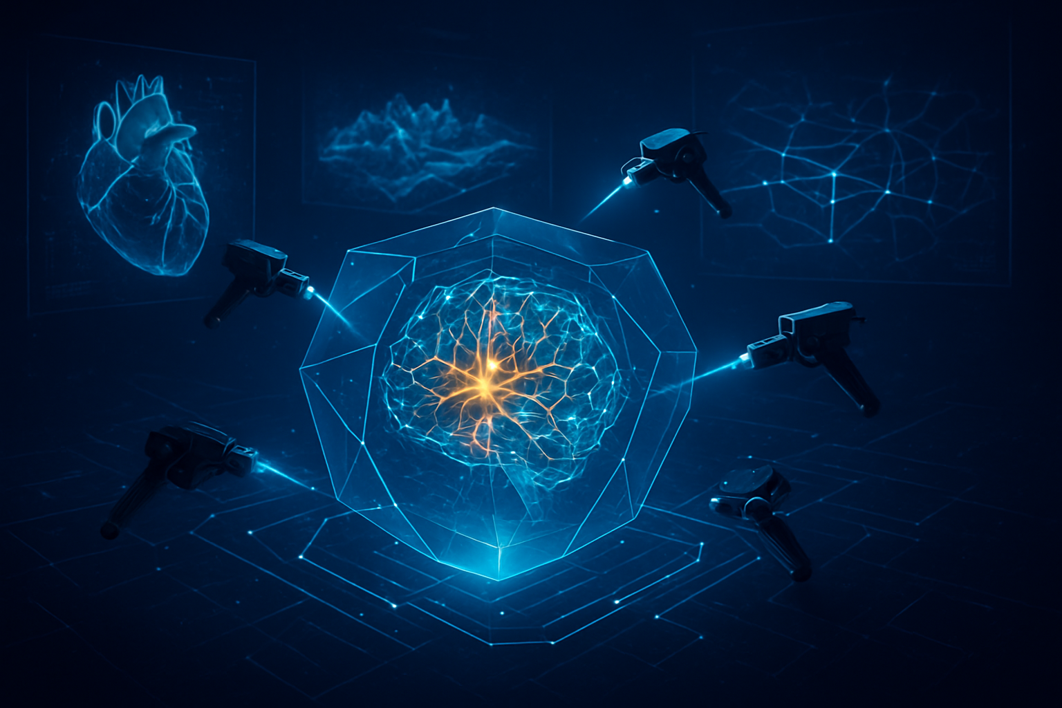
Beyond chip design, the mission introduces "Project Prometheus," a $6.2 billion venture led by Jeff Bezos that works alongside the DOE to apply AI to the physical economy. This includes the use of autonomous laboratories—facilities where AI-driven robotics can conduct experiments 24/7 without human intervention—to discover new superconductors and battery chemistries. These labs, funded by a recent $320 million DOE investment, are expected to shorten the development cycle for energy-dense materials from decades to months. Furthermore, the partnership is deploying AI-enabled digital twins of the national power grid to simulate and manage the massive, fluctuating loads required by next-generation GPU clusters from NVIDIA Corporation (NASDAQ: NVDA).
Initial reactions from the AI research community have been overwhelmingly positive, though some experts note the unprecedented nature of the collaboration. Dr. Aris Constantine, a lead researcher in high-performance computing, noted that "the integration of federal datasets with the agility of commercial cloud providers like Microsoft and Google creates a feedback loop we’ve never seen. We aren't just using AI to find energy; we are using AI to rethink the very physics of how computers consume it."
Industry Impact: The Race for Infrastructure Supremacy
The Genesis Mission fundamentally reshapes the competitive landscape for tech giants and AI labs alike. For the primary cloud partners—Amazon, Google, and Microsoft—the mission provides a direct pipeline to federal research and a regulatory "fast track" for energy infrastructure. By hosting the American Science Cloud (AmSC), these companies solidify their positions as the indispensable backbones of national security and scientific research. This strategic advantage is particularly potent for Microsoft and Google, who are already locked in a fierce battle to integrate AI across every layer of their software and hardware stacks.
The partnership also provides a massive boost to semiconductor manufacturers and specialized AI firms. Companies like NVIDIA Corporation (NASDAQ: NVDA), Advanced Micro Devices, Inc. (NASDAQ: AMD), and Intel Corporation (NASDAQ: INTC) stand to benefit from the DOE’s MEERCAT initiatives, which provide the R&D funding necessary to experiment with high-risk, high-reward chip architectures. Meanwhile, AI labs like OpenAI and Anthropic, who are also signatories to the mission’s MOUs, gain access to a more resilient and scalable energy grid, ensuring their future models aren't throttled by power shortages.
However, the mission may disrupt traditional energy providers. As tech giants increasingly look toward "behind-the-meter" solutions like SMRs and private fusion projects to power their data centers, the reliance on centralized public utilities could diminish. This shift positions companies like Oracle Corporation (NYSE: ORCL), which has recently pivoted toward modular nuclear-powered data centers, as major players in a new "energy-as-a-service" market that bypasses traditional grid limitations.
Broader Significance: AI and the New Energy Paradigm
The Genesis Mission is more than just a technical partnership; it represents a pivot in the global AI race from software optimization to hardware and energy sovereignty. In the broader AI landscape, the initiative signals that the "low-hanging fruit" of large language models has been picked, and the next frontier lies in "embodied AI" and the physical sciences. By aligning AI development with national energy goals, the U.S. is signaling that AI leadership is inseparable from energy leadership.
This development also raises significant questions regarding environmental impact and regulatory oversight. While the mission emphasizes "carbon-free" power through nuclear and fusion, the immediate reality involves a massive buildout of infrastructure that will place immense pressure on local ecosystems and resources. Critics have voiced concerns that the rapid deregulation proposed in the January 2025 Executive Order, "Removing Barriers to American Leadership in Artificial Intelligence," might prioritize speed over safety and environmental standards.
Comparatively, the Genesis Mission is being viewed as the 21st-century equivalent of the Interstate Highway System—a foundational infrastructure project that will enable decades of economic growth. Just as the highway system transformed the American landscape and economy, the Genesis Mission aims to create a "digital-energy highway" that ensures the U.S. remains the global hub for AI innovation, regardless of the energy costs.
Future Horizons: From SMRs to Autonomous Discovery
Looking ahead, the near-term focus of the Genesis Mission will be the deployment of the first AI-optimized Small Modular Reactors. These reactors are expected to be co-located with major data center hubs by 2027, providing a steady, high-capacity power source that is immune to the fluctuations of the broader grid. In the long term, the mission’s "Transformational AI Models Consortium" (ModCon) aims to produce self-improving AI that can autonomously solve the remaining engineering hurdles of commercial fusion energy, potentially providing a "limitless" power source by the mid-2030s.
The applications of this mission extend far beyond energy. The materials discovered in the autonomous labs could revolutionize everything from electric vehicle batteries to aerospace engineering. However, challenges remain, particularly in the realm of cybersecurity. Integrating the DOE’s sensitive datasets with commercial cloud platforms creates a massive attack surface that will require the development of new, AI-driven "zero-trust" security protocols. Experts predict that the next year will see a surge in public-private "red-teaming" exercises to ensure the Genesis Mission’s infrastructure remains secure from foreign interference.
A New Chapter in AI History
The Genesis Mission marks a definitive shift in how the world approaches the AI revolution. By acknowledging that the future of intelligence is inextricably linked to the future of energy, the U.S. Department of Energy and its partners in the private sector have laid the groundwork for a sustainable, high-growth AI economy. The mission successfully bridges the gap between theoretical research and industrial application, ensuring that the "Big Three"—Amazon, Google, and Microsoft—along with semiconductor leaders like NVIDIA, have the resources needed to push the boundaries of what is possible.
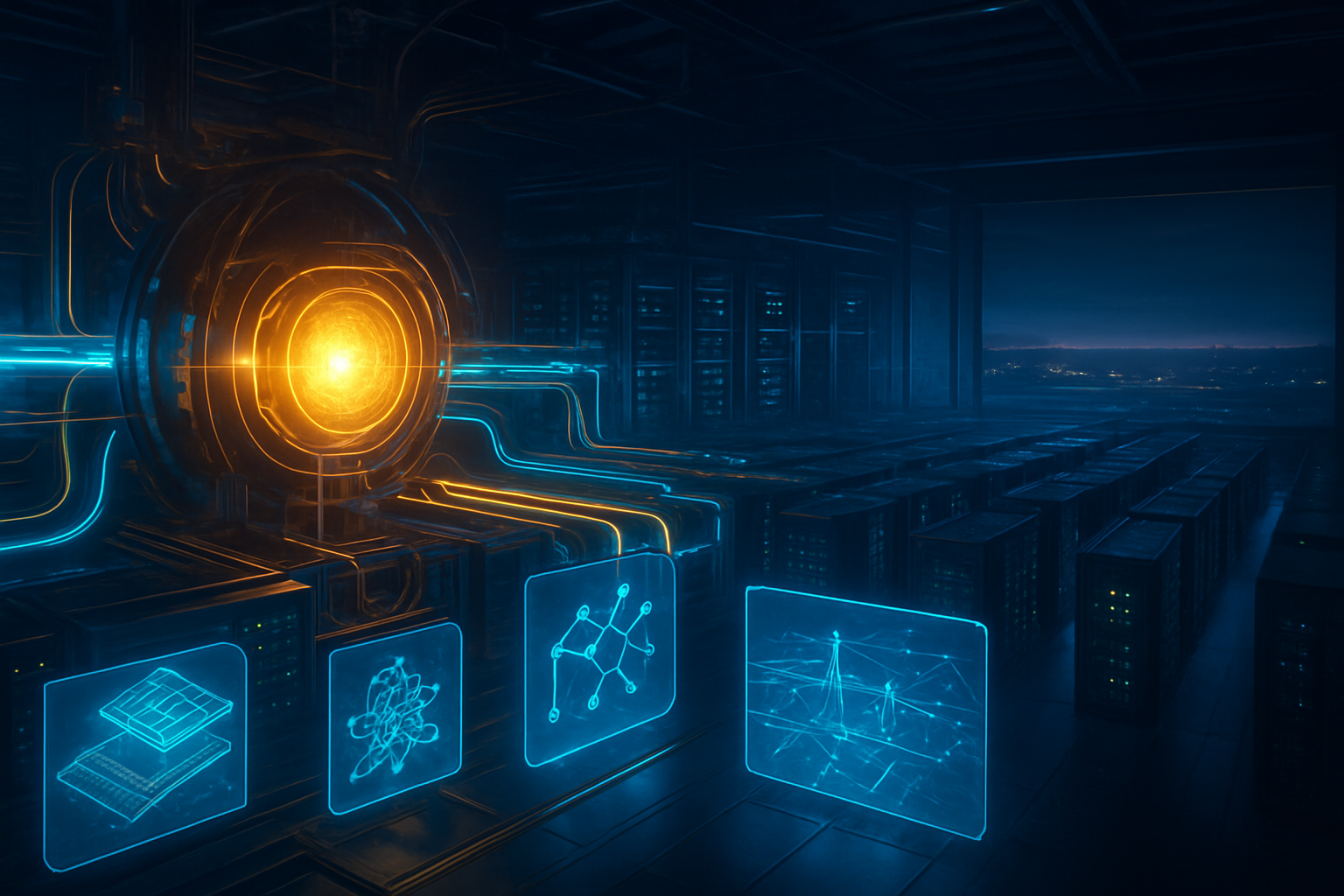
As we move into 2026, the success of the Genesis Mission will be measured not just by the benchmarks of AI models, but by the stability of the power grid and the speed of material discovery. This initiative is a bold bet on the idea that AI can solve the very problems it creates, using its immense processing power to unlock the clean, abundant energy required for its own evolution. The coming months will be crucial as the first $320 million in funding is deployed and the "American Science Cloud" begins its initial operations, marking the start of a new era in the synergy between man, machine, and the atom.
This content is intended for informational purposes only and represents analysis of current AI developments.
TokenRing AI delivers enterprise-grade solutions for multi-agent AI workflow orchestration, AI-powered development tools, and seamless remote collaboration platforms.
For more information, visit https://www.tokenring.ai/.