In a breakthrough that many are calling the "Penicillin Moment" of the 21st century, researchers at the Massachusetts Institute of Technology, led by bioengineering pioneer James Collins, have successfully leveraged generative AI to discover an entirely new class of antibiotics capable of neutralizing the deadly, drug-resistant superbug MRSA. This development, which reached a critical clinical milestone in February 2026, marks the first time that generative AI has not just helped find a drug, but has autonomously designed a molecular structure that bacteria have no natural defense against.
The discovery’s significance cannot be overstated. For decades, the pharmaceutical industry has been locked in an "arms race" it was losing, with traditional drug discovery taking upwards of ten years and billions of dollars to bring a single antibiotic to market. By using a "lab-in-the-loop" system that integrates generative AI with robotic synthesis, the MIT team has slashed that timeline from years to just months. With MRSA (Methicillin-resistant Staphylococcus aureus) claiming over 100,000 lives annually worldwide, this AI-driven acceleration represents a fundamental shift from reactive medicine to proactive, algorithmic defense.
The Architecture of Discovery: Beyond the 'Black Box'
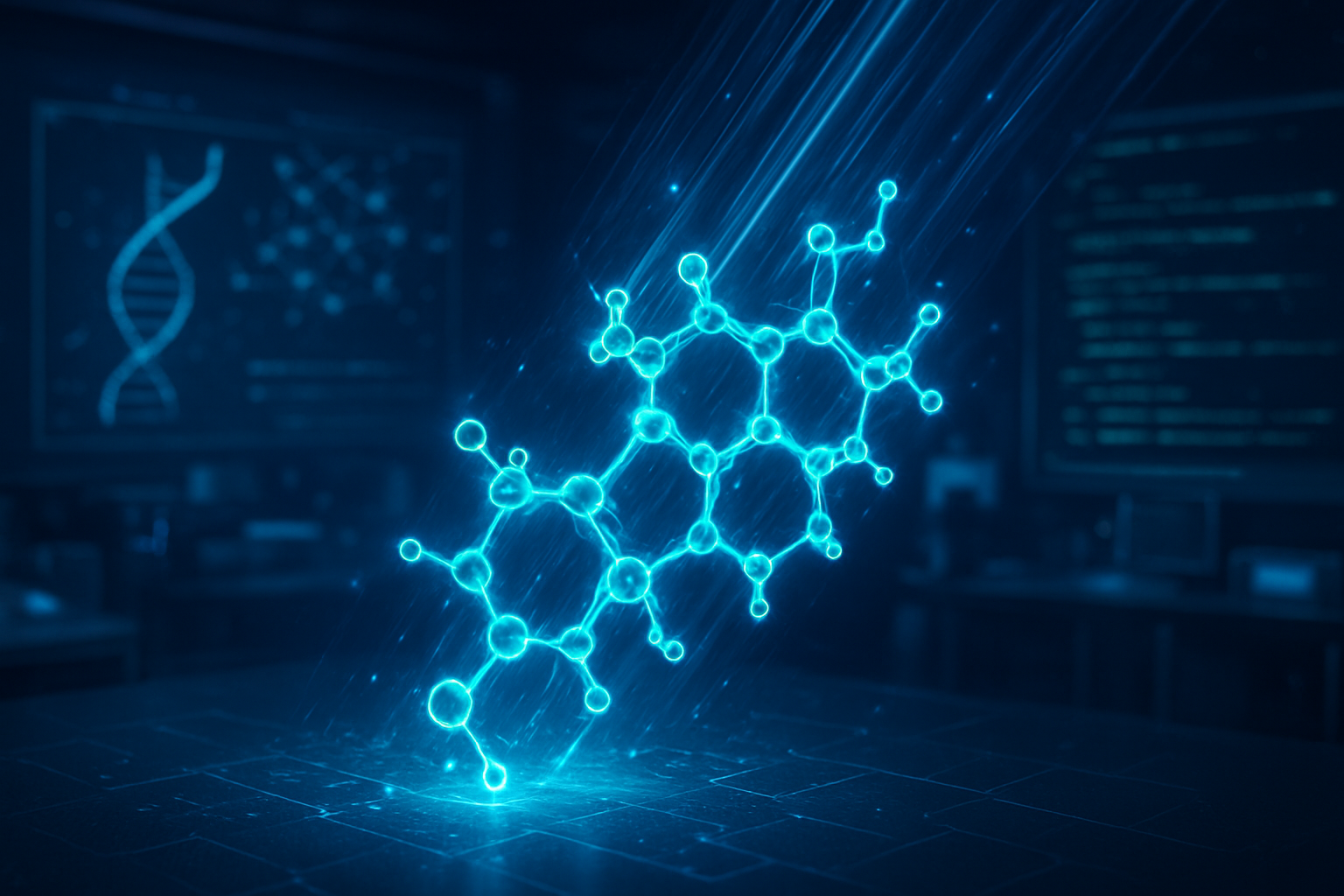
The technical foundation of this breakthrough lies in a shift from "predictive" to "generative" deep learning. In late 2023, Collins' team utilized Graph Neural Networks (GNNs) to screen millions of existing compounds—a process that led to the discovery of Halicin. However, the 2025-2026 breakthroughs moved into the realm of de novo design. Using Variational Autoencoders (VAEs) and diffusion-based models, the researchers didn't just search through a digital library; they asked the AI to "write" the chemical code for a molecule that was lethal to MRSA but harmless to human cells.
This approach utilizes what researchers call "explainable AI." Unlike previous models that operated as "black boxes," the MIT system was designed to identify which specific chemical substructures were responsible for antibiotic potency. By understanding the "grammar" of these molecules, the AI could perform multi-objective optimization—solving for efficacy, toxicity, and metabolic stability simultaneously. In the case of the lead candidate, dubbed DN1, the AI evaluated over 36 million hypothetical compounds in silico, narrowing them down to just 24 candidates for physical synthesis. This represents a 99.9% reduction in the physical "hit-to-lead" workload compared to traditional medicinal chemistry.
Initial reactions from the AI research community have been electric. "We are no longer limited by what nature has provided or what humans can imagine," says Dr. Sarah Jenkins, an AI researcher not involved in the study. "The MIT team has demonstrated that AI can navigate the 'dark' chemical space—the trillions of possible molecular combinations that have never existed on Earth—to find the exact key for a bacterial lock."
The TechBio Explosion: Market Leaders and Strategic Shifts
The success of the Collins lab has sent shockwaves through the pharmaceutical and technology sectors, accelerating the rise of "TechBio" firms. Public companies that pioneered AI drug discovery are seeing a massive surge in strategic relevance. Recursion Pharmaceuticals (NASDAQ: RXRX) and Absci Corp (NASDAQ: ABSI) have both announced expansions to their generative platforms in early 2026, aiming to replicate the "Collins Method" for oncology and autoimmune diseases. Meanwhile, Schrödinger, Inc. (NASDAQ: SDGR) has integrated similar generative "physics-informed" AI into its LiveDesign software, which is now a staple in Big Pharma labs.
The competitive landscape is also shifting toward the infrastructure providers who power these models. NVIDIA (NASDAQ: NVDA), which recently launched its BioNeMo "agentic" AI platform, has become the de facto operating system for these high-speed labs. By providing the compute power necessary to simulate 36 million molecular interactions in days rather than years, NVIDIA has solidified its position as a central player in the future of healthcare. Major pharmaceutical giants like Roche (OTC: RHHBY) and Eli Lilly (NYSE: LLY) are no longer just licensing drugs; they are aggressively acquiring AI startups to bring these generative capabilities in-house, fearing that those without "lab-in-the-loop" automation will be priced out of the market by the end of the decade.
A New Era of Biosecurity and Ethical Challenges
While the discovery of DN1 is a triumph, it has also sparked a necessary debate about the broader AI landscape. The ability of AI to design "perfect" antibiotics also implies a "dual-use" risk: the same models could, in theory, be "flipped" to design novel toxins or nerve agents. In response, the FDA and international regulatory bodies have implemented the "Good AI Practice (GAIP)" principles as of January 2026. These regulations require drug sponsors to provide a "traceability audit" of the AI models used, ensuring that the path from digital design to physical drug is transparent and secure.
Furthermore, some evolutionary biologists warn of "AI-designed resistance." While the MIT team’s AI focuses on mechanisms that are difficult for bacteria to evolve around—such as disrupting the proton motive force of the cell membrane—the sheer speed of AI discovery could outpace our ability to monitor long-term ecological impacts. Despite these concerns, the impact of this breakthrough is being compared to the 2020 arrival of AlphaFold. Just as AlphaFold solved the protein-folding problem, the MIT MRSA discovery is being hailed as the solution to the "antibiotic drought," proving that AI can solve biological challenges that have stumped human scientists for over half a century.
The Horizon: Agentic Labs and Universal Antibiotics
Looking ahead, the near-term focus is on the clinical transition. Phare Bio, the non-profit venture co-founded by Collins, is currently moving DN1 and another lead candidate for gonorrhea, NG1, toward human clinical trials with support from a massive ARPA-H grant. Experts predict that the next two years will see the emergence of "Agentic AI Labs," where AI "scientists" autonomously propose, execute, and analyze experiments in robotic "wet labs" with minimal human intervention.
The long-term goal is the creation of a "universal antibiotic designer"—an AI system that can be deployed the moment a new pathogen emerges, designing a targeted cure in weeks. Challenges remain, particularly in the realm of long-term toxicity and the "interpretability" of complex AI designs, but the momentum is undeniable. "The bottleneck in drug discovery is no longer our imagination or our ability to screen," James Collins noted in a recent symposium. "The bottleneck is now only the speed at which we can safely conduct clinical trials."
Closing Thoughts: A Landmark in Human History
The discovery of AI-designed MRSA antibiotics will likely be remembered as the moment the pharmaceutical industry finally broke free from the constraints of 20th-century trial-and-error chemistry. By compressing a five-year discovery process into a single season, James Collins and his team have not only provided a potential cure for a deadly superbug but have also provided a blueprint for the future of all medicine.
As we move through the early months of 2026, the focus will shift from the laboratory to the clinic. Watch for the first Phase I trial results of DN1, as well as new regulatory frameworks from the FDA regarding the "credibility" of AI-generated molecular data. We are entering an era where the "code" for a cure can be written as easily as a line of software—a development that promises to save millions of lives in the decades to come.
This content is intended for informational purposes only and represents analysis of current AI developments.
TokenRing AI delivers enterprise-grade solutions for multi-agent AI workflow orchestration, AI-powered development tools, and seamless remote collaboration platforms.
For more information, visit https://www.tokenring.ai/.