Elon Musk's artificial intelligence startup, xAI, is reportedly pursuing an monumental $20 billion deal to lease Nvidia (NASDAQ: NVDA) chips, a move that dramatically reshapes the landscape of AI infrastructure and intensifies the global race for computational supremacy. This colossal agreement, which began to surface in media reports around October 7-8, 2025, and continued through October 16, 2025, highlights the escalating demand for high-performance computing power within the AI industry and xAI's audacious ambitions.
The proposed $20 billion deal involves a unique blend of equity and debt financing, orchestrated through a "special purpose vehicle" (SPV). This innovative SPV is tasked with directly acquiring Nvidia (NASDAQ: NVDA) Graphics Processing Units (GPUs) and subsequently leasing them to xAI for a five-year term. Notably, Nvidia itself is slated to contribute up to $2 billion to the equity portion of this financing, cementing its strategic partnership. The chips are specifically earmarked for xAI's "Colossus 2" data center project in Memphis, Tennessee, which is rapidly becoming the company's largest facility to date, with plans to potentially double its GPU count to 200,000 and eventually scale to millions. This unprecedented financial maneuver is a clear signal of xAI's intent to become a dominant force in the generative AI space, challenging established giants and setting new benchmarks for infrastructure investment.
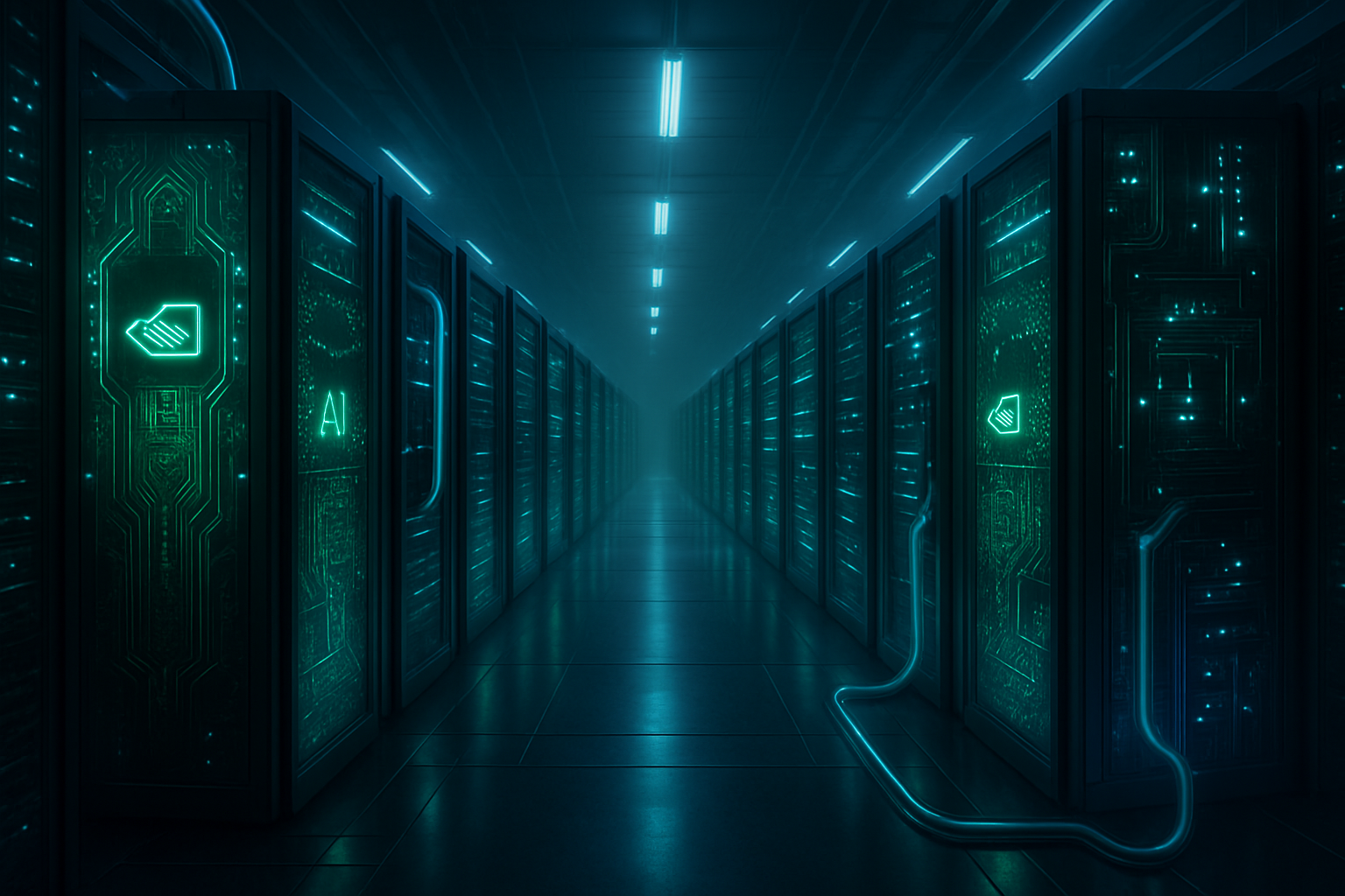
Unpacking the Technical Blueprint: xAI's Gigawatt-Scale Ambition
The xAI-Nvidia (NASDAQ: NVDA) deal is not merely a financial transaction; it's a technical gambit designed to secure an unparalleled computational advantage. The $20 billion package, reportedly split into approximately $7.5 billion in new equity and up to $12.5 billion in debt, is funneled through an SPV, which will directly purchase Nvidia's advanced GPUs. This debt is uniquely secured by the GPUs themselves, rather than xAI's corporate assets, a novel approach that has garnered both admiration and scrutiny from financial experts. Nvidia's direct equity contribution further intertwines its fortunes with xAI, solidifying its role as both a critical supplier and a strategic partner.
xAI's infrastructure strategy for its "Colossus 2" data center in Memphis, Tennessee, represents a significant departure from traditional AI development. The initial "Colossus 1" site already boasts over 200,000 Nvidia H100 GPUs. For "Colossus 2," the focus is shifting to even more advanced hardware, with plans for 550,000 Nvidia GB200 and GB300 GPUs, aiming for an eventual total of 1 million GPUs within the entire Colossus ecosystem. Elon Musk has publicly stated an audacious goal for xAI to deploy 50 million "H100 equivalent" AI GPUs within the next five years. This scale is unprecedented, requiring a "gigawatt-scale" facility – one of the largest, if not the largest, AI-focused data centers globally, with xAI constructing its own dedicated power plant, Stateline Power, in Mississippi, to supply over 1 gigawatt by 2027.
This infrastructure strategy diverges sharply from many competitors, such as OpenAI and Anthropic, who heavily rely on cloud partnerships. xAI's "vertical integration play" aims for direct ownership and control over its computational resources, mirroring Musk's successful strategies with Tesla (NASDAQ: TSLA) and SpaceX. The rapid deployment speed of Colossus, with Colossus 1 brought online in just 122 days, sets a new industry standard. Initial reactions from the AI community are a mix of awe at the financial innovation and scale, and concern over the potential for market concentration and the immense energy demands. Some analysts view the hardware-backed debt as "financial engineering theater," while others see it as a clever blueprint for future AI infrastructure funding.
Competitive Tremors: Reshaping the AI Industry Landscape
The xAI-Nvidia (NASDAQ: NVDA) deal is a seismic event in the AI industry, intensifying the already fierce "AI arms race" and creating significant competitive implications for all players.
xAI stands to be the most immediate beneficiary, gaining access to an enormous reservoir of computational power. This infrastructure is crucial for its "Colossus 2" data center project, accelerating the development of its AI models, including the Grok chatbot, and positioning xAI as a formidable challenger to established AI labs like OpenAI and Alphabet's (NASDAQ: GOOGL) Google DeepMind. The lease structure also offers a critical lifeline, mitigating some of the direct financial risk associated with such large-scale hardware acquisition.
Nvidia further solidifies its "undisputed leadership" in the AI chip market. By investing equity and simultaneously supplying hardware, Nvidia employs a "circular financing model" that effectively finances its own sales and embeds it deeper into the foundational AI infrastructure. This strategic partnership ensures substantial long-term demand for its high-end GPUs and enhances Nvidia's brand visibility across Elon Musk's broader ecosystem, including Tesla (NASDAQ: TSLA) and X (formerly Twitter). The $2 billion investment is a low-risk move for Nvidia, representing a minor fraction of its revenue while guaranteeing future demand.
For other major AI labs and tech companies, this deal intensifies pressure. While companies like OpenAI (in partnership with Microsoft (NASDAQ: MSFT)), Meta Platforms (NASDAQ: META), and Oracle (NYSE: ORCL) have also made multi-billion dollar commitments to AI infrastructure, xAI's direct ownership model and the sheer scale of its planned GPU deployment could further tighten the supply of high-end Nvidia GPUs. This necessitates greater investment in proprietary hardware or more aggressive long-term supply agreements for others to remain competitive. The deal also highlights a potential disruption to existing cloud computing models, as xAI's strategy of direct data center ownership contrasts with the heavy cloud reliance of many competitors. This could prompt other large AI players to reconsider their dependency on major cloud providers for core AI training infrastructure.
Broader Implications: The AI Landscape and Looming Concerns
The xAI-Nvidia (NASDAQ: NVDA) deal is a powerful indicator of several overarching trends in the broader AI landscape, while simultaneously raising significant concerns.
Firstly, it underscores the escalating AI compute arms race, where access to vast computational power is now the primary determinant of competitive advantage in developing frontier AI models. This deal, along with others from OpenAI, Meta Platforms (NASDAQ: META), and Oracle (NYSE: ORCL), signifies that the "most expensive corporate battle of the 21st century" is fundamentally a race for hardware. This intensifies GPU scarcity and further solidifies Nvidia's near-monopoly in AI hardware, as its direct investment in xAI highlights its strategic role in accelerating customer AI development.
However, this massive investment also amplifies potential concerns. The most pressing is energy consumption. Training and operating AI models at the scale xAI envisions for "Colossus 2" will demand enormous amounts of electricity, primarily from fossil fuels, contributing significantly to greenhouse gas emissions. AI data centers are expected to account for a substantial portion of global energy demand by 2030, straining power grids and requiring advanced cooling systems that consume millions of gallons of water annually. xAI's plans for a dedicated power plant and wastewater processing facility in Memphis acknowledge these challenges but also highlight the immense environmental footprint of frontier AI.
Another critical concern is the concentration of power. The astronomical cost of compute resources leads to a "de-democratization of AI," concentrating development capabilities in the hands of a few well-funded entities. This can stifle innovation from smaller startups, academic institutions, and open-source initiatives, limiting the diversity of ideas and applications. The innovative "circular financing" model, while enabling xAI's rapid scaling, also raises questions about financial transparency and the potential for inflating reported capital raises without corresponding organic revenue growth, reminiscent of past tech bubbles.
Compared to previous AI milestones, this deal isn't a singular algorithmic breakthrough like AlphaGo but rather an evolutionary leap in infrastructure scaling. It is a direct consequence of the "more compute leads to better models" paradigm established by the emergence of Large Language Models (LLMs) like GPT-3 and GPT-4. The xAI-Nvidia deal, much like Microsoft's (NASDAQ: MSFT) investment in OpenAI or the "Stargate" project by OpenAI and Oracle (NYSE: ORCL), signifies that the current phase of AI development is defined by building "AI factories"—massive, dedicated data centers designed for AI training and deployment.
The Road Ahead: Anticipating Future AI Developments
The xAI-Nvidia (NASDAQ: NVDA) chips lease deal sets the stage for a series of transformative developments, both in the near and long term, for xAI and the broader AI industry.
In the near term (next 1-2 years), xAI is aggressively pursuing the construction and operationalization of its "Colossus 2" data center in Memphis, aiming to establish the world's most powerful AI training cluster. Following the deployment of 200,000 H100 GPUs, the immediate goal is to reach 1 million GPUs by December 2025. This rapid expansion will fuel the evolution of xAI's Grok models. Grok 3, unveiled in February 2025, significantly boosted computational power and introduced features like "DeepSearch" and "Big Brain Mode," excelling in reasoning and multimodality. Grok 4, released in July 2025, further advanced multimodal processing and real-time data integration with Elon Musk's broader ecosystem, including X (formerly Twitter) and Tesla (NASDAQ: TSLA). Grok 5 is slated for a September 2025 unveiling, with aspirations for AGI-adjacent capabilities.
Long-term (2-5+ years), xAI intends to scale its GPU cluster to 2 million by December 2026 and an astonishing 3 million GPUs by December 2027, anticipating the use of next-generation Nvidia chips like Rubins or Ultrarubins. This hardware-backed financing model could become a blueprint for future infrastructure funding. Potential applications for xAI's advanced models extend across software development, research, education, real-time information processing, and creative and business solutions, including advanced AI agents and "world models" capable of simulating real-world environments.
However, this ambitious scaling faces significant challenges. Power consumption is paramount; the projected 3 million GPUs by 2027 could require nearly 5,000 MW, necessitating dedicated private power plants and substantial grid upgrades. Cooling is another hurdle, as high-density GPUs generate immense heat, demanding liquid cooling solutions and consuming vast amounts of water. Talent acquisition for specialized AI infrastructure, including thermal engineers and power systems architects, will be critical. The global semiconductor supply chain remains vulnerable, and the rapid evolution of AI models creates a "moving target" for hardware designers.
Experts predict an era of continuous innovation and fierce competition. The AI chip market is projected to reach $1.3 trillion by 2030, driven by specialization. Physical AI infrastructure is increasingly seen as an insurmountable strategic advantage. The energy crunch will intensify, making power generation a national security imperative. While AI will become more ubiquitous through NPUs in consumer devices and autonomous agents, funding models may pivot towards sustainability over "growth-at-all-costs," and new business models like conversational commerce and AI-as-a-service will emerge.
A New Frontier: Assessing AI's Trajectory
The $20 billion Nvidia (NASDAQ: NVDA) chips lease deal by xAI is a landmark event in the ongoing saga of artificial intelligence, serving as a powerful testament to both the immense capital requirements for cutting-edge AI development and the ingenious financial strategies emerging to meet these demands. This complex agreement, centered on xAI securing a vast quantity of advanced GPUs for its "Colossus 2" data center, utilizes a novel, hardware-backed financing structure that could redefine how future AI infrastructure is funded.
The key takeaways underscore the deal's innovative nature, with an SPV securing debt against the GPUs themselves, and Nvidia's strategic role as both a supplier and a significant equity investor. This "circular financing model" not only guarantees demand for Nvidia's high-end chips but also deeply intertwines its success with that of xAI. For xAI, the deal is a direct pathway to achieving its ambitious goal of directly owning and operating gigawatt-scale data centers, a strategic departure from cloud-reliant competitors, positioning it to compete fiercely in the generative AI race.
In AI history, this development signifies a new phase where the sheer scale of compute infrastructure is as critical as algorithmic breakthroughs. It pioneers a financing model that, if successful, could become a blueprint for other capital-intensive tech ventures, potentially democratizing access to high-end GPUs while also highlighting the immense financial risks involved. The deal further cements Nvidia's unparalleled dominance in the AI chip market, creating a formidable ecosystem that will be challenging for competitors to penetrate.
The long-term impact could see the xAI-Nvidia model shape future AI infrastructure funding, accelerating innovation but also potentially intensifying industry consolidation as smaller players struggle to keep pace with the escalating costs. It will undoubtedly lead to increased scrutiny on the economics and sustainability of the AI boom, particularly concerning high burn rates and complex financial structures.
In the coming weeks and months, observers should closely watch the execution and scaling of xAI's "Colossus 2" data center in Memphis. The ultimate validation of this massive investment will be the performance and capabilities of xAI's next-generation AI models, particularly the evolution of Grok. Furthermore, the industry will be keen to see if this SPV-based, hardware-collateralized financing model is replicated by other AI companies or hardware vendors. Nvidia's financial reports and any regulatory commentary on these novel structures will also provide crucial insights into the evolving landscape of AI finance. Finally, the progress of xAI's associated power infrastructure projects, such as the Stateline Power plant, will be vital, as energy supply emerges as a critical bottleneck for large-scale AI.
This content is intended for informational purposes only and represents analysis of current AI developments.
TokenRing AI delivers enterprise-grade solutions for multi-agent AI workflow orchestration, AI-powered development tools, and seamless remote collaboration platforms.
For more information, visit https://www.tokenring.ai/.