Author: mdierolf

  • Walmart and OpenAI Forge Groundbreaking Alliance for AI-Driven Shopping via ChatGPT

    Walmart and OpenAI Forge Groundbreaking Alliance for AI-Driven Shopping via ChatGPT

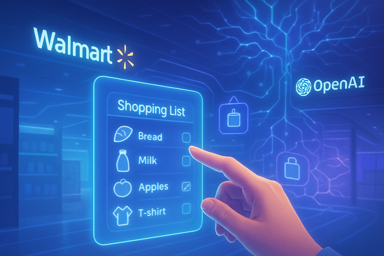
    In a landmark announcement that sent ripples across the retail and technology sectors yesterday, October 14, 2025, retail behemoth Walmart (NYSE: WMT) officially unveiled a strategic partnership with artificial intelligence pioneer OpenAI. This collaboration is set to revolutionize the online shopping experience by integrating advanced AI capabilities directly into ChatGPT, allowing customers to engage in "agentic commerce" through conversational interfaces. The move signals a significant leap in how consumers will interact with e-commerce platforms, promising a future where shopping is not just personalized but proactively intelligent.

    This unprecedented alliance aims to transform the transactional nature of online retail into a seamless, intuitive, and highly personalized dialogue. By leveraging OpenAI's cutting-edge language models and newly introduced "Instant Checkout" feature, Walmart is positioning itself at the forefront of AI-powered commerce, redefining convenience and efficiency for its vast customer base and loyalty members across Walmart and Sam's Club. The immediate significance lies in the potential for mass adoption of truly conversational shopping, moving beyond the traditional search bar and into a dynamic, AI-guided purchasing journey.

    The Dawn of Agentic Commerce: A Technical Deep Dive into Conversational Retail

    The core of the Walmart-OpenAI partnership lies in its innovative approach to AI-driven shopping, fundamentally shifting from reactive search to proactive, "agentic commerce." At its heart, customers will be able to "Chat and Buy" directly within ChatGPT using natural language, either through text or voice commands. This goes far beyond simple product searches; the system is designed to understand complex requests and anticipate user needs. For instance, a user planning a "Taco Tuesday" dinner can simply ask ChatGPT to find all necessary ingredients, and the AI will curate a comprehensive grocery list, ready for purchase.

    Technically, this experience is powered by OpenAI's recently launched "Instant Checkout" feature, which enables direct purchases within the ChatGPT interface. This feature, initially rolled out for Etsy sellers and slated for Shopify (NYSE: SHOP) merchants, facilitates a frictionless transaction process, eliminating the need for users to navigate to external websites or applications. The underlying mechanism, dubbed "Agentic Commerce Protocol," was co-developed by OpenAI and Stripe (NYSE: STRIP), ensuring secure and efficient payment processing. Initially, the Instant Checkout system will support single-item purchases, with ambitious plans to expand to multi-item carts and additional geographical regions, signifying a phased but rapid deployment strategy.

    This approach dramatically differs from previous e-commerce models, which predominantly relied on keyword searches, curated product listings, and manual navigation. While some retailers have experimented with AI chatbots, their functionalities have largely been limited to customer service or basic product recommendations. The Walmart-OpenAI integration, however, introduces a truly multi-media, personalized, and contextual shopping experience. It's an AI that learns, plans, and predicts, effectively acting as a personal shopping assistant that evolves with the consumer's habits and preferences. Initial reactions from the AI research community and industry experts highlight this as a pivotal moment, demonstrating the practical application of large language models (LLMs) in transforming real-world consumer interactions at an unprecedented scale.

    Reshaping the Retail Landscape: Implications for AI Companies and Tech Giants

    This groundbreaking partnership between Walmart (NYSE: WMT) and OpenAI sends a clear signal to the entire tech and retail industry: AI is no longer just a backend optimization tool but a front-facing, revenue-generating engine. Walmart stands to benefit immensely, solidifying its position as an innovator in digital retail and potentially capturing a significant share of the burgeoning conversational commerce market. By being an early mover in integrating advanced LLMs into its core shopping experience, Walmart gains a strategic advantage over competitors, particularly Amazon (NASDAQ: AMZN), which has traditionally dominated online retail. While Amazon has its own AI capabilities (like Alexa), the direct, conversational "Chat and Buy" integration within a widely adopted platform like ChatGPT represents a novel and potentially more fluid user experience.

    For OpenAI, this collaboration is a massive validation of its generative AI capabilities and its strategic push into "agentic commerce." The partnership with a retail giant like Walmart demonstrates the commercial viability and scalability of its Instant Checkout and Agentic Commerce Protocol. This move positions OpenAI not just as a developer of foundational AI models but as a critical enabler of next-generation digital marketplaces. Other AI labs and tech companies will undoubtedly feel the pressure to innovate in similar conversational commerce spaces. Companies like Google (NASDAQ: GOOGL), Meta (NASDAQ: META), and Apple (NASDAQ: AAPL), all with significant AI investments and consumer-facing platforms, will likely accelerate their efforts to integrate sophisticated shopping functionalities into their own AI assistants and ecosystems to avoid being left behind.

    The potential disruption to existing products and services is substantial. Traditional e-commerce interfaces, comparison shopping sites, and even some niche shopping apps could face significant challenges as consumers gravitate towards the ease and intelligence of AI-driven conversational shopping. Market positioning will increasingly depend on the seamless integration of AI into the customer journey, with companies that can offer personalized, predictive, and frictionless experiences gaining a significant competitive edge. This partnership underscores a strategic shift where AI companies are becoming direct partners in consumer transactions, rather than just providing underlying technology, thereby reshaping the competitive dynamics across both the AI and retail sectors.

    The Broader AI Landscape: A Paradigm Shift in Consumer Interaction

    The Walmart-OpenAI partnership represents more than just a new feature; it signifies a profound shift in the broader AI landscape, particularly in how artificial intelligence is expected to interact with and serve consumers. This move towards "agentic commerce" aligns perfectly with the overarching trend of AI becoming more proactive and less reactive. Instead of merely responding to explicit commands, AI is now being designed to anticipate needs, plan complex tasks (like meal planning), and execute multi-step processes (like shopping and checkout) autonomously. This is a significant evolution from earlier AI applications, which were often siloed or offered limited interactive capabilities.

    The impacts are far-reaching. For consumers, it promises unparalleled convenience and personalization, potentially reducing decision fatigue and saving time. Imagine an AI that not only knows your dietary preferences but also your typical shopping list, prompting you to restock essentials before you even realize you're running low. However, this level of integration also raises potential concerns, particularly around data privacy and security. The linking of personal shopping habits and financial information to an AI platform necessitates robust safeguards and transparent data handling policies. There's also the question of algorithmic bias in product recommendations and the potential for over-reliance on AI for purchasing decisions, which could impact consumer autonomy.

    Comparing this to previous AI milestones, the Walmart-OpenAI collaboration stands out as a major step in the commercialization and mainstream adoption of advanced generative AI. While the introduction of voice assistants like Alexa and Google Assistant marked an initial foray into conversational AI, their shopping capabilities remained relatively rudimentary. This new partnership, leveraging the sophisticated understanding and generation capabilities of ChatGPT, pushes the boundaries into truly intelligent and transactional conversations. It echoes the transformative impact of early e-commerce platforms but with an added layer of AI-driven intelligence that fundamentally alters the user experience, moving from browsing to a guided, predictive interaction.

    Future Horizons: What's Next for AI-Driven Retail

    Looking ahead, the Walmart-OpenAI partnership is merely the beginning of a transformative era for AI-driven retail. In the near-term, we can expect the gradual rollout of the "Chat and Buy" feature to Walmart (NYSE: WMT) and Sam's Club customers across the US, initially focusing on single-item purchases. The expansion to multi-item carts and more complex shopping scenarios, such as subscription management and personalized recommendations based on evolving lifestyle needs, is a highly anticipated next step. Beyond basic transactions, the "Agentic Commerce Protocol" could evolve to integrate with smart home devices, automatically reordering groceries when stock is low, or suggesting recipes based on available ingredients and dietary goals.

    Long-term developments are poised to see AI becoming an indispensable personal shopping agent that understands not just what you want to buy, but why, when, and how you prefer to shop. This could lead to a hyper-personalized retail experience where AI anticipates needs even before they manifest, offering curated selections, exclusive deals, and proactive problem-solving. Potential applications extend beyond groceries to fashion, electronics, and even services, with AI assisting in booking appointments or managing subscriptions based on user preferences and schedules.

    However, several challenges need to be addressed for this vision to fully materialize. Ensuring the ethical use of AI, particularly concerning data privacy and algorithmic transparency, will be paramount. Developing robust security measures to protect sensitive customer data and financial information is crucial. Furthermore, refining the AI's understanding of nuanced human language and intent, especially in complex or ambiguous shopping scenarios, will require continuous development. Experts predict that the success of this model will spur other major retailers and tech companies to invest heavily in similar "agentic" AI solutions, leading to a highly competitive landscape where the most intelligent and trustworthy AI assistants will gain consumer loyalty. The evolution of the "Instant Checkout" feature to support a wider array of merchants and product categories will also be a key indicator of its broader market impact.

    The AI Retail Revolution: A Concluding Assessment

    The recent announcement of the partnership between Walmart (NYSE: WMT) and OpenAI to launch AI-driven shopping through ChatGPT marks a pivotal moment in the history of both artificial intelligence and retail. The key takeaway is the shift towards "agentic commerce," where AI moves beyond simple chatbots to become a proactive, intelligent assistant capable of understanding complex needs, planning purchases, and executing transactions directly within a conversational interface. This integration of OpenAI's advanced language models and "Instant Checkout" feature into Walmart's vast retail ecosystem is set to redefine consumer expectations for convenience, personalization, and efficiency in online shopping.

    This development holds immense significance in AI history, illustrating the maturation of large language models from experimental tools to commercially viable engines driving fundamental changes in consumer behavior. It underscores the accelerating trend of AI becoming deeply embedded in our daily lives, transforming mundane tasks into seamless, intelligent interactions. While offering unprecedented convenience, it also brings to the forefront critical discussions around data privacy, algorithmic ethics, and the evolving relationship between humans and AI in commercial contexts.

    In the long term, this partnership is likely to be remembered as a catalyst that spurred a new wave of innovation in conversational commerce. It sets a new benchmark for how retailers and technology companies will collaborate to leverage AI for enhanced customer experiences. What to watch for in the coming weeks and months includes the initial rollout and customer adoption rates of the "Chat and Buy" feature, the expansion of "Instant Checkout" to multi-item carts and other merchants, and how competitors will respond to this bold strategic move. The AI retail revolution has truly begun, and its trajectory will be shaped by how effectively these intelligent systems can deliver on their promise while navigating the inherent challenges of advanced AI integration.


    This content is intended for informational purposes only and represents analysis of current AI developments.

    TokenRing AI delivers enterprise-grade solutions for multi-agent AI workflow orchestration, AI-powered development tools, and seamless remote collaboration platforms.
    For more information, visit https://www.tokenring.ai/.

  • NVIDIA Fuels Starship Dreams: Jensen Huang Delivers Petaflop AI Supercomputer to SpaceX

    NVIDIA Fuels Starship Dreams: Jensen Huang Delivers Petaflop AI Supercomputer to SpaceX

    October 15, 2025 – In a move poised to redefine the intersection of artificial intelligence and space exploration, NVIDIA (NASDAQ: NVDA) CEO Jensen Huang personally delivered a cutting-edge 128GB AI supercomputer, the DGX Spark, to Elon Musk at SpaceX's Starbase facility. This pivotal moment, occurring amidst the advanced preparations for Starship's rigorous testing, signifies a strategic leap towards embedding powerful, localized AI capabilities directly into the heart of space technology development. The partnership between the AI hardware giant and the ambitious aerospace innovator is set to accelerate breakthroughs in autonomous spaceflight, real-time data analysis, and the overall efficiency of next-generation rockets, pushing the boundaries of what's possible for humanity's multi-planetary future.

    The immediate significance of this delivery lies in providing SpaceX with unprecedented on-site AI computing power. The DGX Spark, touted as the world's smallest AI supercomputer, packs a staggering petaflop of AI performance and 128GB of unified memory into a compact, desktop-sized form factor. This allows SpaceX engineers to prototype, fine-tune, and run inference for complex AI models with up to 200 billion parameters locally, bypassing the latency and costs associated with constant cloud interaction. For Starship's rapid development and testing cycles, this translates into accelerated analysis of vast flight data, enhanced autonomous system refinement for flight control and landing, and a truly portable supercomputing capability essential for a dynamic testing environment.

    Unpacking the Petaflop Powerhouse: The DGX Spark's Technical Edge

    The NVIDIA DGX Spark is an engineering marvel, designed to democratize access to petaflop-scale AI performance. At its core lies the NVIDIA GB10 Grace Blackwell Superchip, which seamlessly integrates a powerful Blackwell GPU with a 20-core Arm-based Grace CPU. This unified architecture delivers an astounding one petaflop of AI performance at FP4 precision, coupled with 128GB of LPDDR5X unified CPU-GPU memory. This shared memory space is crucial, as it eliminates data transfer bottlenecks common in systems with separate memory pools, allowing for the efficient processing of incredibly large and complex AI models.

    Capable of running inference on AI models up to 200 billion parameters and fine-tuning models up to 70 billion parameters locally, the DGX Spark also features NVIDIA ConnectX networking for clustering and NVLink-C2C, offering five times the bandwidth of PCIe. With up to 4TB of NVMe storage, it ensures rapid data access for demanding workloads. Its most striking feature, however, is its form factor: roughly the size of a hardcover book and weighing only 1.2 kg, it brings supercomputer-class performance to a "grab-and-go" desktop unit. This contrasts sharply with previous AI hardware in aerospace, which often relied on significantly less powerful, more constrained computational capabilities, or required extensive cloud-based processing. While earlier systems, like those on Mars rovers or Earth-observing satellites, focused on simpler algorithms due to hardware limitations, the DGX Spark provides a generational leap in local processing power and memory capacity, enabling far more sophisticated AI applications directly at the edge.

    Initial reactions from the AI research community and industry experts have been a mix of excitement and strategic recognition. Many hail the DGX Spark as a significant step towards "democratizing AI," making petaflop-scale computing accessible beyond traditional data centers. Experts anticipate it will accelerate agentic AI and physical AI development, fostering rapid prototyping and experimentation. However, some voices have expressed skepticism regarding the timing and marketing, with claims of chip delays, though the physical delivery to SpaceX confirms its operational status and strategic importance.

    Reshaping the AI Landscape: Corporate Impacts and Competitive Dynamics

    NVIDIA's delivery of the DGX Spark to SpaceX carries profound implications for AI companies, tech giants, and startups, reshaping competitive landscapes and market positioning. Directly, SpaceX gains an unparalleled advantage in accelerating the development and testing of AI for Starship, autonomous rocket operations, and satellite constellation management for Starlink. This on-site, high-performance computing capability will significantly enhance real-time decision-making and autonomy in space. Elon Musk's AI venture, xAI, which is reportedly seeking substantial NVIDIA GPU funding, could also leverage this technology for its large language models (LLMs) and broader AI research, especially for localized, high-performance needs.

    NVIDIA's (NASDAQ: NVDA) hardware partners, including Acer (TWSE: 2353), ASUS (TWSE: 2357), Dell Technologies (NYSE: DELL), GIGABYTE, HP (NYSE: HPQ), Lenovo (HKEX: 0992), and MSI (TWSE: 2377), stand to benefit significantly. As they roll out their own DGX Spark systems, the market for NVIDIA's powerful, compact AI ecosystem expands, allowing these partners to offer cutting-edge AI solutions to a broader customer base. AI development tool and software providers, such as Google (NASDAQ: GOOGL), Microsoft (NASDAQ: MSFT), and Meta (NASDAQ: META), are already optimizing their platforms for the DGX Spark, further solidifying NVIDIA's comprehensive AI stack. This democratization of petaflop-scale AI also empowers edge AI and robotics startups, enabling smaller teams to innovate faster and prototype locally for agentic and physical AI applications.

    The competitive implications are substantial. While cloud AI service providers remain crucial for massive-scale training, the DGX Spark's ability to perform data center-level AI workloads locally could reduce reliance on cloud infrastructure for certain on-site aerospace or edge applications, potentially pushing cloud providers to further differentiate. Companies offering less powerful edge AI hardware for aerospace might face pressure to upgrade their offerings. NVIDIA further solidifies its dominance in AI hardware and software, extending its ecosystem from large data centers to desktop supercomputers. Competitors like Intel (NASDAQ: INTC) and AMD (NASDAQ: AMD) will need to continue rapid innovation to keep pace with NVIDIA's advancements and the escalating demand for specialized AI hardware, as seen with Broadcom's (NASDAQ: AVGO) recent partnership with OpenAI for AI accelerators.

    A New Frontier: Wider Significance and Ethical Considerations

    The delivery of the NVIDIA DGX Spark to SpaceX represents more than a hardware transaction; it's a profound statement on the trajectory of AI, aligning with several broader trends in the AI landscape. It underscores the accelerating democratization of high-performance AI, making powerful computing accessible beyond the confines of massive data centers. This move echoes NVIDIA CEO Jensen Huang's 2016 delivery of the first DGX-1 to OpenAI, which is widely credited with "kickstarting the AI revolution" that led to generative AI breakthroughs like ChatGPT. The DGX Spark aims to "ignite the next wave of breakthroughs" by empowering a broader array of developers and researchers. This aligns with the rapid growth of AI supercomputing, where computational performance doubles approximately every nine months, and the notable shift of AI supercomputing power from public sectors to private industry, with the U.S. currently holding the majority of global AI supercomputing capacity.

    The potential impacts on space exploration are revolutionary. Advanced AI algorithms, powered by systems like the DGX Spark, are crucial for enhancing autonomy in space, from optimizing rocket landings and trajectories to enabling autonomous course corrections and fault predictions for Starship. For deep-space missions to Mars, where communication delays are extreme, on-board AI becomes indispensable for real-time decision-making. AI is also vital for managing vast satellite constellations like Starlink, coordinating collision avoidance, and optimizing network performance. Beyond operations, AI will be critical for mission planning, rapid data analysis from spacecraft, and assisting astronauts in crewed missions.

    In autonomous systems, the DGX Spark will accelerate the training and validation of sophisticated algorithms for self-driving vehicles, drones, and industrial robots. Elon Musk's integrated AI strategy, aiming to centralize AI across ventures like SpaceX, Tesla (NASDAQ: TSLA), and xAI, exemplifies how breakthroughs in one domain can rapidly accelerate innovation in others, from autonomous rockets to humanoid robots like Optimus. However, this rapid advancement also brings potential concerns. The immense energy consumption of AI supercomputing is a growing environmental concern, with projections for future systems requiring gigawatts of power. Ethical considerations around AI safety, including bias and fairness in LLMs, misinformation, privacy, and the opaque nature of complex AI decision-making (the "black box" problem), demand robust research into explainable AI (XAI) and human-in-the-loop systems. The potential for malicious use of powerful AI tools, from cybercrime to deepfakes, also necessitates proactive cybersecurity measures and content filtering.

    Charting the Cosmos: Future Developments and Expert Predictions

    The delivery of the NVIDIA DGX Spark to SpaceX is not merely an endpoint but a catalyst for significant near-term and long-term developments in AI and space technology. In the near term, the DGX Spark will be instrumental in refining Starship's autonomous flight adjustments, controlled descents, and intricate maneuvers. Its on-site, real-time data processing capabilities will accelerate the analysis of vast amounts of telemetry, optimizing rocket performance and improving fault detection and recovery. For Starlink, the enhanced supercomputing power will further optimize network efficiency and satellite collision avoidance.

    Looking further ahead, the long-term implications are foundational for SpaceX's ambitious goals of deep-space missions and planetary colonization. AI is expected to become the "neural operating system" for off-world industry, orchestrating autonomous robotics, intelligent planning, and logistics for in-situ resource utilization (ISRU) on the Moon and Mars. This will involve identifying, extracting, and processing local resources for fuel, water, and building materials. AI will also be vital for automating in-space manufacturing, servicing, and repair of spacecraft. Experts predict a future with highly autonomous deep-space missions, self-sufficient off-world outposts, and even space-based data centers, where powerful AI hardware, potentially space-qualified versions of NVIDIA's chips, process data in orbit to reduce bandwidth strain and latency.

    However, challenges abound. The harsh space environment, characterized by radiation, extreme temperatures, and launch vibrations, poses significant risks to complex AI processors. Developing radiation-hardened yet high-performing chips remains a critical hurdle. Power consumption and thermal management in the vacuum of space are also formidable engineering challenges. Furthermore, acquiring sufficient and representative training data for novel space instruments or unexplored environments is difficult. Experts widely predict increased spacecraft autonomy and a significant expansion of edge computing in space. The demand for AI in space is also driving the development of commercial-off-the-shelf (COTS) chips that are "radiation-hardened at the system level" or specialized radiation-tolerant designs, such as an NVIDIA Jetson Orin NX chip slated for a SpaceX rideshare mission.

    A New Era of AI-Driven Exploration: The Wrap-Up

    NVIDIA's (NASDAQ: NVDA) delivery of the 128GB DGX Spark AI supercomputer to SpaceX marks a transformative moment in both artificial intelligence and space technology. The key takeaway is the unprecedented convergence of desktop-scale supercomputing power with the cutting-edge demands of aerospace innovation. This compact, petaflop-performance system, equipped with 128GB of unified memory and NVIDIA's comprehensive AI software stack, signifies a strategic push to democratize advanced AI capabilities, making them accessible directly at the point of development.

    This development holds immense significance in the history of AI, echoing the foundational impact of the first DGX-1 delivery to OpenAI. It represents a generational leap in bringing data center-level AI capabilities to the "edge," empowering rapid prototyping and localized inference for complex AI models. For space technology, it promises to accelerate Starship's autonomous testing, enable real-time data analysis, and pave the way for highly autonomous deep-space missions, in-space resource utilization, and advanced robotics essential for multi-planetary endeavors. The long-term impact is expected to be a fundamental shift in how AI is developed and deployed, fostering innovation across diverse industries by making powerful tools more accessible.

    In the coming weeks and months, the industry should closely watch how SpaceX leverages the DGX Spark in its Starship testing, looking for advancements in autonomous flight and data processing. The innovations from other early adopters, including major tech giants like Google (NASDAQ: GOOGL), Microsoft (NASDAQ: MSFT), and Meta (NASDAQ: META), and various research institutions, will provide crucial insights into the system's diverse applications, particularly in agentic and physical AI development. Furthermore, observe the product rollouts from NVIDIA's OEM partners and the competitive responses from other chip manufacturers like AMD (NASDAQ: AMD). The distinct roles of desktop AI supercomputers like the DGX Spark versus massive cloud-based AI training systems will also continue to evolve, defining the future trajectories of AI infrastructure at different scales.


    This content is intended for informational purposes only and represents analysis of current AI developments.

    TokenRing AI delivers enterprise-grade solutions for multi-agent AI workflow orchestration, AI-powered development tools, and seamless remote collaboration platforms.
    For more information, visit https://www.tokenring.ai/.

  • AI Achieves Near-Perfect Sepsis Diagnosis, Revolutionizing Emergency Medicine

    AI Achieves Near-Perfect Sepsis Diagnosis, Revolutionizing Emergency Medicine

    A groundbreaking international study has unveiled an artificial intelligence system capable of diagnosing sepsis with an astounding 99% accuracy, often before the condition becomes life-threatening. This monumental achievement, involving collaborators from the University of Rome Tor Vergata, Policlinico di Bari, and Northeastern University, promises to redefine emergency medical protocols and save thousands of lives annually. The system's ability to detect sepsis hours ahead of traditional methods marks a critical turning point in the battle against a condition that claims millions of lives worldwide each year.

    This unprecedented accuracy stems from a sophisticated integration of machine learning across the entire emergency medical pathway, from urgent care to ambulance transport and hospital emergency departments. By leveraging both interpretable "white-box" models and high-performance "black-box" neural networks, the AI provides both transparency for clinical decision-making and superior predictive power. This development is not isolated; companies like Mednition, with its KATE AI platform, have also demonstrated 99% Area Under the Curve (AUC) for sepsis diagnosis in emergency departments, and Prenosis Inc. has secured the first FDA-authorized AI/ML diagnostic tool for sepsis with its Sepsis ImmunoScore™. Johns Hopkins University's TREWS system has similarly shown a 20% reduction in sepsis mortality through earlier detection.

    The Algorithmic Lifeline: A Deep Dive into Sepsis-Detecting AI

    The core of this advanced AI system lies in its multi-stage data integration and continuous learning capabilities. Unlike conventional diagnostic tools that rely on static data snapshots and physician judgment, the AI analyzes a dynamic, comprehensive dataset. This includes basic symptoms from urgent care, real-time physiological measurements—such as blood pressure, heart rate, oxygen saturation, and crucially, capillary refill time—collected during ambulance transport, and advanced laboratory data from hospital emergency departments. The integration of real-time vital signs during patient transport proved particularly vital, elevating diagnostic accuracy significantly. When all clinical, physiological, and laboratory data were combined, the system achieved its peak performance of 99.3% accuracy and an AUC of 98.6%.

    This unparalleled accuracy is a direct result of several innovations. The system's continuous learning design allows it to adapt and improve as new patient data becomes available. It meticulously identifies and prioritizes key indicators, with temperature, capillary refill time, and blood pressure emerging as the strongest predictors of early-stage sepsis. Furthermore, models like Mednition's KATE AI are trained on massive retrospective cohorts, encompassing hundreds of thousands of patients, allowing them to robustly identify sepsis using established criteria like Sepsis-3. This contrasts sharply with traditional scoring systems such as SOFA, SIRS, MEWS, and qSOFA, which have consistently demonstrated lower accuracy and predictive power. Initial reactions from both the medical and AI communities have been overwhelmingly positive, hailing these systems as an "extraordinary leap" towards saving lives, while also emphasizing the need for continued collaboration and addressing ethical considerations.

    Reshaping the AI and Healthcare Landscape

    This breakthrough in sepsis diagnosis is poised to profoundly impact the competitive landscape for AI companies, tech giants, and healthcare startups. Companies specializing in AI-driven diagnostic tools and predictive analytics for healthcare, such as Mednition and Prenosis Inc., stand to benefit immensely. Their existing FDA designations and high-accuracy models position them at the forefront of this emerging market. Traditional medical device manufacturers and diagnostic companies, however, may face significant disruption as AI-powered software solutions offer superior performance and earlier detection capabilities.

    Major AI labs and tech giants, recognizing the immense potential in healthcare, are likely to intensify their investments in medical AI. This could lead to strategic acquisitions of promising startups or increased internal R&D to develop similar high-accuracy diagnostic platforms. The ability to integrate such systems into existing electronic health record (EHR) systems and hospital workflows will be a key competitive differentiator. Furthermore, cloud providers and data analytics firms will see increased demand for infrastructure and services to support the vast data processing and continuous learning required by these AI models. The market positioning will favor those who can demonstrate not only high accuracy but also interpretability, scalability, and seamless integration into critical clinical environments.

    A New Paradigm in Proactive Healthcare

    This development marks a significant milestone in the broader AI landscape, underscoring the technology's transformative potential beyond generalized applications. It represents a tangible step towards truly proactive and personalized medicine, where critical conditions can be identified and addressed before they escalate. The impact on patient outcomes is immeasurable, promising reduced mortality rates, shorter hospital stays, and decreased rehospitalization. By providing an "immediate second opinion" and continuously monitoring patients, AI can mitigate human error and oversight in high-pressure emergency settings.

    However, this advancement also brings to the forefront crucial ethical considerations. Data privacy, algorithmic bias in diverse patient populations, and the need for explainable AI remain paramount. Clinicians need to understand how the AI arrives at its conclusions to build trust and ensure responsible adoption. Comparisons to previous AI milestones, such as image recognition breakthroughs or the advent of large language models, highlight this sepsis AI as a critical application of AI's predictive power to a life-or-death scenario, moving beyond efficiency gains to direct human impact. It fits into a broader trend of AI augmenting human expertise in complex, high-stakes domains, setting a new standard for diagnostic accuracy and speed.

    The Horizon of Hyper-Personalized Emergency Care

    Looking ahead, the near-term will likely see further integration of these AI sepsis systems into hospital emergency departments and critical care units globally. Expect increased collaboration between AI developers and healthcare providers to refine these tools, address implementation challenges, and adapt them to diverse clinical environments. The focus will shift towards optimizing the "provider in the loop" approach, ensuring AI alerts seamlessly enhance, rather than overwhelm, clinical workflows.

    Long-term developments could include even more sophisticated predictive capabilities, not just for sepsis, but for a spectrum of acute conditions. AI systems may evolve to offer personalized treatment protocols tailored to individual patient genetic profiles and real-time physiological responses. The concept of continuous, AI-powered patient surveillance from home to hospital and back could become a reality, enabling proactive interventions at every stage of care. Challenges remain in scaling these solutions, ensuring equitable access, and navigating complex regulatory landscapes. Experts predict a future where AI becomes an indispensable partner in emergency medicine, transforming acute care from reactive to predictive, ultimately leading to a significant reduction in preventable deaths.

    A Defining Moment for AI in Medicine

    The emergence of AI systems capable of diagnosing sepsis with near-perfect accuracy represents a defining moment in the history of artificial intelligence and its application in medicine. This is not merely an incremental improvement; it is a fundamental shift in how one of the deadliest conditions is identified and managed. The ability to detect sepsis hours before it becomes life-threatening has the potential to save countless lives, alleviate immense suffering, and revolutionize emergency and critical care.

    The key takeaways are clear: AI is now demonstrating unparalleled diagnostic precision in critical healthcare scenarios, driven by advanced machine learning, multi-stage data integration, and continuous learning. Its significance lies in its direct impact on patient outcomes, setting a new benchmark for early detection and intervention. While challenges related to ethics, data privacy, and broad implementation persist, the trajectory is undeniable. In the coming weeks and months, watch for further clinical trials, regulatory approvals, and strategic partnerships that will accelerate the deployment of these life-saving AI technologies, cementing AI's role as a cornerstone of modern medicine.


    This content is intended for informational purposes only and represents analysis of current AI developments.

    TokenRing AI delivers enterprise-grade solutions for multi-agent AI workflow orchestration, AI-powered development tools, and seamless remote collaboration platforms.
    For more information, visit https://www.tokenring.ai/.

  • The AI Supercycle: Semiconductors Forge New Paths Amidst Economic Headwinds and Geopolitical Fault Lines

    The AI Supercycle: Semiconductors Forge New Paths Amidst Economic Headwinds and Geopolitical Fault Lines

    The global semiconductor industry finds itself at a pivotal juncture, navigating a complex interplay of fluctuating interest rates, an increasingly unstable geopolitical landscape, and the insatiable demand ignited by the "AI Supercycle." Far from merely reacting, chipmakers are strategically reorienting their investments and accelerating innovation, particularly in the realm of AI-related semiconductor production. This proactive stance underscores a fundamental belief that AI is not just another technological wave, but the foundational pillar of future economic and strategic power, demanding unprecedented capital expenditure and a radical rethinking of global supply chains.

    The immediate significance of this strategic pivot is multifold: it’s accelerating the pace of AI development and deployment, fragmenting global supply chains into more resilient, albeit costlier, regional networks, and intensifying a global techno-nationalist race for silicon supremacy. Despite broader economic uncertainties, the AI segment of the semiconductor market is experiencing explosive growth, driving sustained R&D investment and fundamentally redefining the entire semiconductor value chain, from design to manufacturing.

    The Silicon Crucible: Technical Innovations and Strategic Shifts

    The core of the semiconductor industry's response lies in an unprecedented investment boom in AI hardware, often termed the "AI Supercycle." Billions are pouring into advanced chip development, manufacturing, and innovative packaging solutions, with the AI chip market projected to reach nearly $200 billion by 2030. This surge is largely driven by hyperscale cloud providers like AWS, Meta (NASDAQ: META), and Microsoft (NASDAQ: MSFT), who are optimizing their AI compute strategies and significantly increasing capital expenditure that directly benefits the semiconductor supply chain. Microsoft, for instance, plans to invest $80 billion in AI data centers, a clear indicator of the demand for specialized AI silicon.

    Innovation is sharply focused on specialized AI chips, moving beyond general-purpose CPUs to Graphics Processing Units (GPUs), Neural Processing Units (NPUs), and Application-Specific Integrated Circuits (ASICs), alongside high-bandwidth memory (HBM). Companies are developing custom silicon, such as "extreme Processing Units (XPUs)," tailored to the highly specialized and demanding AI workloads of hyperscalers. This shift represents a significant departure from previous approaches, where more generalized processors handled diverse computational tasks. The current paradigm emphasizes hardware-software co-design, where chips are meticulously engineered for specific AI algorithms and frameworks to maximize efficiency and performance.

    Beyond chip design, manufacturing processes are also undergoing radical transformation. AI itself is being leveraged to accelerate innovation across the semiconductor value chain. AI-driven Electronic Design Automation (EDA) tools are significantly reducing chip design times, with some reporting a 75% reduction for a 5nm chip. Furthermore, cutting-edge fabrication methods like 3D chip stacking and advanced silicon photonics integration are becoming commonplace, pushing the boundaries of what's possible in terms of density, power efficiency, and interconnectivity. Initial reactions from the AI research community and industry experts highlight both excitement over the unprecedented compute power becoming available and concern over the escalating costs and the potential for a widening gap between those with access to this advanced hardware and those without.

    Geopolitical tensions, particularly between the U.S. and China, have intensified this technical focus, transforming semiconductors from a commercial commodity into a strategic national asset. The U.S. has imposed stringent export controls on advanced AI chips and manufacturing equipment to China, forcing chipmakers like Nvidia (NASDAQ: NVDA) to develop "China-compliant" products. This techno-nationalism is not only reshaping product offerings but also accelerating the diversification of manufacturing footprints, pushing towards regional self-sufficiency and resilience, often at a higher cost. The emphasis has shifted from "just-in-time" to "just-in-case" supply chain strategies, impacting everything from raw material sourcing to final assembly.

    The Shifting Sands of Power: How Semiconductor Strategies Reshape the AI Corporate Landscape

    The strategic reorientation of the semiconductor industry, driven by the "AI Supercycle" and geopolitical currents, is profoundly reshaping the competitive dynamics for AI companies, tech giants, and startups alike. This era of unprecedented demand for AI capabilities, coupled with nationalistic pushes for silicon sovereignty, is creating both immense opportunities for some and considerable challenges for others.

    At the forefront of beneficiaries are the titans of AI chip design and manufacturing. NVIDIA (NASDAQ: NVDA) continues to hold a near-monopoly in the AI accelerator market, particularly with its GPUs and the pervasive CUDA software platform, solidifying its position as the indispensable backbone for AI training. However, Advanced Micro Devices (NASDAQ: AMD) is rapidly gaining ground with its Instinct accelerators and the open ROCm ecosystem, positioning itself as a formidable alternative. Companies like Broadcom (NASDAQ: AVGO) and Marvell Technology (NASDAQ: MRVL) are also benefiting from the massive infrastructure buildout, providing critical IP, interconnect technology, and networking solutions. The foundational manufacturers, Taiwan Semiconductor Manufacturing Company (TSMC) (NYSE: TSM) and Samsung (KRX: 005930), along with memory giants like SK Hynix (KRX: 000660), are experiencing surging demand for advanced fabrication and High-Bandwidth Memory (HBM), making them pivotal enablers of the AI revolution. Equipment manufacturers such as ASML (NASDAQ: ASML), with its near-monopoly in EUV lithography, are similarly indispensable.

    For major tech giants, the imperative is clear: vertical integration. Google (NASDAQ: GOOGL), Amazon (NASDAQ: AMZN), Microsoft (NASDAQ: MSFT), and Apple (NASDAQ: AAPL) are heavily investing in developing their own custom AI chips (ASICs like Google's TPUs) to reduce dependency on third-party suppliers, optimize performance for their specific workloads, and gain a critical competitive edge. This strategy allows them to fine-tune hardware-software synergy, potentially delivering superior performance and efficiency compared to off-the-shelf solutions. For startups, however, this landscape presents a double-edged sword. While the availability of more powerful AI hardware accelerates innovation, the escalating costs of advanced chips and the intensified talent war for AI and semiconductor engineers pose significant barriers to entry and scaling. Tech giants, with their vast resources, are also adept at neutralizing early-stage threats through rapid acquisition or co-option, potentially stifling broader competition in the generative AI space.

    The competitive implications extend beyond individual companies to the very structure of the AI ecosystem. Geopolitical fragmentation is leading to a "bifurcated AI world," where separate technological ecosystems and standards may emerge, hindering global R&D collaboration and product development. Export controls, like those imposed by the U.S. on China, force companies like Nvidia to create downgraded, "China-compliant" versions of their AI chips, diverting valuable R&D resources. This can lead to slower innovation cycles in restricted regions and widen the technological gap between countries. Furthermore, the shift from "just-in-time" to "just-in-case" supply chains, while enhancing resilience, inevitably leads to increased operational costs for AI development and deployment, potentially impacting profitability across the board. The immense power demands of AI-driven data centers also raise significant energy consumption concerns, necessitating continuous innovation in hardware design for greater efficiency.

    The Broader Canvas: AI, Chips, and the New Global Order

    The semiconductor industry's strategic pivot in response to economic volatility and geopolitical pressures, particularly in the context of AI, signifies a profound reordering of the global technological and political landscape. This is not merely an incremental shift but a fundamental transformation, elevating advanced chips from commercial commodities to critical strategic assets, akin to "digital oil" in their importance for national security, economic power, and military capabilities.

    This strategic realignment fits seamlessly into the broader AI landscape as a deeply symbiotic relationship. AI's explosive growth, especially in generative models, is the primary catalyst for an unprecedented demand for specialized, high-performance, and energy-efficient semiconductors. Conversely, breakthroughs in semiconductor technology—such as extreme ultraviolet (EUV) lithography, 3D integrated circuits, and progress to smaller process nodes—are indispensable for unlocking new AI capabilities and accelerating advancements across diverse applications, from autonomous systems to healthcare. The trend towards diversification and customization of AI chips, driven by the imperative for enhanced performance and energy efficiency, further underscores this interdependence, enabling the widespread integration of AI into edge devices.

    However, this transformative period is not without its significant impacts and concerns. Economically, while the global semiconductor market is projected to reach $1 trillion by 2030, largely fueled by AI, this growth comes with increased costs for advanced GPUs and a more fragmented, expensive global supply chain. Value creation is becoming highly concentrated among a few dominant players, raising questions about market consolidation. Geopolitically, the "chip war" between the United States and China has become a defining feature, with stringent export controls and nationalistic drives for self-sufficiency creating a "Silicon Curtain" that risks bifurcating technological ecosystems. This techno-nationalism, while aiming for technological sovereignty, introduces concerns about economic strain from higher manufacturing costs, potential technological fragmentation that could slow global innovation, and exacerbating existing supply chain vulnerabilities, particularly given Taiwan's (TSMC's) near-monopoly on advanced chip manufacturing.

    Comparing this era to previous AI milestones reveals a stark divergence. In the past, semiconductors were largely viewed as commercial components supporting AI research. Today, they are unequivocally strategic assets, their trade subject to intense scrutiny and directly linked to geopolitical influence, reminiscent of the technological rivalries of the Cold War. The scale of investment in specialized AI chips is unprecedented, moving beyond general-purpose processors to dedicated AI accelerators, GPUs, and custom ASICs essential for implementing AI at scale. Furthermore, a unique aspect of the current era is the emergence of AI tools actively revolutionizing chip design and manufacturing, creating a powerful feedback loop where AI increasingly helps design its own foundational hardware—a level of interdependence previously unimaginable. This marks a new chapter where hardware and AI software are inextricably linked, shaping not just technological progress but also the future balance of global power.

    The Road Ahead: Innovation, Integration, and the AI-Powered Future

    The trajectory of AI-related semiconductor production is set for an era of unprecedented innovation and strategic maneuvering, shaped by both technological imperatives and the enduring pressures of global economics and geopolitics. In the near-term, through 2025, the industry will continue its relentless push towards miniaturization, with 3nm and 5nm process nodes becoming mainstream, heavily reliant on advanced Extreme Ultraviolet (EUV) lithography. The demand for specialized AI accelerators—GPUs, ASICs, and NPUs from powerhouses like NVIDIA, Intel (NASDAQ: INTC), AMD, Google, and Microsoft—will surge, alongside an intense focus on High-Bandwidth Memory (HBM), which is already seeing shortages extending into 2026. Advanced packaging techniques like 3D integration and CoWoS will become critical for overcoming memory bottlenecks and enhancing chip performance, with capacity expected to double by 2024 and grow further. Crucially, AI itself will be increasingly embedded within the semiconductor manufacturing process, optimizing design, improving yield rates, and driving efficiency.

    Looking beyond 2025, the long-term landscape promises even more radical transformations. Further miniaturization to 2nm and 1.4nm nodes is on the horizon, but the true revolution lies in the emergence of novel architectures. Neuromorphic computing, mimicking the human brain for unparalleled energy efficiency in edge AI, and in-memory computing (IMC), designed to tackle the "memory wall" by processing data where it's stored, are poised for commercial deployment. Photonic AI chips, promising a thousand-fold increase in energy efficiency, could redefine high-performance AI. The ultimate vision is a continuous innovation cycle where AI increasingly designs its own chips, accelerating development and even discovering new materials. This self-improving loop will drive ubiquitous AI, permeating every facet of life, from AI-enabled PCs making up 43% of shipments by the end of 2025, to sophisticated AI powering autonomous vehicles, advanced healthcare diagnostics, and smart cities.

    However, this ambitious future is fraught with significant challenges that must be addressed. The extreme precision required for nanometer-scale manufacturing, coupled with soaring production costs for new fabs (up to $20 billion) and EUV machines, presents substantial economic hurdles. The immense power consumption and heat dissipation of AI chips demand continuous innovation in energy-efficient designs and advanced cooling solutions, potentially driving a shift towards novel power sources like nuclear energy for data centers. The "memory wall" remains a critical bottleneck, necessitating breakthroughs in HBM and IMC. Geopolitically, the "Silicon Curtain" and fragmented supply chains, exacerbated by reliance on a few key players like ASML and TSMC, along with critical raw materials controlled by specific nations, create persistent vulnerabilities and risks of technological decoupling. Moreover, a severe global talent shortage in both AI algorithms and semiconductor technology threatens to hinder innovation and adoption.

    Experts predict an era of sustained, explosive market growth for AI chips, potentially reaching $1 trillion by 2030 and $2 trillion by 2040. This growth will be characterized by intensified competition, a push for diversification and customization in chip design, and the continued regionalization of supply chains driven by techno-nationalism. The "AI supercycle" is fueling an AI chip arms race, creating a foundational economic shift. Innovation in memory and advanced packaging will remain paramount, with HBM projected to account for a significant portion of the global semiconductor market. The most profound prediction is the continued symbiotic evolution where AI tools will increasingly design and optimize their own chips, accelerating development cycles and ushering in an era of truly ubiquitous and highly efficient artificial intelligence. The coming years will be defined by how effectively the industry navigates these complexities to unlock the full potential of AI.

    A New Era of Silicon: Charting the Course of AI's Foundation

    The semiconductor industry stands at a historical inflection point, its strategic responses to global economic shifts and geopolitical pressures inextricably linked to the future of Artificial Intelligence. This "AI Supercycle" is not merely a boom but a profound restructuring of an industry now recognized as the foundational backbone of national security and economic power. The shift from a globally optimized, efficiency-first model to one prioritizing resilience, technological sovereignty, and regional manufacturing is a defining characteristic of this new era.

    Key takeaways from this transformation highlight that specialized, high-performance semiconductors are the new critical enablers for AI, replacing a "one size fits all" approach. Geopolitics now overrides pure economic efficiency, fundamentally restructuring global supply chains into more fragmented, albeit secure, regional ecosystems. A symbiotic relationship has emerged where AI fuels semiconductor innovation, which in turn unlocks more sophisticated AI applications. While the industry is experiencing unprecedented growth, the economic benefits are highly concentrated among a few dominant players and key suppliers of advanced chips and manufacturing equipment. This "AI Supercycle" is, therefore, a foundational economic shift with long-term implications for global markets and power dynamics.

    In the annals of AI history, these developments mark the critical "infrastructure phase" where theoretical AI breakthroughs are translated into tangible, scalable computing power. The physical constraints and political weaponization of computational power are now defining a future where AI development may bifurcate along geopolitical lines. The move from general-purpose computing to highly optimized, parallel processing with specialized chips has unleashed capabilities previously unimaginable, transforming AI from academic research into practical, widespread applications. This period is characterized by AI not only transforming what chips do but actively influencing how they are designed and manufactured, creating a powerful, self-reinforcing cycle of advancement.

    Looking ahead, the long-term impact will be ubiquitous AI, permeating every facet of life, driven by a continuous innovation cycle where AI increasingly designs its own chips, accelerating development and potentially leading to the discovery of novel materials. We can anticipate the accelerated emergence of next-generation architectures like neuromorphic and quantum computing, promising entirely new paradigms for AI processing. However, this future will likely involve a "deeply bifurcated global semiconductor market" within three years, with distinct technological ecosystems emerging. This fragmentation, while fostering localized security, could slow global AI progress, lead to redundant research, and create new digital divides. The persistent challenges of energy consumption and talent shortages will remain paramount.

    In the coming weeks and months, several critical indicators bear watching. New product announcements from leading AI chip manufacturers like NVIDIA, AMD, Intel, and Broadcom will signal advancements in specialized AI accelerators, HBM, and advanced packaging. Foundry process ramp-ups, particularly TSMC's and Samsung's progress on 2nm and 1.4nm nodes, will be crucial for next-generation AI chips. Geopolitical policy developments, including further export controls on advanced AI training chips and HBM, as well as new domestic investment incentives, will continue to shape the industry's trajectory. Earnings reports and outlooks from key players like TSMC (expected around October 16, 2025), Samsung, ASML, NVIDIA, and AMD will provide vital insights into AI demand and production capacities. Finally, continued innovation in alternative architectures, materials, and AI's role in chip design and manufacturing, along with investments in energy infrastructure, will define the path forward for this pivotal industry.


    This content is intended for informational purposes only and represents analysis of current AI developments.

    TokenRing AI delivers enterprise-grade solutions for multi-agent AI workflow orchestration, AI-powered development tools, and seamless remote collaboration platforms.
    For more information, visit https://www.tokenring.ai/.

  • The Dawn of Brain-Inspired AI: Neuromorphic Chips Redefine Efficiency and Power for Advanced AI Systems

    The Dawn of Brain-Inspired AI: Neuromorphic Chips Redefine Efficiency and Power for Advanced AI Systems

    The artificial intelligence landscape is witnessing a profound transformation driven by groundbreaking advancements in neuromorphic computing and specialized AI chips. These biologically inspired architectures are fundamentally reshaping how AI systems consume energy and process information, addressing the escalating demands of increasingly complex models, particularly large language models (LLMs) and generative AI. This paradigm shift promises not only to drastically reduce AI's environmental footprint and operational costs but also to unlock unprecedented capabilities for real-time, edge-based AI applications, pushing the boundaries of what machine intelligence can achieve.

    The immediate significance of these breakthroughs cannot be overstated. As AI models grow exponentially in size and complexity, their computational demands and energy consumption have become a critical concern. Neuromorphic and advanced AI chips offer a compelling solution, mimicking the human brain's efficiency to deliver superior performance with a fraction of the power. This move away from traditional Von Neumann architectures, which separate memory and processing, is paving the way for a new era of sustainable, powerful, and ubiquitous AI.

    Unpacking the Architecture: How Brain-Inspired Designs Supercharge AI

    At the heart of this revolution is neuromorphic computing, an approach that mirrors the human brain's structure and processing methods. Unlike conventional processors that shuttle data between a central processing unit and memory, neuromorphic chips integrate these functions, drastically mitigating the energy-intensive "von Neumann bottleneck." This inherent design difference allows for unparalleled energy efficiency and parallel processing capabilities, crucial for the next generation of AI.

    A cornerstone of neuromorphic computing is the utilization of Spiking Neural Networks (SNNs). These networks communicate through discrete electrical pulses, much like biological neurons, employing an "event-driven" processing model. This means computations only occur when necessary, leading to substantial energy savings compared to traditional deep learning architectures that continuously process data. Recent algorithmic breakthroughs in training SNNs have made these architectures more practical, theoretically enabling many AI applications to become a hundred to a thousand times more energy-efficient on specialized neuromorphic hardware. Chips like Intel's (NASDAQ: INTC) Loihi 2 (updated in 2024), IBM's (NYSE: IBM) TrueNorth and NorthPole chips, and Brainchip's (ASX: BRN) Akida are leading this charge, demonstrating significant energy reductions for complex tasks such as contextual reasoning and real-time cognitive processing. For instance, studies have shown neuromorphic systems can consume two to three times less energy than traditional AI models for certain tasks, with intra-chip efficiency gains potentially reaching 1,000 times. A hybrid neuromorphic framework has also achieved up to an 87% reduction in energy consumption with minimal accuracy trade-offs.

    Beyond pure neuromorphic designs, other advanced AI chip architectures are making significant strides in efficiency and power. Photonic AI chips, for example, leverage light instead of electricity for computation, offering extremely high bandwidth and ultra-low power consumption with virtually no heat. Researchers have developed silicon photonic chips demonstrating up to 100-fold improvements in power efficiency. The Taichi photonic neural network chip, showcased in April 2024, claims to be 1,000 times more energy-efficient than NVIDIA's (NASDAQ: NVDA) H100, achieving performance levels of up to 305 trillion operations per second per watt. In-Memory Computing (IMC) chips directly integrate processing within memory units, eliminating the von Neumann bottleneck for data-intensive AI workloads. Furthermore, Application-Specific Integrated Circuits (ASICs) custom-designed for specific AI tasks, such as those developed by Google (NASDAQ: GOOGL) with its Ironwood TPU and Amazon (NASDAQ: AMZN) with Inferentia, continue to offer optimized throughput, lower latency, and dramatically improved power efficiency for their intended functions. Even ultra-low-power AI chips from institutions like the University of Electronic Science and Technology of China (UESTC) are setting global standards for energy efficiency in smart devices, with applications ranging from voice control to seizure detection, demonstrating recognition with less than two microjoules.

    Reshaping the AI Industry: A New Competitive Landscape

    The advent of highly efficient neuromorphic and specialized AI chips is poised to dramatically reshape the competitive landscape for AI companies, tech giants, and startups alike. Companies investing heavily in custom silicon are gaining significant strategic advantages, moving towards greater independence from general-purpose GPU providers and tailoring hardware precisely to their unique AI workloads.

    Tech giants like Intel (NASDAQ: INTC) and IBM (NYSE: IBM) are at the forefront of neuromorphic research with their Loihi and TrueNorth/NorthPole chips, respectively. Their long-term commitment to these brain-inspired architectures positions them to capture a significant share of the future AI hardware market, especially for edge computing and applications requiring extreme energy efficiency. NVIDIA (NASDAQ: NVDA), while dominating the current GPU market for AI training, faces increasing competition from these specialized chips that promise superior efficiency for inference and specific cognitive tasks. This could lead to a diversification of hardware choices for AI deployment, potentially disrupting NVIDIA's near-monopoly in certain segments.

    Startups like Brainchip (ASX: BRN) with its Akida chip are also critical players, bringing neuromorphic solutions to market for a range of edge AI applications, from smart sensors to autonomous systems. Their agility and focused approach allow them to innovate rapidly and carve out niche markets. Hyperscale cloud providers such as Google (NASDAQ: GOOGL) and Amazon (NASDAQ: AMZN) are heavily investing in custom ASICs (TPUs and Inferentia) to optimize their massive AI infrastructure, reduce operational costs, and offer differentiated services. This vertical integration provides them with a competitive edge, allowing them to offer more cost-effective and performant AI services to their cloud customers. OpenAI's collaboration with Broadcom (NASDAQ: AVGO) on custom AI chips further underscores this trend among leading AI labs to develop their own silicon, aiming for unprecedented performance and efficiency for their foundational models. The potential disruption to existing products and services is significant; as these specialized chips become more prevalent, they could make traditional, less efficient AI hardware obsolete for many power-sensitive or real-time applications, forcing a re-evaluation of current AI deployment strategies across the industry.

    Broader Implications: AI's Sustainable and Intelligent Future

    These breakthroughs in neuromorphic computing and AI chips represent more than just incremental improvements; they signify a fundamental shift in the broader AI landscape, addressing some of the most pressing challenges facing the field today. Chief among these is the escalating energy consumption of AI. As AI models grow in complexity, their carbon footprint has become a significant concern. The energy efficiency offered by these new architectures provides a crucial pathway toward more sustainable AI, preventing a projected doubling of energy consumption every two years. This aligns with global efforts to combat climate change and promotes a more environmentally responsible technological future.

    The ultra-low power consumption and real-time processing capabilities of neuromorphic and specialized AI chips are also transformative for edge AI. This enables complex AI tasks to be performed directly on devices such as smartphones, autonomous vehicles, IoT sensors, and wearables, reducing latency, enhancing privacy by keeping data local, and decreasing reliance on centralized cloud resources. This decentralization of AI empowers a new generation of smart devices capable of sophisticated, on-device intelligence. Beyond efficiency, these chips unlock enhanced performance and entirely new capabilities. They enable faster, smarter AI in diverse applications, from real-time medical diagnostics and advanced robotics to sophisticated speech and image recognition, and even pave the way for more seamless brain-computer interfaces. The ability to process information with brain-like efficiency opens doors to AI systems that can reason, learn, and adapt in ways previously unimaginable, moving closer to mimicking human intuition.

    However, these advancements are not without potential concerns. The increasing specialization of AI hardware could lead to new forms of vendor lock-in and exacerbate the digital divide if access to these cutting-edge technologies remains concentrated among a few powerful players. Ethical considerations surrounding the deployment of highly autonomous and efficient AI systems, especially in sensitive areas like surveillance or warfare, also warrant careful attention. Comparing these developments to previous AI milestones, such as the rise of deep learning or the advent of large language models, these hardware breakthroughs are foundational. While software algorithms have driven much of AI's recent progress, the limitations of traditional hardware are becoming increasingly apparent. Neuromorphic and specialized chips represent a critical hardware-level innovation that will enable the next wave of algorithmic breakthroughs, much like the GPU accelerated the deep learning revolution.

    The Road Ahead: Next-Gen AI on the Horizon

    Looking ahead, the trajectory for neuromorphic computing and advanced AI chips points towards rapid evolution and widespread adoption. In the near term, we can expect continued refinement of existing architectures, with Intel's Loihi series and IBM's NorthPole likely seeing further iterations, offering enhanced neuron counts and improved training algorithms for SNNs. The integration of neuromorphic capabilities into mainstream processors, similar to Qualcomm's (NASDAQ: QCOM) Zeroth project, will likely accelerate, bringing brain-inspired AI to a broader range of consumer devices. We will also see further maturation of photonic AI and in-memory computing solutions, moving from research labs to commercial deployment for specific high-performance, low-power applications in data centers and specialized edge devices.

    Long-term developments include the pursuit of true "hybrid" neuromorphic systems that seamlessly blend traditional digital computation with spiking neural networks, leveraging the strengths of both. This could lead to AI systems capable of both symbolic reasoning and intuitive, pattern-matching intelligence. Potential applications are vast and transformative: fully autonomous vehicles with real-time, ultra-low-power perception and decision-making; advanced prosthetics and brain-computer interfaces that interact more naturally with biological systems; smart cities with ubiquitous, energy-efficient AI monitoring and optimization; and personalized healthcare devices capable of continuous, on-device diagnostics. Experts predict that these chips will be foundational for achieving Artificial General Intelligence (AGI), as they provide a hardware substrate that more closely mirrors the brain's parallel processing and energy efficiency, enabling more complex and adaptable learning.

    However, significant challenges remain. Developing robust and scalable training algorithms for SNNs that can compete with the maturity of backpropagation for deep learning is crucial. The manufacturing processes for these novel architectures are often complex and expensive, requiring new fabrication techniques. Furthermore, integrating these specialized chips into existing software ecosystems and making them accessible to a wider developer community will be essential for widespread adoption. Overcoming these hurdles will require sustained research investment, industry collaboration, and the development of new programming paradigms that can fully leverage the unique capabilities of brain-inspired hardware.

    A New Era of Intelligence: Powering AI's Future

    The breakthroughs in neuromorphic computing and specialized AI chips mark a pivotal moment in the history of artificial intelligence. The key takeaway is clear: the future of advanced AI hinges on hardware that can emulate the energy efficiency and parallel processing prowess of the human brain. These innovations are not merely incremental improvements but represent a fundamental re-architecture of computing, directly addressing the sustainability and scalability challenges posed by the exponential growth of AI.

    This development's significance in AI history is profound, akin to the invention of the transistor or the rise of the GPU for deep learning. It lays the groundwork for AI systems that are not only more powerful but also inherently more sustainable, enabling intelligence to permeate every aspect of our lives without prohibitive energy costs. The long-term impact will be seen in a world where complex AI can operate efficiently at the very edge of networks, in personal devices, and in autonomous systems, fostering a new generation of intelligent applications that are responsive, private, and environmentally conscious.

    In the coming weeks and months, watch for further announcements from leading chip manufacturers and AI labs regarding new neuromorphic chip designs, improved SNN training frameworks, and commercial partnerships aimed at bringing these technologies to market. The race for the most efficient and powerful AI hardware is intensifying, and these brain-inspired architectures are undeniably at the forefront of this exciting evolution.


    This content is intended for informational purposes only and represents analysis of current AI developments.

    TokenRing AI delivers enterprise-grade solutions for multi-agent AI workflow orchestration, AI-powered development tools, and seamless remote collaboration platforms.
    For more information, visit https://www.tokenring.ai/.

  • The Decentralized Brain: Specialized AI Chips Drive Real-Time Intelligence to the Edge

    The Decentralized Brain: Specialized AI Chips Drive Real-Time Intelligence to the Edge

    The landscape of artificial intelligence is undergoing a profound transformation, moving beyond the confines of centralized cloud data centers to the very periphery of networks. This paradigm shift, driven by the synergistic interplay of AI and edge computing, is manifesting in the rapid development of specialized semiconductor chips. These innovative processors are meticulously engineered to bring AI processing closer to the data source, enabling real-time AI applications that promise to redefine industries from autonomous vehicles to personalized healthcare. This evolution in hardware is not merely an incremental improvement but a fundamental re-architecting of how AI is deployed, making it more ubiquitous, efficient, and responsive.

    The immediate significance of this trend in semiconductor development is the enablement of truly intelligent edge devices. By performing AI computations locally, these chips dramatically reduce latency, conserve bandwidth, enhance privacy, and ensure reliability even in environments with limited or no internet connectivity. This is crucial for time-sensitive applications where milliseconds matter, fostering a new age in predictive analysis and operational performance across a broad spectrum of industries.

    The Silicon Revolution: Technical Deep Dive into Edge AI Accelerators

    The technical advancements driving Edge AI are characterized by a diverse range of architectures and increasing capabilities, all aimed at optimizing AI workloads under strict power and resource constraints. Unlike general-purpose CPUs or even traditional GPUs, these specialized chips are purpose-built for the unique demands of neural networks.

    At the heart of this revolution are Neural Processing Units (NPUs) and Application-Specific Integrated Circuits (ASICs). NPUs, such as those found in Intel's (NASDAQ: INTC) Core Ultra processors and Arm's Ethos-U55, are designed for highly parallel neural network computations, excelling at tasks like image recognition and natural language processing. They often support low-bitwidth operations (INT4, INT8, FP8, FP16) for superior energy efficiency. Google's (NASDAQ: GOOGL) Edge TPU, an ASIC, delivers impressive tera-operations per second (TOPS) of INT8 performance at minimal power consumption, a testament to the efficiency of specialized design. Startups like Hailo and SiMa.ai are pushing boundaries, with Hailo-8 achieving up to 26 TOPS at around 2.5W (10 TOPS/W efficiency) and SiMa.ai's MLSoC delivering 50 TOPS at roughly 5W, with a second generation optimized for transformer architectures and Large Language Models (LLMs) like Llama2-7B.

    This approach significantly differs from previous cloud-centric models where raw data was sent to distant data centers for processing. Edge AI chips bypass this round-trip delay, enabling real-time responses critical for autonomous systems. Furthermore, they address the "memory wall" bottleneck through innovative memory architectures like In-Memory Computing (IMC), which integrates compute functions directly into memory, drastically reducing data movement and improving energy efficiency. The AI research community and industry experts have largely embraced these developments with excitement, recognizing the transformative potential to enable new services while acknowledging challenges like balancing accuracy with resource constraints and ensuring robust security on distributed devices. NVIDIA's (NASDAQ: NVDA) chief scientist, Bill Dally, has even noted that AI is "already performing parts of the design process better than humans" in chip design, indicating AI's self-reinforcing role in hardware innovation.

    Corporate Chessboard: Impact on Tech Giants, AI Labs, and Startups

    The rise of Edge AI semiconductors is fundamentally reshaping the competitive landscape, creating both immense opportunities and strategic imperatives for companies across the tech spectrum.

    Tech giants like Google (NASDAQ: GOOGL), Amazon (NASDAQ: AMZN), and Microsoft (NASDAQ: MSFT) are heavily investing in developing their own custom AI chips, such as ASICs and TPUs. This strategy provides them with strategic independence from third-party suppliers, optimizes their massive cloud AI workloads, reduces operational costs, and allows them to offer differentiated AI services. NVIDIA (NASDAQ: NVDA), a long-standing leader in AI hardware with its powerful GPUs and Jetson platform, continues to benefit from the demand for high-performance edge AI, particularly in robotics and advanced computer vision, leveraging its strong CUDA software ecosystem. Intel (NASDAQ: INTC) is also a significant player, with its Movidius accelerators and new Core Ultra processors designed for edge AI.

    AI labs and major AI companies are compelled to diversify their hardware supply chains to reduce reliance on single-source suppliers and achieve greater efficiency and scalability for their AI models. The ability to run more complex models on resource-constrained edge devices opens up vast new application domains, from localized generative AI to sophisticated predictive analytics. This shift could disrupt traditional cloud AI service models for certain applications, as more processing moves on-device.

    Startups are finding niches by providing highly specialized chips for enterprise needs or innovative power delivery solutions. Companies like Hailo, SiMa.ai, Kinara Inc., and Axelera AI are examples of firms making significant investments in custom silicon for on-device AI. While facing high upfront development costs, these nimble players can carve out disruptive footholds by offering superior performance-per-watt or unique architectural advantages for specific edge AI workloads. Their success often hinges on strategic partnerships with larger companies or focused market penetration in emerging sectors. The lower cost and energy efficiency of advancements in inference ICs also make Edge AI solutions more accessible for smaller companies.

    A New Era of Intelligence: Wider Significance and Future Landscape

    The proliferation of Edge AI semiconductors signifies a crucial inflection point in the broader AI landscape. It represents a fundamental decentralization of intelligence, moving beyond the cloud to create a hybrid AI ecosystem where AI workloads can dynamically leverage the strengths of both centralized and distributed computing. This fits into broader trends like "Micro AI" for hyper-efficient models on tiny devices and "Federated Learning," where devices collaboratively train models without sharing raw data, enhancing privacy and reducing network load. The emergence of "AI PCs" with integrated NPUs also heralds a new era of personal computing with offline AI capabilities.

    The impacts are profound: significantly reduced latency enables real-time decision-making for critical applications like autonomous driving and industrial automation. Enhanced privacy and security are achieved by keeping sensitive data local, a vital consideration for healthcare and surveillance. Conserved bandwidth and lower operational costs stem from reduced reliance on continuous cloud communication. This distributed intelligence also ensures greater reliability, as edge devices can operate independently of cloud connectivity.

    However, concerns persist. Edge devices inherently face hardware limitations in terms of computational power, memory, and battery life, necessitating aggressive model optimization techniques that can sometimes impact accuracy. The complexity of building and managing vast edge networks, ensuring interoperability across diverse devices, and addressing unique security vulnerabilities (e.g., physical tampering) are ongoing challenges. Furthermore, the rapid evolution of AI models, especially LLMs, creates a "moving target" for chip designers who must hardwire support for future AI capabilities into silicon.

    Compared to previous AI milestones, such as the adoption of GPUs for accelerating deep learning in the late 2000s, Edge AI marks a further refinement towards even more tailored and specialized solutions. While GPUs democratized AI training, Edge AI is democratizing AI inference, making intelligence pervasive. This "AI supercycle" is distinct due to its intense focus on the industrialization and scaling of AI, driven by the increasing complexity of modern AI models and the imperative for real-time responsiveness.

    The Horizon of Intelligence: Future Developments and Predictions

    The future of Edge AI semiconductors promises an even more integrated and intelligent world, with both near-term refinements and long-term architectural shifts on the horizon.

    In the near term (1-3 years), expect continued advancements in specialized AI accelerators, with NPUs becoming ubiquitous in consumer devices, from smartphones to "AI PCs" (projected to make up 43% of all PC shipments by the end of 2025). The transition to advanced process nodes (3nm and 2nm) will deliver further power reductions and performance boosts. Innovations in In-Memory Computing (IMC) and Near-Memory Computing (NMC) will move closer to commercial deployment, fundamentally addressing memory bottlenecks and enhancing energy efficiency for data-intensive AI workloads. The focus will remain on achieving ever-greater performance within strict power and thermal budgets, leveraging materials like silicon carbide (SiC) and gallium nitride (GaN) for power management.

    Long-term developments (beyond 3 years) include more radical shifts. Neuromorphic computing, inspired by the human brain, promises exceptional energy efficiency and adaptive learning capabilities, proliferating in edge AI and IoT devices. Photonic AI chips, utilizing light for computation, could offer dramatically higher bandwidth and lower power consumption, potentially revolutionizing data centers and distributed AI. The vision of AI-designed and self-optimizing chips, where AI itself becomes an architect in semiconductor development, could lead to fully autonomous manufacturing and continuous refinement of chip fabrication. The nascent integration of quantum computing with AI also holds the potential to unlock problem-solving capabilities far beyond classical limits.

    Potential applications on the horizon are vast: truly autonomous vehicles, drones, and robotics making real-time, safety-critical decisions; industrial automation with predictive maintenance and adaptive AI control; smart cities with intelligent traffic management; and hyper-personalized experiences in smart homes, wearables, and healthcare. Challenges include the continuous battle against power consumption and thermal management, optimizing memory bandwidth, ensuring scalability across diverse devices, and managing the escalating costs of advanced R&D and manufacturing.

    Experts predict explosive market growth, with the global AI chip market projected to surpass $150 billion in 2025 and potentially reach $1.3 trillion by 2030. This will drive intense diversification and customization of AI chips, moving away from "one size fits all" solutions. AI will become the "backbone of innovation" within the semiconductor industry itself, optimizing chip design and manufacturing. Strategic partnerships between hardware manufacturers, AI software developers, and foundries will be critical to accelerating innovation and capturing market share.

    Wrapping Up: The Pervasive Future of AI

    The interplay of AI and edge computing in semiconductor development marks a pivotal moment in AI history. It signifies a profound shift towards a distributed, ubiquitous intelligence that promises to integrate AI seamlessly into nearly every device and system. The key takeaway is that specialized hardware, designed for power efficiency and real-time processing, is decentralizing AI, enabling capabilities that were once confined to the cloud to operate at the very source of data.

    This development's significance lies in its ability to unlock the next generation of AI applications, fostering highly intelligent and adaptive environments across sectors. The long-term impact will be a world where AI is not just a tool but an embedded, responsive intelligence that enhances daily life, drives industrial efficiency, and accelerates scientific discovery. This shift also holds the promise of more sustainable AI solutions, as local processing often consumes less energy than continuous cloud communication.

    In the coming weeks and months, watch for continued exponential market growth and intensified investment in specialized AI hardware. Keep an eye on new generations of custom silicon from major players like NVIDIA (NASDAQ: NVDA), AMD (NASDAQ: AMD), Google (NASDAQ: GOOGL), and Intel (NASDAQ: INTC), as well as groundbreaking innovations from startups in novel computing paradigms. The rollout of "AI PCs" will redefine personal computing, and advancements in advanced networking and interconnects will be crucial for distributed AI workloads. Finally, geopolitical factors concerning semiconductor supply chains will continue to heavily influence the global AI hardware market, making resilience in manufacturing and supply critical. The semiconductor industry isn't just adapting to AI; it's actively shaping its future, pushing the boundaries of what intelligent systems can achieve at the edge.


    This content is intended for informational purposes only and represents analysis of current AI developments.

    TokenRing AI delivers enterprise-grade solutions for multi-agent AI workflow orchestration, AI-powered development tools, and seamless remote collaboration platforms.
    For more information, visit https://www.tokenring.ai/.

  • Global Semiconductor R&D Surge Fuels Next Wave of AI Hardware Innovation: Oman Emerges as Key Player

    Global Semiconductor R&D Surge Fuels Next Wave of AI Hardware Innovation: Oman Emerges as Key Player

    The global technology landscape is witnessing an unprecedented surge in semiconductor research and development (R&D) investments, a critical response to the insatiable demands of Artificial Intelligence (AI). Nations and corporations worldwide are pouring billions into advanced chip design, manufacturing, and innovative packaging solutions, recognizing semiconductors as the foundational bedrock for the next generation of AI capabilities. This monumental financial commitment, projected to push the global semiconductor market past $1 trillion by 2030, underscores a strategic imperative: to unlock the full potential of AI through specialized, high-performance hardware.

    A notable development in this global race is the strategic emergence of Oman, which is actively positioning itself as a significant regional hub for semiconductor design. Through targeted investments and partnerships, the Sultanate aims to diversify its economy and contribute substantially to the global AI hardware ecosystem. These initiatives, exemplified by new design centers and strategic collaborations, are not merely about economic growth; they are about laying the essential groundwork for breakthroughs in machine learning, large language models, and autonomous systems that will define the future of AI.

    The Technical Crucible: Forging AI's Future in Silicon

    The computational demands of modern AI, from training colossal neural networks to processing real-time data for autonomous vehicles, far exceed the capabilities of general-purpose processors. This necessitates a relentless pursuit of specialized hardware accelerators, including Graphics Processing Units (GPUs) from companies like NVIDIA (NASDAQ: NVDA), Tensor Processing Units (TPUs), and custom Application-Specific Integrated Circuits (ASICs). Current R&D investments are strategically targeting several pivotal areas to meet these escalating requirements.

    Key areas of innovation include the development of more powerful AI chips, focusing on enhancing parallel processing capabilities and energy efficiency. Furthermore, there's significant investment in advanced materials such as Wide Bandgap (WBG) semiconductors like Silicon Carbide (SiC) and Gallium Nitride (GaN), crucial for the power electronics required by energy-intensive AI data centers. Memory technologies are also seeing substantial R&D, with High Bandwidth Memory (HBM) customization experiencing explosive growth to cater to the data-intensive nature of AI applications. Novel architectures, including neuromorphic computing (chips inspired by the human brain), quantum computing, and edge computing, are redefining the boundaries of what's possible in AI processing, promising unprecedented speed and efficiency.

    Oman's entry into this high-stakes arena is marked by concrete actions. The Ministry of Transport, Communications and Information Technology (MoTCIT) has announced a $30 million investment opportunity for a semiconductor design company in Muscat. Concurrently, ITHCA Group, the tech investment arm of Oman Investment Authority (OIA), has invested $20 million in Movandi, a US-based developer of semiconductor and smart wireless solutions, which includes the establishment of a design center in Oman. An additional Memorandum of Understanding (MoU) with AONH Private Holdings aims to develop an advanced semiconductor and AI chip project in the Salalah Free Zone. These initiatives are designed to cultivate local talent, attract international expertise, and focus on designing and manufacturing advanced AI chips, including high-performance memory solutions and next-generation AI applications like self-driving vehicles and AI training.

    Reshaping the AI Industry: A Competitive Edge in Hardware

    The global pivot towards intensified semiconductor R&D has profound implications for AI companies, tech giants, and startups alike. Companies at the forefront of AI hardware, such as NVIDIA (NASDAQ: NVDA), Intel (NASDAQ: INTC), and AMD (NASDAQ: AMD), stand to benefit immensely from these widespread investments. Enhanced R&D fosters a competitive environment that drives innovation, leading to more powerful, efficient, and cost-effective AI accelerators. This allows these companies to further solidify their market leadership by offering cutting-edge solutions essential for training and deploying advanced AI models.

    For major AI labs and tech companies, the availability of diverse and advanced semiconductor solutions is crucial. It enables them to push the boundaries of AI research, develop more sophisticated models, and deploy AI across a wider range of applications. The emergence of new design centers, like those in Oman, also offers a strategic advantage by diversifying the global semiconductor supply chain. This reduces reliance on a few concentrated manufacturing hubs, mitigating geopolitical risks and enhancing resilience—a critical factor for companies like Taiwan Semiconductor Manufacturing Company (TSMC) (NYSE: TSM) and their global clientele.

    Startups in the AI space can also leverage these advancements. Access to more powerful and specialized chips, potentially at lower costs due to increased competition and innovation, can accelerate their product development cycles and enable them to create novel AI-powered services. This environment fosters disruption, allowing agile newcomers to challenge existing products or services by integrating the latest hardware capabilities. Ultimately, the global semiconductor R&D boom creates a more robust and dynamic ecosystem, driving market positioning and strategic advantages across the entire AI industry.

    Wider Significance: A New Era for AI's Foundation

    The global surge in semiconductor R&D and manufacturing investment is more than just an economic trend; it represents a fundamental shift in the broader AI landscape. It underscores the recognition that software advancements alone are insufficient to sustain the exponential growth of AI. Instead, hardware innovation is now seen as the critical bottleneck and, conversely, the ultimate enabler for future breakthroughs. This fits into a broader trend of "hardware-software co-design," where chips are increasingly tailored to specific AI workloads, leading to unprecedented gains in performance and efficiency.

    The impacts of these investments are far-reaching. Economically, they are driving diversification in nations like Oman, reducing reliance on traditional industries and fostering knowledge-based economies. Technologically, they are paving the way for AI applications that were once considered futuristic, from fully autonomous systems to highly complex large language models that demand immense computational power. However, potential concerns also arise, particularly regarding the energy consumption of increasingly powerful AI hardware and the environmental footprint of semiconductor manufacturing. Supply chain security remains a perennial issue, though efforts like Oman's new design center contribute to a more geographically diversified and resilient supply chain.

    Comparing this era to previous AI milestones, the current focus on specialized hardware echoes the shift from general-purpose CPUs to GPUs for deep learning. Yet, today's investments go deeper, exploring novel architectures and materials, suggesting a more profound and multifaceted transformation. It signifies a maturation of the AI industry, where the foundational infrastructure is being reimagined to support increasingly sophisticated and ubiquitous AI deployments across every sector.

    The Horizon: Future Developments in AI Hardware

    Looking ahead, the ongoing investments in semiconductor R&D promise a future where AI hardware is not only more powerful but also more specialized and integrated. Near-term developments are expected to focus on further optimizing existing architectures, such as next-generation GPUs and custom AI accelerators, to handle increasingly complex neural networks and real-time processing demands more efficiently. We can also anticipate advancements in packaging technologies, allowing for denser integration of components and improved data transfer rates, crucial for high-bandwidth AI applications.

    Longer-term, the horizon includes more transformative shifts. Neuromorphic computing, which seeks to mimic the brain's structure and function, holds the potential for ultra-low-power, event-driven AI processing, ideal for edge AI applications where energy efficiency is paramount. Quantum computing, while still in its nascent stages, represents a paradigm shift that could solve certain computational problems intractable for even the most powerful classical AI hardware. Edge AI, where AI processing happens closer to the data source rather than in distant cloud data centers, will benefit immensely from compact, energy-efficient AI chips, enabling real-time decision-making in autonomous vehicles, smart devices, and industrial IoT.

    Challenges remain, particularly in scaling manufacturing processes for novel materials and architectures, managing the escalating costs of R&D, and ensuring a skilled workforce. However, experts predict a continuous trajectory of innovation, with AI itself playing a growing role in chip design through AI-driven Electronic Design Automation (EDA). The next wave of AI hardware will be characterized by a symbiotic relationship between software and silicon, unlocking unprecedented applications from personalized medicine to hyper-efficient smart cities.

    A New Foundation for AI's Ascendance

    The global acceleration in semiconductor R&D and innovation, epitomized by initiatives like Oman's strategic entry into chip design, marks a pivotal moment in the history of Artificial Intelligence. This concerted effort to engineer more powerful, efficient, and specialized hardware is not merely incremental; it is a foundational shift that will underpin the next generation of AI capabilities. The sheer scale of investment, coupled with a focus on diverse technological pathways—from advanced materials and memory to novel architectures—underscores a collective understanding that the future of AI hinges on the relentless evolution of its silicon brain.

    The significance of this development cannot be overstated. It ensures that as AI models grow in complexity and data demands, the underlying hardware infrastructure will continue to evolve, preventing bottlenecks and enabling new frontiers of innovation. Oman's proactive steps highlight a broader trend of nations recognizing semiconductors as a strategic national asset, contributing to global supply chain resilience and fostering regional technological expertise. This is not just about faster chips; it's about creating a more robust, distributed, and innovative ecosystem for AI development worldwide.

    In the coming weeks and months, we should watch for further announcements regarding new R&D partnerships, particularly in emerging markets, and the tangible progress of projects like Oman's design centers. The continuous interplay between hardware innovation and AI software advancements will dictate the pace and direction of AI's ascendance, promising a future where intelligent systems are more capable, pervasive, and transformative than ever before.


    This content is intended for informational purposes only and represents analysis of current AI developments.

    TokenRing AI delivers enterprise-grade solutions for multi-agent AI workflow orchestration, AI-powered development tools, and seamless remote collaboration platforms.
    For more information, visit https://www.tokenring.ai/.

  • The Unseen Engine: How Semiconductor Miniaturization Fuels the AI Supercycle

    The Unseen Engine: How Semiconductor Miniaturization Fuels the AI Supercycle

    The relentless pursuit of smaller, more powerful semiconductors is not just an incremental improvement in technology; it is the foundational engine driving the exponential growth and complexity of artificial intelligence (AI) and large language models (LLMs). As of late 2025, the industry stands at the precipice of a new era, where breakthroughs in process technology are enabling chips with unprecedented transistor densities and performance, directly fueling what many are calling the "AI Supercycle." These advancements are not merely making existing AI faster but are unlocking entirely new possibilities for model scale, efficiency, and intelligence, transforming everything from cloud-based supercomputing to on-device AI experiences.

    The immediate significance of these developments cannot be overstated. From the intricate training of multi-trillion-parameter LLMs to the real-time inference demanded by autonomous systems and advanced generative AI, every leap in AI capability is inextricably linked to the silicon beneath it. The ability to pack billions, and soon trillions, of transistors onto a single die or within an advanced package is directly enabling models with greater contextual understanding, more sophisticated reasoning, and capabilities that were once confined to science fiction. This silicon revolution is not just about raw power; it's about delivering that power with greater energy efficiency, addressing the burgeoning environmental and operational costs associated with the ever-expanding AI footprint.

    Engineering the Future: The Technical Marvels Behind AI's New Frontier

    The current wave of semiconductor innovation is characterized by a confluence of groundbreaking process technologies and architectural shifts. At the forefront is the aggressive push towards advanced process nodes. Major players like Taiwan Semiconductor Manufacturing Company (TSMC) (NYSE: TSM), Intel Corporation (NASDAQ: INTC), and Samsung Electronics Co., Ltd. (KRX: 005930) are on track for their 2nm-class chips to enter mass production or be ready for customer projects by late 2025. TSMC's 2nm process, for instance, aims for a 25-30% reduction in power consumption at equivalent speeds compared to its 3nm predecessors, while Intel's 18A process (a 2nm-class technology) promises similar gains. Looking further ahead, TSMC plans 1.6nm (A16) by late 2026, and Samsung is targeting 1.4nm chips by 2027, with Intel eyeing 1nm by late 2027.

    These ultra-fine resolutions are made possible by novel transistor architectures such as Gate-All-Around (GAA) FETs, often referred to as GAAFETs or Intel's "RibbonFET." GAA transistors represent a critical evolution from the long-standing FinFET architecture. By completely encircling the transistor channel with the gate material, GAAFETs achieve superior electrostatic control, drastically reducing current leakage, boosting performance, and enabling reliable operation at lower voltages. This leads to significantly enhanced power efficiency—a crucial factor for energy-intensive AI workloads. Samsung has already deployed GAA in its 3nm generation, with TSMC and Intel transitioning to GAA for their 2nm-class nodes in 2025. Complementing this is High-Numerical Aperture (High-NA) Extreme Ultraviolet (EUV) lithography, with ASML Holding N.V. (NASDAQ: ASML) launching its High-NA EUV system by 2025. This technology can pattern features 1.7 times smaller and achieve nearly triple the density compared to current EUV systems, making it indispensable for fabricating chips at 2nm, 1.4nm, and beyond. Intel is also pioneering backside power delivery in its 18A process, separating power delivery from signal networks to reduce heat, improve signal integrity, and enhance overall chip performance and energy efficiency.

    Beyond raw transistor scaling, performance is being dramatically boosted by specialized AI accelerators and advanced packaging techniques. Graphics Processing Units (GPUs) from companies like NVIDIA Corporation (NASDAQ: NVDA) and Advanced Micro Devices, Inc. (NASDAQ: AMD) continue to lead, with products like NVIDIA's H100 and AMD's Instinct MI300X integrating billions of transistors and high-bandwidth memory. However, Application-Specific Integrated Circuits (ASICs) are gaining prominence for their superior performance per watt and lower latency for specific AI workloads at scale. Reports suggest Broadcom Inc. (NASDAQ: AVGO) is developing custom AI chips for OpenAI, expected in 2026, to optimize cost and efficiency. Neural Processing Units (NPUs) are also becoming standard in consumer electronics, enabling efficient on-device AI. Heterogeneous integration through 2.5D and 3D stacking, along with chiplets, allows multiple dies or diverse components to be integrated into a single high-performance package, overcoming the physical limits of traditional scaling. These techniques, crucial for products like NVIDIA's H100, facilitate ultra-fast data transfer, higher density, and reduced power consumption, directly tackling the "memory wall." Furthermore, High-Bandwidth Memory (HBM), currently HBM3E and soon HBM4, is indispensable for AI workloads, offering significantly higher bandwidth and capacity. Finally, optical interconnects/silicon photonics and Compute Express Link (CXL) are emerging as vital technologies for high-speed, low-power data transfer within and between AI accelerators and data centers, enabling massive AI clusters to operate efficiently.

    Reshaping the AI Landscape: Competitive Implications and Strategic Advantages

    These advancements in semiconductor technology are fundamentally reshaping the competitive landscape across the AI industry, creating clear beneficiaries and posing significant challenges for others. Chip manufacturers like TSMC (NYSE: TSM), Intel (NASDAQ: INTC), and Samsung (KRX: 005930) are at the epicenter, vying for leadership in advanced process nodes and packaging. Their ability to deliver cutting-edge chips at scale directly impacts the performance and cost-efficiency of every AI product. Companies that can secure capacity at the most advanced nodes will gain a strategic advantage, enabling their customers to build more powerful and efficient AI systems.

    NVIDIA (NASDAQ: NVDA) and AMD (NASDAQ: AMD) stand to benefit immensely, as their next-generation GPUs and AI accelerators are direct consumers of these advanced manufacturing processes and packaging techniques. NVIDIA's Blackwell platform, for example, will leverage these innovations to deliver unprecedented AI training and inference capabilities, solidifying its dominant position in the AI hardware market. Similarly, AMD's Instinct accelerators, built with advanced packaging and HBM, are critical contenders. The rise of ASICs also signifies a shift, with major AI labs and hyperscalers like OpenAI and Google (a subsidiary of Alphabet Inc. (NASDAQ: GOOGL)) increasingly designing their own custom AI chips, often in collaboration with foundries like TSMC or specialized ASIC developers like Broadcom Inc. (NASDAQ: AVGO). This trend allows them to optimize performance-per-watt for their specific workloads, potentially reducing reliance on general-purpose GPUs and offering a competitive edge in cost and efficiency.

    For tech giants, access to state-of-the-art silicon is not just about performance but also about strategic independence and supply chain resilience. Companies that can either design their own custom silicon or secure preferential access to leading-edge manufacturing will be better positioned to innovate rapidly and control their AI infrastructure costs. Startups in the AI space, while not directly involved in chip manufacturing, will benefit from the increased availability of powerful, energy-efficient hardware, which lowers the barrier to entry for developing and deploying sophisticated AI models. However, the escalating cost of designing and manufacturing at these advanced nodes also poses a challenge, potentially consolidating power among a few large players who can afford the immense R&D and capital expenditure required. The strategic implications extend to software and cloud providers, as the efficiency of underlying hardware directly impacts the profitability and scalability of their AI services.

    The Broader Canvas: AI's Evolution and Societal Impact

    The continuous march of semiconductor miniaturization and performance deeply intertwines with the broader trajectory of AI, fitting seamlessly into trends of increasing model complexity, data volume, and computational demand. These silicon advancements are not merely enabling AI; they are accelerating its evolution in fundamental ways. The ability to build larger, more sophisticated models, train them faster, and deploy them more efficiently is directly responsible for the breakthroughs we've seen in generative AI, multimodal understanding, and autonomous decision-making. This mirrors previous AI milestones, where breakthroughs in algorithms or data availability were often bottlenecked until hardware caught up. Today, hardware is proactively driving the next wave of AI innovation.

    The impacts are profound and multifaceted. On one hand, these advancements promise to democratize AI, pushing powerful capabilities from the cloud to edge devices like smartphones, IoT sensors, and autonomous vehicles. This shift towards Edge AI reduces latency, enhances privacy by processing data locally, and enables real-time responsiveness in countless applications. It opens doors for AI to become truly pervasive, embedded in the fabric of daily life. For instance, more powerful NPUs in smartphones mean more sophisticated on-device language processing, image recognition, and personalized AI assistants.

    However, these advancements also come with potential concerns. The sheer computational power required for training and running massive AI models, even with improved efficiency, still translates to significant energy consumption. Data centers are projected to consume a staggering 11-12% of the United States' total electricity by 2030, a figure that continues to grow with AI's expansion. While new chip architectures aim for greater power efficiency, the overall demand for compute means the environmental footprint remains a critical challenge. There are also concerns about the increasing cost and complexity of chip manufacturing, which could lead to further consolidation in the semiconductor industry and potentially limit competition. Moreover, the rapid acceleration of AI capabilities raises ethical questions regarding bias, control, and the societal implications of increasingly autonomous and intelligent systems, which require careful consideration alongside the technological progress.

    The Road Ahead: Anticipating Future Developments and Challenges

    The trajectory for semiconductor miniaturization and performance in the context of AI is one of continuous, aggressive innovation. In the near term, we can expect to see the widespread adoption of 2nm-class nodes across high-performance computing and AI accelerators, with companies like TSMC (NYSE: TSM), Intel (NASDAQ: INTC), and Samsung (KRX: 005930) ramping up production. This will be closely followed by the commercialization of 1.6nm (A16) nodes by late 2026 and the emergence of 1.4nm and 1nm chips by 2027, pushing the boundaries of transistor density even further. Along with this, HBM4 is expected to launch in 2025, promising even higher memory capacity and bandwidth, which is critical for supporting the memory demands of future LLMs.

    Future developments will also heavily rely on continued advancements in advanced packaging and 3D stacking. Experts predict even more sophisticated heterogeneous integration, where different chiplets (e.g., CPU, GPU, memory, specialized AI blocks) are seamlessly integrated into single, high-performance packages, potentially using novel bonding techniques and interposer technologies. The role of silicon photonics and optical interconnects will become increasingly vital, moving beyond rack-to-rack communication to potentially chip-to-chip or even within-chip optical data transfer, drastically reducing latency and power consumption in massive AI clusters.

    A significant challenge that needs to be addressed is the escalating cost of R&D and manufacturing at these advanced nodes. The development of a new process node can cost billions of dollars, making it an increasingly exclusive domain for a handful of global giants. This could lead to a concentration of power and potential supply chain vulnerabilities. Another challenge is the continued search for materials beyond silicon as the physical limits of current transistor scaling are approached. Researchers are actively exploring 2D materials like graphene and molybdenum disulfide, as well as carbon nanotubes, which could offer superior electrical properties and enable further miniaturization in the long term. Experts predict that the future of semiconductor innovation will be less about monolithic scaling and more about a combination of advanced nodes, innovative architectures (like GAA and backside power delivery), and sophisticated packaging that effectively integrates diverse technologies. The development of AI-powered Electronic Design Automation (EDA) tools will also accelerate, with AI itself becoming a critical tool in designing and optimizing future chips, reducing design cycles and improving yields.

    A New Era of Intelligence: Concluding Thoughts on AI's Silicon Backbone

    The current advancements in semiconductor miniaturization and performance mark a pivotal moment in the history of artificial intelligence. They are not merely iterative improvements but represent a fundamental shift in the capabilities of the underlying hardware that powers our most sophisticated AI models and large language models. The move to 2nm-class nodes, the adoption of Gate-All-Around transistors, the deployment of High-NA EUV lithography, and the widespread use of advanced packaging techniques like 3D stacking and chiplets are collectively unleashing an unprecedented wave of computational power and efficiency. This silicon revolution is the invisible hand guiding the "AI Supercycle," enabling models of increasing scale, intelligence, and utility.

    The significance of this development cannot be overstated. It directly facilitates the training of ever-larger and more complex AI models, accelerates research cycles, and makes real-time, sophisticated AI inference a reality across a multitude of applications. Crucially, it also drives energy efficiency, a critical factor in mitigating the environmental and operational costs of scaling AI. The shift towards powerful Edge AI, enabled by these smaller, more efficient chips, promises to embed intelligence seamlessly into our daily lives, from smart devices to autonomous systems.

    As we look to the coming weeks and months, watch for announcements regarding the mass production ramp-up of 2nm chips from leading foundries, further details on next-generation HBM4, and the integration of more sophisticated packaging solutions in upcoming AI accelerators from NVIDIA (NASDAQ: NVDA) and AMD (NASDAQ: AMD). The competitive dynamics among chip manufacturers and the strategic moves by major AI labs to secure or develop custom silicon will also be key indicators of the industry's direction. While challenges such as manufacturing costs and power consumption persist, the relentless innovation in semiconductors assures a future where AI's potential continues to expand at an astonishing pace, redefining what is possible in the realm of intelligent machines.


    This content is intended for informational purposes only and represents analysis of current AI developments.

    TokenRing AI delivers enterprise-grade solutions for multi-agent AI workflow orchestration, AI-powered development tools, and seamless remote collaboration platforms.
    For more information, visit https://www.tokenring.ai/.

  • The AI Hardware Revolution: Next-Gen Semiconductors Promise Unprecedented Performance and Efficiency

    The AI Hardware Revolution: Next-Gen Semiconductors Promise Unprecedented Performance and Efficiency

    October 15, 2025 – The relentless march of Artificial Intelligence is fundamentally reshaping the semiconductor industry, driving an urgent demand for hardware capable of powering increasingly complex and energy-intensive AI workloads. As of late 2025, the industry stands at the precipice of a profound transformation, witnessing the convergence of revolutionary chip architectures, novel materials, and cutting-edge fabrication techniques. These innovations are not merely incremental improvements but represent a concerted effort to overcome the limitations of traditional silicon-based computing, promising unprecedented performance gains, dramatic improvements in energy efficiency, and enhanced scalability crucial for the next generation of AI. This hardware renaissance is solidifying semiconductors' role as the indispensable backbone of the burgeoning AI era, accelerating the pace of AI development and deployment across all sectors.

    Unpacking the Technical Breakthroughs Driving AI's Future

    The current wave of AI advancement is being fueled by a diverse array of technical breakthroughs in semiconductor design and manufacturing. Beyond the familiar CPUs and GPUs, specialized architectures are rapidly gaining traction, each offering unique advantages for different facets of AI processing.

    One of the most significant architectural shifts is the widespread adoption of chiplet architectures and heterogeneous integration. This modular approach involves integrating multiple smaller, specialized dies (chiplets) into a single package, circumventing the limitations of Moore's Law by improving yields, lowering costs, and enabling the seamless integration of diverse functions. Companies like Advanced Micro Devices (NASDAQ: AMD) have pioneered this, while Intel (NASDAQ: INTC) is pushing innovations in packaging. NVIDIA (NASDAQ: NVDA), while still employing monolithic designs in its current Hopper/Blackwell GPUs, is anticipated to adopt chiplets for its upcoming Rubin GPUs, expected in 2026. This shift is critical for AI data centers, which have become up to ten times more power-hungry in five years, with chiplets offering superior performance per watt and reduced operating costs. The Open Compute Project (OCP), in collaboration with Arm, has even introduced the Foundation Chiplet System Architecture (FCSA) to foster vendor-neutral standards, accelerating development and interoperability. Furthermore, companies like Broadcom (NASDAQ: AVGO) are deploying 3.5D XDSiP technology for GenAI infrastructure, allowing direct memory connection to semiconductor chips for enhanced performance, with TSMC's (NYSE: TSM) 3D-SoIC production ramps expected in 2025.

    Another groundbreaking architectural paradigm is neuromorphic computing, which draws inspiration from the human brain. These chips emulate neural networks directly in silicon, offering significant advantages in processing power, energy efficiency, and real-time learning by tightly integrating memory and processing. 2025 is considered a "breakthrough year" for neuromorphic chips, with devices from companies like BrainChip (ASX: BRN) (Akida), Intel (Loihi), and IBM (NYSE: IBM) (TrueNorth) entering the market at scale due to maturing fabrication processes and increasing demand for edge AI applications such as robotics, IoT, and real-time cognitive processing. Intel's Loihi chips are already seeing use in automotive applications, with neuromorphic systems demonstrating up to 1000x energy reductions for specific AI tasks compared to traditional GPUs, making them ideal for battery-powered edge devices. Similarly, in-memory computing (IMC) chips integrate processing capabilities directly within memory, effectively eliminating the "memory wall" bottleneck by drastically reducing data movement. The first commercial deployments of IMC are anticipated in data centers this year, driven by the demand for faster, more energy-efficient AI. Major memory manufacturers like Samsung (KRX: 005930) and SK Hynix (KRX: 000660) are actively developing "processing-in-memory" (PIM) architectures within DRAMs, which could potentially double the performance of traditional computing.

    Beyond architecture, the exploration of new materials is crucial as silicon approaches its physical limits. 2D materials such as Graphene, Molybdenum Disulfide (MoS₂), and Indium Selenide (InSe) are gaining prominence for their ultrathin nature, superior electrostatic control, tunable bandgaps, and high carrier mobility. Researchers are fabricating wafer-scale 2D indium selenide semiconductors, achieving transistors with electron mobility up to 287 cm²/V·s, outperforming other 2D materials and even silicon's projected performance for 2037 in terms of delay and energy-delay product. These InSe transistors maintain strong performance at sub-10nm gate lengths, where silicon typically struggles, with potential for up to a 50% reduction in transistor power consumption. While large-scale production and integration with existing silicon processes remain challenges, commercial integration into chips is expected beyond 2027. Ferroelectric materials are also poised to revolutionize memory, enabling ultra-low power devices for both traditional and neuromorphic computing. Recent breakthroughs in incipient ferroelectricity have led to new memory technology combining ferroelectric capacitors (FeCAPs) with memristors, creating a dual-use architecture for efficient AI training and inference. Additionally, Wide Bandgap (WBG) Semiconductors like Gallium Nitride (GaN) and Silicon Carbide (SiC) are becoming critical for efficient power conversion and distribution in AI data centers, offering faster switching, lower energy losses, and superior thermal management. Renesas (TYO: 6723) and Navitas Semiconductor (NASDAQ: NVTS) are supporting NVIDIA's 800 Volt Direct Current (DC) power architecture, significantly reducing distribution losses and improving efficiency by up to 5%.

    Finally, new fabrication techniques are pushing the boundaries of what's possible. Extreme Ultraviolet (EUV) Lithography, particularly the upcoming High-NA EUV, is indispensable for defining minuscule features required for sub-7nm process nodes. ASML (NASDAQ: ASML), the sole supplier of EUV systems, is on the cusp of launching its High-NA EUV system in 2025, which promises to pattern features 1.7 times smaller and achieve nearly triple the density compared to current EUV systems, enabling 2nm and 1.4nm nodes. This technology is vital for achieving the unprecedented transistor density and energy efficiency needed for increasingly complex AI models. Gate-All-Around FETs (GAAFETs) are succeeding FinFETs as the standard for 2nm and beyond, offering superior electrostatic control, lower power consumption, and enhanced performance. Intel's 18A technology, a 2nm-class technology slated for production in late 2024 or early 2025, and TSMC's 2nm process expected in 2025, are aggressively integrating GAAFETs. Applied Materials (NASDAQ: AMAT) introduced its Xtera™ system in October 2025, designed to enhance GAAFET performance. Furthermore, advanced packaging technologies such as 3D integration and hybrid bonding are transforming the industry by integrating multiple components within a single unit, leading to faster, smaller, and more energy-efficient AI chips. Applied Materials also launched its Kinex™ integrated die-to-wafer hybrid bonding system in October 2025, the industry's first for high-volume manufacturing, facilitating heterogeneous integration and chiplets.

    Reshaping the AI Industry Landscape

    These emerging semiconductor technologies are poised to dramatically reshape the competitive landscape for AI companies, tech giants, and startups alike. The shift towards specialized, energy-efficient hardware will create clear winners and losers, fundamentally altering market positioning and strategic advantages.

    Companies deeply invested in advanced chip design and manufacturing, such as NVIDIA (NASDAQ: NVDA), Intel (NASDAQ: INTC), Advanced Micro Devices (NASDAQ: AMD), and TSMC (NYSE: TSM), stand to benefit immensely. NVIDIA's continued dominance in AI acceleration is being challenged by the need for more diverse and efficient solutions, prompting its anticipated move to chiplets. Intel, with its aggressive roadmap for GAAFETs (18A) and leadership in packaging, is making a strong play to regain market share in the AI chip space. AMD's pioneering work in chiplets positions it well for heterogeneous integration. TSMC, as the leading foundry, is indispensable for manufacturing these cutting-edge chips, benefiting from every new node and packaging innovation.

    The competitive implications for major AI labs and tech companies are profound. Those with the resources and foresight to adopt or develop custom hardware leveraging these new technologies will gain a significant edge in training larger models, deploying more efficient inference, and reducing operational costs associated with AI. Companies like Google (NASDAQ: GOOGL), Amazon (NASDAQ: AMZN), and Microsoft (NASDAQ: MSFT), which design their own custom AI accelerators (e.g., Google's TPUs), will likely integrate these advancements rapidly to maintain their competitive edge in cloud AI services. Startups focusing on neuromorphic computing, in-memory processing, or specialized photonic AI chips could disrupt established players by offering niche, ultra-efficient solutions for specific AI workloads, particularly at the edge. BrainChip (ASX: BRN) and other neuromorphic players are examples of this potential disruption.

    Potential disruption to existing products or services is significant. Current AI accelerators, while powerful, are becoming bottlenecks for both performance and power consumption. The new architectures and materials promise to unlock capabilities that were previously unfeasible, leading to a new generation of AI-powered products. For instance, edge AI devices could become far more capable and pervasive with neuromorphic and in-memory computing, enabling complex AI tasks on battery-powered devices. The increased efficiency could also make large-scale AI deployment more environmentally sustainable, addressing a growing concern. Companies that fail to adapt their hardware strategies or invest in these emerging technologies risk falling behind in the rapidly evolving AI arms race.

    Wider Significance in the AI Landscape

    These semiconductor advancements are not isolated technical feats; they represent a pivotal moment that will profoundly shape the broader AI landscape and trends, with far-reaching implications. This hardware revolution directly addresses the escalating demands of AI, particularly the exponential growth of large language models (LLMs) and generative AI, which require unprecedented computational power and memory bandwidth.

    The most immediate impact is on the scalability and sustainability of AI. As AI models grow larger and more complex, the energy consumption of AI data centers has become a significant concern. The focus on energy-efficient architectures (neuromorphic, in-memory computing), materials (2D materials, ferroelectrics), and power delivery (WBG semiconductors, backside power delivery) is crucial for making AI development and deployment more environmentally and economically viable. Without these hardware innovations, the current trajectory of AI growth would be unsustainable, potentially leading to a plateau in AI capabilities due to power and cooling limitations.

    Potential concerns primarily revolve around the immense cost and complexity of developing and manufacturing these cutting-edge technologies. The capital expenditure required for High-NA EUV lithography and advanced packaging facilities is staggering, concentrating manufacturing capabilities in a few companies like TSMC and ASML, which could raise geopolitical and supply chain concerns. Furthermore, the integration of novel materials like 2D materials into existing silicon fabrication processes presents significant engineering challenges, delaying their widespread commercial adoption. The specialized nature of some new architectures, while offering efficiency, might also lead to fragmentation in the AI hardware ecosystem, requiring developers to optimize for a wider array of platforms.

    Comparing this to previous AI milestones, this hardware push is reminiscent of the early days of GPU acceleration, which unlocked the deep learning revolution. Just as GPUs transformed AI from an academic pursuit into a mainstream technology, these next-gen semiconductors are poised to usher in an era of ubiquitous and highly capable AI, moving beyond the current limitations. The ability to embed sophisticated AI directly into edge devices, run larger models with less power, and train models faster will accelerate scientific discovery, enable new forms of human-computer interaction, and drive automation across industries. It also fits into the broader trend of AI becoming a foundational technology, much like electricity or the internet, requiring a robust and efficient hardware infrastructure to support its pervasive deployment.

    The Horizon: Future Developments and Challenges

    Looking ahead, the trajectory of AI semiconductor development promises even more transformative changes in the near and long term. Experts predict a continued acceleration in the integration of these emerging technologies, leading to novel applications and use cases.

    In the near term (1-3 years), we can expect to see wider commercial deployment of chiplet-based AI accelerators, with major players like NVIDIA adopting them. Neuromorphic and in-memory computing solutions will become more prevalent in specialized edge AI applications, particularly in IoT, automotive, and robotics, where low power and real-time processing are paramount. The first chips leveraging High-NA EUV lithography (2nm and 1.4nm nodes) will enter high-volume manufacturing, enabling even greater transistor density and efficiency. We will also see more sophisticated AI-driven chip design tools, where AI itself is used to optimize chiplet layouts, power delivery, and thermal management, creating a virtuous cycle of innovation.

    Longer-term (3-5+ years), the integration of novel materials like 2D materials and ferroelectrics into mainstream chip manufacturing will likely move beyond research labs into pilot production, leading to ultra-efficient memory and logic devices that could fundamentally alter chip design. Photonic AI chips, currently demonstrating breakthroughs in energy efficiency (e.g., 1,000 times more efficient than NVIDIA's H100 in some research), could see broader commercial deployment for specific high-speed, low-power AI tasks. The concept of "AI-in-everything" will become more feasible, with sophisticated AI capabilities embedded directly into everyday objects, driving advancements in smart cities, personalized healthcare, and autonomous systems.

    However, significant challenges need to be addressed. The escalating costs of R&D and manufacturing for advanced nodes and novel materials are a major hurdle. Interoperability standards for chiplets, despite efforts like OCP's FCSA, will need robust industry-wide adoption to prevent fragmentation. The thermal management of increasingly dense and powerful chips remains a critical engineering problem. Furthermore, the development of software and programming models that can effectively harness the unique capabilities of neuromorphic, in-memory, and photonic architectures is crucial for their widespread adoption.

    Experts predict a future where AI hardware is highly specialized and heterogeneous, moving away from a "one-size-fits-all" approach. The emphasis will continue to be on performance per watt, with a strong drive towards sustainable AI. The competition will intensify not just in raw computational power, but in the efficiency, adaptability, and integration capabilities of AI hardware.

    A New Foundation for AI's Future

    The current wave of innovation in semiconductor technologies for AI acceleration marks a pivotal moment in the history of artificial intelligence. The convergence of new architectures like chiplets, neuromorphic, and in-memory computing, alongside revolutionary materials such as 2D materials and ferroelectrics, and cutting-edge fabrication techniques like High-NA EUV and GAAFETs, is laying down a new, robust foundation for AI's future.

    The key takeaways are clear: the era of incremental silicon improvements is giving way to radical hardware redesigns. These advancements are critical for overcoming the energy and performance bottlenecks that threaten to impede AI's progress, promising to unlock unprecedented capabilities for training larger models, enabling ubiquitous edge AI, and fostering a new generation of intelligent applications. This development's significance in AI history is comparable to the invention of the transistor or the advent of the GPU for deep learning, setting the stage for an exponential leap in AI's power and pervasiveness.

    Looking ahead, the long-term impact will be a world where AI is not just more powerful, but also more efficient, accessible, and integrated into every facet of technology and society. The focus on sustainability through hardware efficiency will also address growing environmental concerns associated with AI's computational demands.

    In the coming weeks and months, watch for further announcements from leading semiconductor companies regarding their 2nm and 1.4nm process nodes, advancements in chiplet integration standards, and the initial commercial deployments of neuromorphic and in-memory computing solutions. The race to build the ultimate AI engine is intensifying, and the hardware innovations emerging today are shaping the very core of tomorrow's intelligent world.


    This content is intended for informational purposes only and represents analysis of current AI developments.

    TokenRing AI delivers enterprise-grade solutions for multi-agent AI workflow orchestration, AI-powered development tools, and seamless remote collaboration platforms.
    For more information, visit https://www.tokenring.ai/.

  • The AI Architects: How AI is Redefining the Blueprint of Future Silicon

    October 15, 2025 – The semiconductor industry, the foundational bedrock of all modern technology, is undergoing a profound and unprecedented transformation, not merely by artificial intelligence, but through artificial intelligence. AI is no longer just the insatiable consumer of advanced chips; it has evolved into a sophisticated co-creator, revolutionizing every facet of semiconductor design and manufacturing. From the intricate dance of automated chip design to the vigilant eye of AI-driven quality control, this symbiotic relationship is accelerating an "AI supercycle" that promises to deliver the next generation of powerful, efficient, and specialized hardware essential for the escalating demands of AI itself.

    This paradigm shift is critical as the complexity of modern chips skyrockets, and the race for computational supremacy intensifies. AI-powered tools are compressing design cycles, optimizing manufacturing processes, and uncovering architectural innovations previously beyond human intuition. This deep integration is not just an incremental improvement; it's a fundamental redefinition of how silicon is conceived, engineered, and brought to life, ensuring that as AI models become more sophisticated, the underlying hardware infrastructure can evolve at an equally accelerated pace to meet those escalating computational demands.

    Unpacking the Technical Revolution: AI's Precision in Silicon Creation

    The technical advancements driven by AI in semiconductor design and manufacturing represent a significant departure from traditional, often manual, and iterative methodologies. AI is introducing unprecedented levels of automation, optimization, and precision across the entire silicon lifecycle.

    At the heart of this revolution are AI-powered Electronic Design Automation (EDA) tools. Traditionally, the process of placing billions of transistors and routing their connections on a chip was a labor-intensive endeavor, often taking months. Today, AI, particularly reinforcement learning, can explore millions of placement options and optimize chip layouts and floorplanning in mere hours. Google's AI-designed Tensor Processing Unit (TPU) layout, achieved through reinforcement learning, stands as a testament to this, exploring vast design spaces to optimize for Power, Performance, and Area (PPA) metrics far more quickly than human engineers. Companies like Synopsys (NASDAQ: SNPS) with its DSO.ai and Cadence Design Systems (NASDAQ: CDNS) with Cerebrus are integrating similar capabilities, fundamentally altering how engineers approach chip architecture. AI also significantly enhances logic optimization and synthesis, analyzing hardware description language (HDL) code to reduce power consumption and improve performance, adapting designs based on past patterns.

    Generative AI is emerging as a particularly potent force, capable of autonomously generating, optimizing, and validating semiconductor designs. By studying thousands of existing chip layouts and performance results, generative AI models can learn effective configurations and propose novel design variants. This enables engineers to explore a much broader design space, leading to innovative and sometimes "unintuitive" designs that surpass human-created ones. Furthermore, generative AI systems can efficiently navigate the intricate 3D routing of modern chips, considering signal integrity, power distribution, heat dissipation, electromagnetic interference, and manufacturing yield, while also autonomously enforcing design rules. This capability extends to writing new architecture or even functional code for chip designs, akin to how Large Language Models (LLMs) generate text.

    In manufacturing, AI-driven quality control is equally transformative. Traditional defect detection methods are often slow, operator-dependent, and prone to variability. AI-powered systems, leveraging machine learning algorithms like Convolutional Neural Networks (CNNs), scrutinize vast amounts of wafer images and inspection data. These systems can identify and classify subtle defects at nanometer scales with unparalleled speed and accuracy, often exceeding human capabilities. For instance, TSMC (Taiwan Semiconductor Manufacturing Company) has implemented deep learning systems achieving 95% accuracy in defect classification, trained on billions of wafer images. This enables real-time quality control and immediate corrective actions. AI also analyzes production data to identify root causes of yield loss, enabling predictive maintenance and process optimization, reducing yield detraction by up to 30% and improving equipment uptime by 10-20%.

    Initial reactions from the AI research community and industry experts are overwhelmingly positive. AI is seen as an "indispensable ally" and a "game-changer" for creating cutting-edge semiconductor technologies, with projections for the global AI chip market reflecting this strong belief. While there's enthusiasm for increased productivity, innovation, and the strategic importance of AI in scaling complex models like LLMs, experts also acknowledge challenges. These include the immense data requirements for training AI models, the "black box" nature of some AI decisions, difficulties in integrating AI into existing EDA tools, and concerns over the ownership of AI-generated designs. Geopolitical factors and a persistent talent shortage also remain critical considerations.

    Corporate Chessboard: Shifting Fortunes for Tech Giants and Startups

    The integration of AI into semiconductor design and manufacturing is fundamentally reshaping the competitive landscape, creating significant strategic advantages and potential disruptions across the tech industry.

    NVIDIA (NASDAQ: NVDA) continues to hold a dominant position, commanding 80-85% of the AI GPU market. The company is leveraging AI internally for microchip design optimization and factory automation, further solidifying its leadership with platforms like Blackwell and Vera Rubin. Its comprehensive CUDA ecosystem remains a formidable competitive moat. However, it faces increasing competition from AMD (NASDAQ: AMD), which is emerging as a strong contender, particularly for AI inference workloads. AMD's Instinct MI series (MI300X, MI350, MI450) offers compelling cost and memory advantages, backed by strategic partnerships with companies like Microsoft Azure and an open ecosystem strategy with its ROCm software stack.

    Intel (NASDAQ: INTC) is undergoing a significant transformation, actively implementing AI across its production processes and pioneering neuromorphic computing with its Loihi chips. Under new leadership, Intel's strategy focuses on AI inference, energy efficiency, and expanding its Intel Foundry Services (IFS) with future AI chips like Crescent Island, aiming to directly challenge pure-play foundries.

    The Electronic Design Automation (EDA) sector is experiencing a renaissance. Synopsys (NASDAQ: SNPS) and Cadence Design Systems (NASDAQ: CDNS) are at the forefront, embedding AI into their core design tools. Synopsys.ai (including DSO.ai, VSO.ai, TSO.ai) and Cadence.AI (including Cerebrus, Verisium, Virtuoso Studio) are transforming chip design by automating complex tasks, applying generative AI, and aiming for "Level 5 autonomy" in design, potentially reducing development cycles by 30-50%. These companies are becoming indispensable to chip developers, cementing their market leadership.

    ASML (NASDAQ: ASML), with its near-monopoly in Extreme Ultraviolet (EUV) lithography, remains an indispensable enabler of advanced chip production, essential for sub-7nm process nodes critical for AI. The surging demand for AI hardware directly benefits ASML, which is also applying advanced AI models across its product portfolio. TSMC (Taiwan Semiconductor Manufacturing Company), as the world's leading pure-play foundry, is a primary beneficiary, fabricating advanced chips for NVIDIA, AMD, and custom ASIC developers, leveraging its mastery of EUV and upcoming 2nm GAAFET processes. Memory manufacturers like Samsung, SK Hynix, and Micron are also directly benefiting from the surging demand for High-Bandwidth Memory (HBM), crucial for AI workloads, leading to intense competition for next-generation HBM4 supply.

    Hyperscale cloud providers like Google, Amazon, and Microsoft are heavily investing in developing their own custom AI chips (ASICs), such as Google's TPUs and Amazon's Graviton and Trainium. This vertical integration strategy aims to reduce dependency on third-party suppliers, tailor hardware precisely to their software needs, optimize performance, and control long-term costs. AI-native startups are also significant purchasers of AI-optimized servers, driving demand across the supply chain. Chinese tech firms, spurred by a strategic ambition for technological self-reliance and US export restrictions, are accelerating efforts to develop proprietary AI chips, creating new dynamics in the global market.

    The disruption caused by AI in semiconductors includes rolling shortages and inflated prices for GPUs and high-performance memory. Companies that rapidly adopt new manufacturing processes (e.g., sub-7nm EUV nodes) gain significant performance and efficiency leads, potentially rendering older hardware obsolete. The industry is witnessing a structural transformation from traditional CPU-centric computing to parallel processing, heavily reliant on GPUs. While AI democratizes and accelerates chip design, making it more accessible, it also exacerbates supply chain vulnerabilities due to the immense cost and complexity of bleeding-edge nodes. Furthermore, the energy-hungry nature of AI workloads requires significant adaptations from electricity and infrastructure suppliers.

    A New Foundation: AI's Broader Significance in the Tech Landscape

    AI's integration into semiconductor design signifies a pivotal and transformative shift within the broader artificial intelligence landscape. It moves beyond AI merely utilizing advanced chips to AI actively participating in their creation, fostering a symbiotic relationship that drives unprecedented innovation, enhances efficiency, and impacts costs, while also raising critical ethical and societal concerns.

    This development is a critical component of the wider AI ecosystem. The burgeoning demand for AI, particularly generative AI, has created an urgent need for specialized, high-performance semiconductors capable of efficiently processing vast datasets. This demand, in turn, propels significant R&D and capital investment within the semiconductor industry, creating a virtuous cycle where advancements in AI necessitate better chips, and these improved chips enable more sophisticated AI applications. Current trends highlight AI's capacity to not only optimize existing chip designs but also to inspire entirely new architectural paradigms specifically tailored for AI workloads, including TPUs, FPGAs, neuromorphic chips, and heterogeneous computing solutions.

    The impacts on efficiency, cost, and innovation are profound. AI drastically accelerates chip design cycles, compressing processes that traditionally took months or years into weeks or even days. Google DeepMind's AlphaChip, for instance, has been shown to reduce design time from months to mere hours and improve wire length by up to 6% in TPUs. This speed and automation directly translate to cost reductions by lowering labor and machinery expenditures and optimizing designs for material cost-effectiveness. Furthermore, AI is a powerful engine for innovation, enabling the creation of highly complex and capable chip architectures that would be impractical or impossible to design using traditional methods. Researchers are leveraging AI to discover novel functionalities and create unusual, counter-intuitive circuitry designs that often outperform even the best standard chips.

    Despite these advantages, the integration of AI in semiconductor design presents several concerns. The automation of design and manufacturing tasks raises questions about job displacement for traditional roles, necessitating comprehensive reskilling and upskilling programs. Ethical AI in design is crucial, requiring principles of transparency, accountability, and fairness. This includes mitigating bias in algorithms trained on historical datasets, ensuring robust data privacy and security in hardware, and addressing the "black box" problem of AI-designed components. The significant environmental impact of energy-intensive semiconductor manufacturing and the vast computational demands of AI development also remain critical considerations.

    Comparing this to previous AI milestones reveals a deeper transformation. Earlier AI advancements, like expert systems, offered incremental improvements. However, the current wave of AI, powered by deep learning and generative AI, is driving a more fundamental redefinition of the entire semiconductor value chain. This shift is analogous to historical technological revolutions, where a core enabling technology profoundly reshaped multiple sectors. The rapid pace of innovation, unprecedented investment, and the emergence of self-optimizing systems (where AI designs AI) suggest an impact far exceeding many earlier AI developments. The industry is moving towards an "innovation flywheel" where AI actively co-designs both hardware and software, creating a self-reinforcing cycle of continuous advancement.

    The Horizon of Innovation: Future Developments in AI-Driven Silicon

    The trajectory of AI in semiconductors points towards a future of unprecedented automation, intelligence, and specialization, with both near-term enhancements and long-term, transformative shifts on the horizon.

    In the near term (2024-2026), AI's role will largely focus on perfecting existing processes. This includes further streamlining automated design layout and optimization through advanced EDA tools, enhancing verification and testing with more sophisticated machine learning models, and bolstering predictive maintenance in fabs to reduce downtime. Automated defect detection will become even more precise, and AI will continue to optimize manufacturing parameters in real-time for improved yields. Supply chain and logistics will also see greater AI integration for demand forecasting and inventory management.

    Looking further ahead (beyond 2026), the vision is of truly AI-designed chips and autonomous EDA systems capable of generating next-generation processors with minimal human intervention. Future semiconductor factories are expected to become "self-optimizing and autonomous fabs," with generative AI acting as central intelligence to modify processes in real-time, aiming for a "zero-defect manufacturing" ideal. Neuromorphic computing, with AI-powered chips mimicking the human brain, will push boundaries in energy efficiency and performance for AI workloads. AI and machine learning will also be crucial in advanced materials discovery for sub-2nm nodes, 3D integration, and thermal management. The industry anticipates highly customized chip designs for specific applications, fostering greater collaboration across the semiconductor ecosystem through shared AI models.

    Potential applications on the horizon are vast. In design, AI will assist in high-level synthesis and architectural exploration, further optimizing logic synthesis and physical design. Generative AI will serve as automated IP search assistants and enhance error log analysis. AI-based design copilots will provide real-time support and natural language interfaces to EDA tools. In manufacturing, AI will power advanced process control (APC) systems, enabling real-time process adjustments and dynamic equipment recalibrations. Digital twins will simulate chip performance, reducing reliance on physical prototypes, while AI optimizes energy consumption and verifies material quality with tools like "SpectroGen." Emerging applications include continued investment in specialized AI-specific architectures, high-performance, low-power chips for edge AI solutions, heterogeneous integration, and 3D stacking of silicon, silicon photonics for faster data transmission, and in-memory computing (IMC) for substantial improvements in speed and energy efficiency.

    However, several significant challenges must be addressed. The high implementation costs of AI-driven solutions, coupled with the increasing complexity of advanced node chip design and manufacturing, pose considerable hurdles. Data scarcity and quality remain critical, as AI models require vast amounts of consistent, high-quality data, which is often fragmented and proprietary. The immense computational power and energy consumption of AI workloads demand continuous innovation in energy-efficient processors. Physical limitations are pushing Moore's Law to its limits, necessitating exploration of new materials and 3D stacking. A persistent talent shortage in AI and semiconductor development, along with challenges in validating AI models and navigating complex supply chain disruptions and geopolitical risks, all require concerted industry effort. Furthermore, the industry must prioritize sustainability to minimize the environmental footprint of chip production and AI-driven data centers.

    Experts predict explosive growth, with the global AI chip market projected to surpass $150 billion in 2025 and potentially reach $1.3 trillion by 2030. Deloitte Global forecasts AI chips, particularly Gen AI chips, to achieve sales of US$400 billion by 2027. AI is expected to become the "backbone of innovation" within the semiconductor industry, driving diversification and customization of AI chips. Significant investments are pouring into AI tools for chip design, and memory innovation, particularly HBM, is seeing unprecedented demand. New manufacturing processes like TSMC's 2nm (expected in 2025) and Intel's 18A (late 2024/early 2025) will deliver substantial power reductions. The industry is also increasingly turning to novel materials and refined processes, and potentially even nuclear energy, to address environmental concerns. While some jobs may be replaced by AI, experts express cautious optimism that the positive impacts on innovation and productivity will outweigh the negatives, with autonomous AI-driven EDA systems already demonstrating wide industry adoption.

    The Dawn of Self-Optimizing Silicon: A Concluding Outlook

    The revolution of AI in semiconductor design and manufacturing is not merely an evolutionary step but a foundational shift, redefining the very essence of how computing hardware is created. The marriage of artificial intelligence with silicon engineering is yielding chips of unprecedented complexity, efficiency, and specialization, powering the next generation of AI while simultaneously being designed by it.

    The key takeaways are clear: AI is drastically shortening design cycles, optimizing for critical PPA metrics beyond human capacity, and transforming quality control with real-time, highly accurate defect detection and yield optimization. This has profound implications, benefiting established giants like NVIDIA, Intel, and AMD, while empowering EDA leaders such as Synopsys and Cadence, and reinforcing the indispensable role of foundries like TSMC and equipment providers like ASML. The competitive landscape is shifting, with hyperscale cloud providers investing heavily in custom ASICs to control their hardware destiny.

    This development marks a significant milestone in AI history, distinguishing itself from previous advancements by creating a self-reinforcing cycle where AI designs the hardware that enables more powerful AI. This "innovation flywheel" promises a future of increasingly autonomous and optimized silicon. The long-term impact will be a continuous acceleration of technological progress, enabling AI to tackle even more complex challenges across all industries.

    In the coming weeks and months, watch for further announcements from major chip designers and EDA vendors regarding new AI-powered design tools and methodologies. Keep an eye on the progress of custom ASIC development by tech giants and the ongoing innovation in specialized AI architectures and memory technologies like HBM. The challenges of data, talent, and sustainability will continue to be focal points, but the trajectory is set: AI is not just consuming silicon; it is forging its future.


    This content is intended for informational purposes only and represents analysis of current AI developments.

    TokenRing AI delivers enterprise-grade solutions for multi-agent AI workflow orchestration, AI-powered development tools, and seamless remote collaboration platforms.
    For more information, visit https://www.tokenring.ai/.