Author: mdierolf

  • The Battle for the Local Brain: CES 2026 Crowns the King of Agentic AI PCs

    The Battle for the Local Brain: CES 2026 Crowns the King of Agentic AI PCs

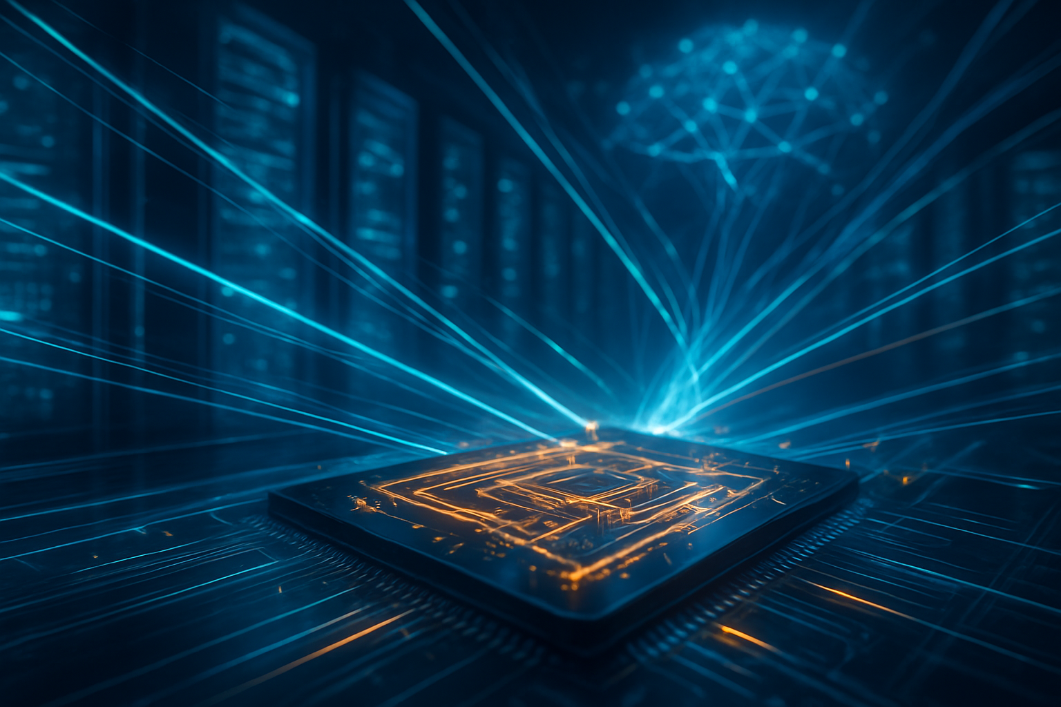
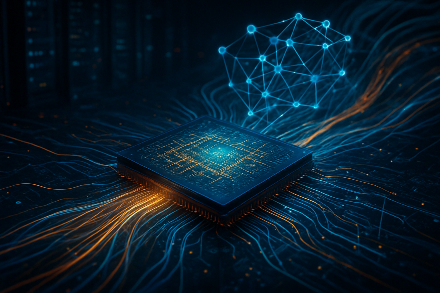
    The consumer electronics landscape shifted seismically this month at CES 2026, marking the definitive end of the "Chatbot Era" and the dawn of the "Agentic Era." For the last two years, the industry teased the potential of the AI PC, but the 2026 showcase in Las Vegas proved that the hardware has finally caught up to the hype. No longer restricted to simple text summaries or image generation, the latest silicon from the world’s leading chipmakers is now capable of running autonomous agents locally—systems that can plan, reason, and execute complex workflows across applications without ever sending a single packet of data to the cloud.

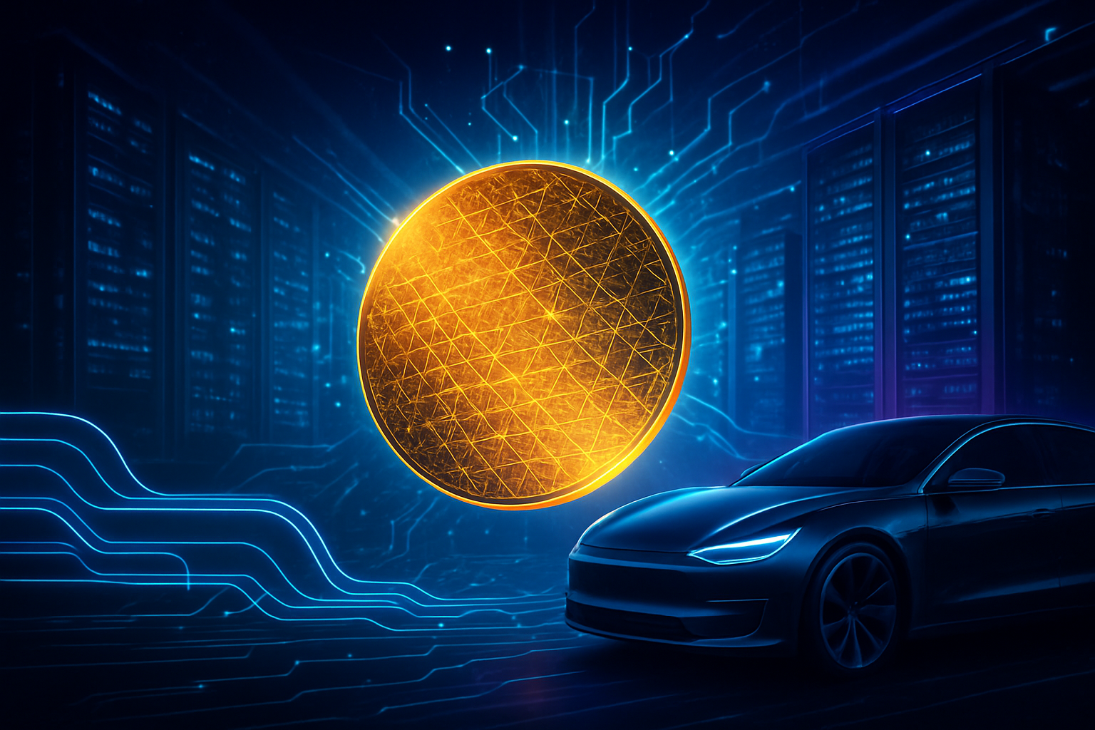
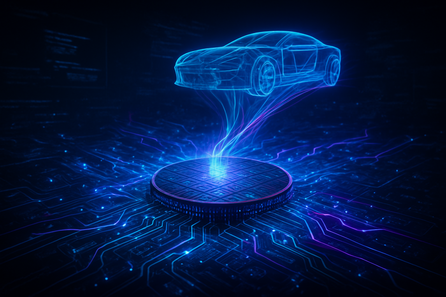
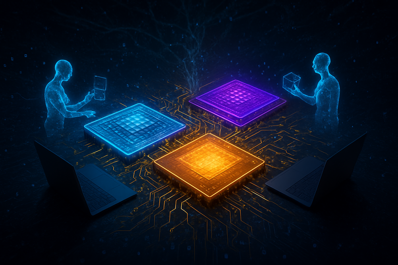
    This transition is underpinned by a brutal three-way war between Intel, Qualcomm, and AMD. As these titans unveiled their latest system-on-chips (SoCs), the metrics of success have shifted from raw clock speeds to NPU (Neural Processing Unit) TOPS (Trillions of Operations Per Second) and the ability to sustain high-parameter models on-device. With performance levels now hitting the 60-80 TOPS range for dedicated NPUs, the laptop has been reimagined as a private, sovereign AI node, fundamentally challenging the dominance of cloud-based AI providers.

    The Silicon Arms Race: Panther Lake, X2 Elite, and the Rise of 80 TOPS

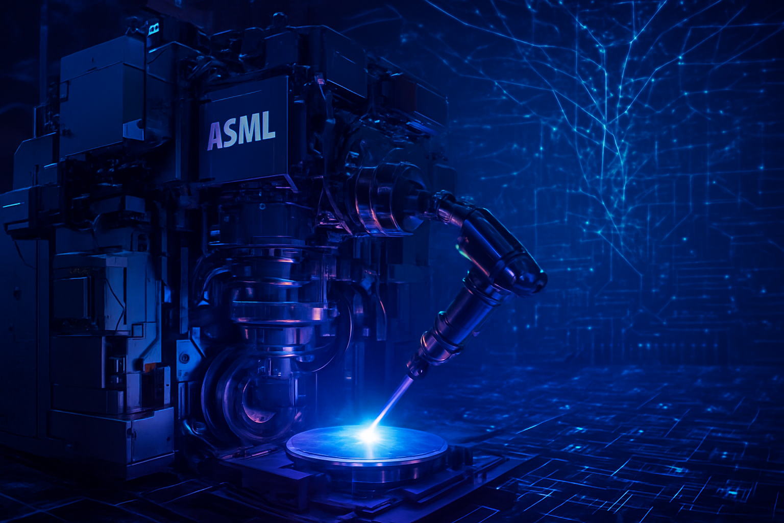
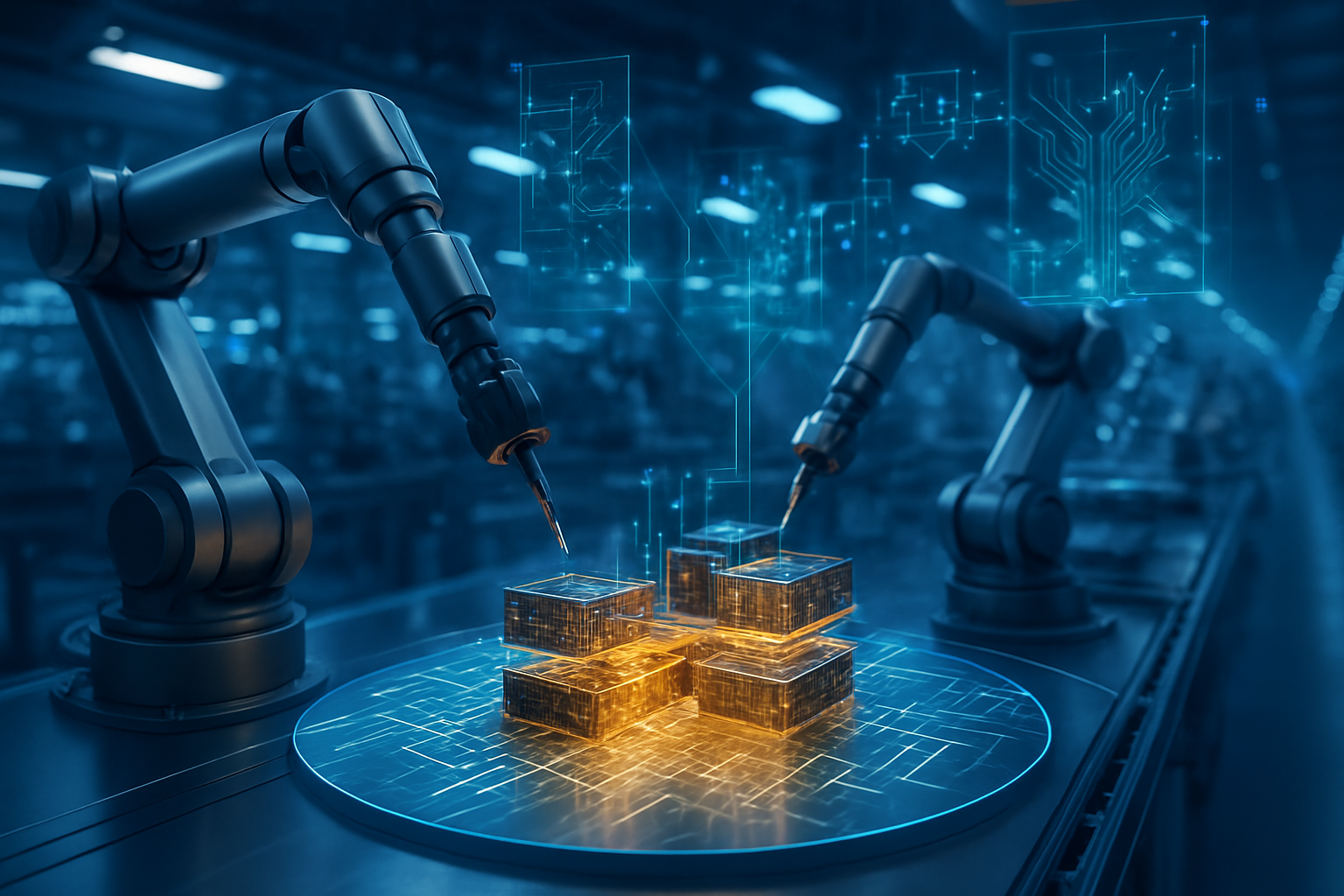
    The technical showdown at CES 2026 centered on three flagship architectures: Intel’s Panther Lake, Qualcomm’s Snapdragon X2 Elite, and AMD’s Ryzen AI 400. Intel Corporation (NASDAQ: INTC) took center stage with the launch of Panther Lake, branded as the Core Ultra Series 3. Built on the highly anticipated Intel 18A process node, Panther Lake represents a massive architectural leap, utilizing Cougar Cove performance cores and Darkmont efficiency cores. While its dedicated NPU 5 delivers 50 TOPS, Intel emphasized its "Platform TOPS" approach, leveraging the Xe3 (Celestial) graphics engine to reach a combined 180 TOPS. This allows Panther Lake machines to run Large Language Models (LLMs) with 30 to 70 billion parameters locally, a feat previously reserved for high-end desktop workstations.

    Qualcomm Inc. (NASDAQ: QCOM), however, currently holds the crown for raw NPU throughput. The newly unveiled Snapdragon X2 Elite, powered by the 3rd Generation Oryon CPU, features a Hexagon NPU capable of a staggering 80 TOPS. Qualcomm’s focus remained on power efficiency and "Ambient Intelligence," demonstrating a seamless integration with Google’s Gemini Nano to power proactive assistants. These agents don't wait for a prompt; they monitor user workflows in real-time to suggest actions, such as automatically drafting follow-up emails after a local voice call or organizing files based on the context of an ongoing project.

    Advanced Micro Devices, Inc. (NASDAQ: AMD) countered with the Ryzen AI 400 series (codenamed Gorgon Point). While its 60 TOPS XDNA 2 NPU sits in the middle of the pack, AMD’s strategy is built on accessibility and software ecosystem integration. By partnering with Nexa AI to launch "Hyperlink," an on-device agentic retrieval system, AMD is positioning itself as the leader in "Private Search." Hyperlink acts as a local version of Perplexity, indexing every document, chat, and file on a user’s hard drive to provide an agentic interface that can answer questions and perform tasks based on a user’s entire digital history without compromising privacy.

    Market Disruptions: Breaking the Cloud Chains

    This shift toward local Agentic AI has profound implications for the tech hierarchy. For years, the AI narrative was controlled by cloud giants who benefited from massive data center investments. However, the 2026 hardware cycle suggests a potential "de-clouding" of the AI industry. As NPUs become powerful enough to handle sophisticated reasoning tasks, the high latency and subscription costs associated with cloud-based LLMs become less attractive to both enterprises and individual users. Microsoft Corporation (NASDAQ: MSFT) has already pivoted to reflect this, announcing "Work IQ," a local memory feature for Copilot+ PCs that stores interaction history exclusively on-device.

    The competitive pressure is also forcing PC OEMs to differentiate through proprietary software layers rather than just hardware assembly. Lenovo Group Limited (HKG: 0992) introduced "Qira," a personal AI agent that maintains context across a user's phone, tablet, and PC. By leveraging the 60-80 TOPS available in new silicon, Qira can perform multi-step tasks—like booking a flight based on a calendar entry and an emailed preference—entirely within the local environment. This move signals a shift where the value proposition of a PC is increasingly defined by the quality of its resident "Super Agent" rather than just its screen or keyboard.

    For startups and software developers, this hardware opens a new frontier. The emergence of the Model Context Protocol (MCP) as an industry standard allows different local agents to communicate and share data securely. This enables a modular AI ecosystem where a specialized coding agent from a startup can collaborate with a scheduling agent from another provider, all running on a single Intel or Qualcomm chip. The strategic advantage is shifting toward those who can optimize models for NPU-specific execution, potentially disrupting the "one-size-fits-all" model of centralized AI.

    Privacy, Sovereignty, and the AI Landscape

    The broader significance of the 2026 AI PC war lies in the democratization of privacy. Previous AI breakthroughs, such as the release of GPT-4, required users to surrender their data to remote servers. The Agentic AI PCs showcased at CES 2026 flip this script. By providing 60-80 TOPS of local compute, these machines enable "Data Sovereignty." Users can now utilize the power of advanced AI for sensitive tasks—legal analysis, medical record management, or proprietary software development—without the risk of data leaks or the ethical concerns of training third-party models on their private information.

    Furthermore, this hardware evolution addresses the looming energy crisis facing the AI sector. Running agents locally on high-efficiency 3nm and 18A chips is significantly more energy-efficient than the massive overhead required to power hyperscale data centers. This "edge-first" approach to AI could be the key to scaling the technology sustainably. However, it also raises new concerns regarding the "digital divide." As the baseline for a functional AI PC moves toward expensive, high-TOPS silicon, there is a risk that those unable to afford the latest hardware from Intel or AMD will be left behind in an increasingly automated world.

    Comparatively, the leap from 2024’s 40 TOPS requirements to 2026’s 80 TOPS peak is more than just a numerical increase; it is a qualitative shift. It represents the move from AI as a "feature" (like a blur-background tool in a video call) to AI as the "operating system." In this new paradigm, the NPU is not a co-processor but the central intelligence that orchestrates the entire user experience.

    The Horizon: From 80 TOPS to Humanoid Integration

    Looking ahead, the momentum built at CES 2026 shows no signs of slowing. AMD has already teased its 2027 "Medusa" architecture, which is expected to utilize a 2nm process and push NPU performance well beyond the 100 TOPS mark. Intel’s 18A node is just the beginning of its "IDM 2.0" roadmap, with plans to integrate even deeper "Physical AI" capabilities that allow PCs to act as control hubs for household robotics and IoT ecosystems.

    The next major challenge for the industry will be memory bandwidth. While NPUs are becoming incredibly fast, the "memory wall" remains a bottleneck for running truly massive models. We expect the 2027 cycle to focus heavily on unified memory architectures and on-package LPDDR6 to ensure that the 80+ TOPS NPUs are never starved for data. As these hardware hurdles are cleared, the applications will evolve from simple productivity agents to "Digital Twins"—AI entities that can truly represent a user's professional persona in meetings or handle complex creative projects autonomously.

    Final Thoughts: The PC Reborn

    The 2026 AI PC war has effectively rebranded the personal computer. It is no longer a tool for consumption or manual creation, but a localized engine of autonomy. The competition between Intel, Qualcomm, and AMD has accelerated the arrival of Agentic AI by years, moving us into a world where our devices don't just wait for instructions—they participate in our work.

    The significance of this development in AI history cannot be overstated. We are witnessing the decentralization of intelligence. As we move into the spring of 2026, the industry will be watching closely to see which "Super Agents" gain the most traction with users. The hardware is here; the agents have arrived. The only question left is how much of our daily lives we are ready to delegate to the silicon sitting on our desks.


    This content is intended for informational purposes only and represents analysis of current AI developments.

    TokenRing AI delivers enterprise-grade solutions for multi-agent AI workflow orchestration, AI-powered development tools, and seamless remote collaboration platforms.
    For more information, visit https://www.tokenring.ai/.

  • The Power Behind the Intelligence: Wide-Bandgap Semiconductors to Top $5 Billion in 2026 as AI and EVs Converge

    The Power Behind the Intelligence: Wide-Bandgap Semiconductors to Top $5 Billion in 2026 as AI and EVs Converge

    The global semiconductor landscape is witnessing a seismic shift as 2026 marks the definitive "Wide-Bandgap (WBG) Era." Driven by the insatiable power demands of AI data centers and the wholesale transition of the automotive industry toward high-voltage architectures, the market for Silicon Carbide (SiC) and Gallium Nitride (GaN) discrete devices is projected to exceed $5.3 billion this year. This milestone represents more than just a fiscal achievement; it signals the end of silicon’s decades-long dominance in high-power applications, where its thermal and electrical limits have finally been reached by the sheer scale of modern computing.

    As of late January 2026, the industry is tracking a massive capacity build-out, with major manufacturers racing to bring new fabrication plants online. This surge is largely fueled by the realization that current AI hardware, despite its logical brilliance, is physically constrained by heat. By replacing traditional silicon with WBG materials, engineers are finding they can manage the immense thermal output of next-generation GPU clusters and EV inverters with unprecedented efficiency, effectively doubling down on the performance-per-watt metrics that now dictate market leadership.

    Technical Superiority and the Rise of the 8-Inch Wafer

    The technical transition at the heart of this growth centers on the physical properties of SiC and GaN compared to traditional Silicon (Si). Silicon Carbide boasts a thermal conductivity nearly 3.3 times higher than silicon, allowing it to dissipate heat far more effectively and operate at temperatures exceeding 200°C. Meanwhile, GaN’s superior electron mobility allows for switching frequencies in the megahertz range—significantly higher than silicon—which enables the use of much smaller passive components like inductors and capacitors. These properties are no longer just "nice-to-have" advantages; they are essential for the 800V Direct Current (DC) architectures now becoming the standard in both high-end electric vehicles and AI server racks.

    A cornerstone of the 2026 market expansion is the massive investment by ROHM Semiconductor ([TYO: 6963]). The company’s new Miyazaki Plant No. 2, a sprawling 230,000 m² facility, has officially entered its high-volume phase this year. This plant is a critical hub for the production of 8-inch (200mm) SiC substrates. Moving from 6-inch to 8-inch wafers is a technical hurdle that has historically plagued the industry, but the successful scaling at the Miyazaki and Chikugo plants has increased chip output per wafer by nearly 1.8x. This efficiency gain has been instrumental in driving down the cost of SiC devices, making them competitive with silicon-based Insulated Gate Bipolar Transistors (IGBTs) for the first time in mid-market applications.

    Initial reactions from the semiconductor research community have highlighted how these advancements solve the "thermal bottleneck" of modern AI. Recent tests of SiC-based power stages in server PSUs (Power Supply Units) have demonstrated peak efficiencies of 98%, a leap from the 94% ceiling typical of silicon. In the world of hyperscale data centers, that 4% difference translates into millions of dollars in saved electricity and cooling costs. Furthermore, NVIDIA ([NASDAQ: NVDA]) has reportedly begun exploring SiC interposers for its newest Blackwell-successor chips, aiming to reduce GPU operating temperatures by up to 20°C, which significantly extends the lifespan of the hardware under 24/7 AI training loads.

    Corporate Maneuvering and Market Positioning

    The surge in WBG demand has created a clear divide between companies that secured their supply chains early and those now scrambling for capacity. STMicroelectronics ([NYSE: STM]) and Infineon Technologies ([ETR: IFX]) continue to hold dominant positions, but the aggressive expansion of ROHM and Wolfspeed ([NYSE: WOLF]) has intensified the competitive landscape. These companies are no longer just component suppliers; they are strategic partners for the world’s largest tech and automotive giants. For instance, BYD ([HKG: 1211]) and Hyundai Motor Company ([KRX: 005380]) have integrated SiC into their 2026 vehicle lineups to achieve a 5-10% range increase without increasing battery size, a move that provides a massive competitive edge in the price-sensitive EV market.

    In the data center space, the impact is equally transformative. Major cloud providers are shifting toward 800V high-voltage direct current architectures to power their AI clusters. This has benefited companies like Lucid Motors ([NASDAQ: LCID]), which has leveraged its expertise in high-voltage power electronics to consult on industrial power management. The strategic advantage now lies in "vertical integration"—those who control the substrate production (the raw SiC or GaN material) are less vulnerable to the price volatility and shortages that defined the early 2020s.

    Wider Significance: Energy, AI, and Global Sustainability

    The transition to WBG semiconductors represents a critical pivot in the global AI landscape. As concerns grow regarding the environmental impact of AI—specifically the massive energy consumption of large language model (LLM) training—SiC and GaN offer a tangible path toward "Greener AI." By reducing switching losses and improving thermal management, these materials are estimated to reduce the carbon footprint of a 10MW data center by nearly 15% annually. This aligns with broader ESG goals while simultaneously allowing companies to pack more compute power into the same physical footprint.

    However, the rapid growth also brings potential concerns, particularly regarding the complexity of the manufacturing process. SiC crystals are notoriously difficult to grow, requiring temperatures near 2,500°C and specialized furnaces. Any disruption in the supply of high-purity graphite or specialized silicon carbide powder could create a bottleneck that slows the deployment of AI infrastructure. Comparisons are already being made to the 2021 chip shortage, with analysts warning that the "Power Gap" might become the next "Memory Gap" in the tech industry’s race toward artificial general intelligence.

    The Horizon: 12-Inch Wafers and Ultra-Fast Charging

    Looking ahead, the industry is already eyeing the next frontier: 12-inch (300mm) SiC production. While 8-inch wafers are the current state-of-the-art in 2026, R&D labs at ROHM and Wolfspeed are reportedly making progress on larger formats that could further slash costs by 2028. We are also seeing the rise of "GaN-on-SiC" and "GaN-on-GaN" technologies, which aim to combine the high-frequency benefits of Gallium Nitride with the superior thermal dissipation of Silicon Carbide for ultra-dense AI power modules.

    On the consumer side, the proliferation of these materials will soon manifest in 350kW+ ultra-fast charging stations, capable of charging an EV to 80% in under 10 minutes without overheating. Experts predict that by 2027, the use of WBG semiconductors will be so pervasive that traditional silicon power devices will be relegated to low-power, "legacy" electronics. The primary challenge remains the development of standardized testing protocols for these materials, as their long-term reliability in the extreme environments of an AI server or a vehicle drivetrain is still being documented in real-time.

    Conclusion: A Fundamental Shift in Power

    The 2026 milestone of a $5 billion market for SiC and GaN discrete devices marks a fundamental shift in how we build the world’s most advanced machines. From the silicon-carbide-powered inverters in our cars to the gallium-nitride-cooled servers processing our queries, WBG materials have moved from a niche laboratory curiosity to the backbone of the global digital and physical infrastructure.

    As we move through the remainder of 2026, the key developments to watch will be the output yield of ROHM’s Miyazaki plant and the potential for a "Power-Efficiency War" between AI labs. In a world where intelligence is limited by the power you can provide and the heat you can remove, the masters of wide-bandgap semiconductors may very well hold the keys to the future of AI development.


    This content is intended for informational purposes only and represents analysis of current AI developments.

    TokenRing AI delivers enterprise-grade solutions for multi-agent AI workflow orchestration, AI-powered development tools, and seamless remote collaboration platforms.
    For more information, visit https://www.tokenring.ai/.

  • The High-NA Era Arrives: How Intel’s $380M Lithography Bet is Redefining AI Silicon

    The High-NA Era Arrives: How Intel’s $380M Lithography Bet is Redefining AI Silicon

    The dawn of 2026 marks a historic inflection point in the semiconductor industry as the "mass production era" of High-Numerical Aperture (High-NA) Extreme Ultraviolet (EUV) lithography officially moves from laboratory speculation to the factory floor. Leading the charge, Intel (NASDAQ: INTC) has confirmed the completion of acceptance testing for its latest fleet of ASML (NASDAQ: ASML) Twinscan EXE:5200 systems, signaling the start of a multi-year transition toward the 1.4nm (14A) node. With each machine carrying a price tag exceeding $380 million, this development represents one of the most expensive and technically demanding gambles in industrial history, aimed squarely at sustaining the hardware requirements of the generative AI revolution.

    The significance of this transition cannot be overstated for the future of artificial intelligence. As transformer models grow in complexity, the demand for processors with higher transistor densities and lower power profiles has hit a physical wall with traditional EUV technology. By deploying High-NA tools, chipmakers are now able to print features with a resolution of approximately 8nm—nearly doubling the precision of previous generations. This shift is not merely an incremental upgrade; it is a fundamental reconfiguration of the economics of scaling, moving the industry toward a future where 1nm processors will eventually power the next decade of autonomous systems and trillion-parameter AI models.

    The Physics of 0.55 NA: A New Blueprint for Transistors

    At the heart of this revolution is ASML’s Twinscan EXE series, which increases the Numerical Aperture (NA) from 0.33 to 0.55. In practical terms, this allows the lithography machine to focus light more sharply, enabling the printing of significantly smaller features on a silicon wafer. While standard EUV tools required "multi-patterning"—a process of printing a single layer multiple times to achieve higher resolution—High-NA EUV enables single-exposure patterning for the most critical layers of a chip. This reduction in process complexity is expected to improve yields and shorten the time-to-market for cutting-edge AI accelerators, which have historically been plagued by the intricate manufacturing requirements of sub-3nm nodes.

    Technically, the transition to High-NA introduces an "anamorphic" optical system, which magnifies the X and Y axes differently. This design results in a "half-field" exposure, meaning the reticle size is effectively halved compared to standard EUV. To manufacture the massive dies required for high-end AI GPUs, such as those produced by NVIDIA (NASDAQ: NVDA), manufacturers must now employ "stitching" techniques to join two exposure fields into a single seamless pattern. This architectural shift has sparked intense discussion among AI researchers and hardware engineers, as it necessitates a move toward "chiplet" designs where multiple smaller dies are interconnected, rather than relying on a single monolithic slab of silicon.

    Intel’s primary vehicle for this technology is the 14A node, the world’s first process built from the ground up to be "High-NA native." Initial reports from Intel’s D1X facility in Oregon suggest that the EXE:5200B tools are achieving throughputs of over 220 wafers per hour, a critical metric for high-volume manufacturing. Industry experts note that while the $380 million capital expenditure per tool is staggering, the ability to eliminate multiple mask steps in the production cycle could eventually offset these costs, provided the volume of AI-specific silicon remains high.

    A High-Stakes Rivalry: Intel vs. Samsung and the "Lithography Divide"

    The deployment of High-NA EUV has created a strategic divide among the world’s three leading foundries. Intel’s aggressive "first-mover" advantage is a calculated attempt to regain process leadership after losing ground to competitors over the last decade. By securing the earliest shipments of the EXE:5200 series, Intel is positioning itself as the premier destination for custom AI silicon from tech giants like Microsoft (NASDAQ: MSFT) and Amazon (NASDAQ: AMZN), who are increasingly looking to design their own proprietary chips to optimize AI workloads.

    Samsung (KRX: 005930), meanwhile, has taken a dual-track approach. Having received its first High-NA units in 2025, the South Korean giant is integrating the technology into both its logic foundry and its advanced memory production. For Samsung, High-NA is essential for the development of HBM4 (High Bandwidth Memory), the specialized memory that feeds data to AI processors. The precision of High-NA is vital for the extreme vertical stacking required in next-generation HBM, making Samsung a formidable competitor in the AI hardware supply chain.

    In contrast, Taiwan Semiconductor Manufacturing Company (NYSE: TSM) has maintained a more conservative stance, opting to refine its existing 0.33 NA EUV processes for its 2nm (N2) node. This has created a "lithography divide" where Intel and Samsung are betting on the raw resolution of High-NA, while TSMC relies on its proven manufacturing excellence and cost-efficiency. The competitive implication is clear: if High-NA enables Intel to hit the 1.4nm milestone ahead of schedule, the balance of power in the global semiconductor market could shift back toward American and Korean soil for the first time in years.

    Moore’s Law and the Energy Crisis of AI

    The broader significance of the High-NA era lies in its role as a "lifeline" for Moore’s Law. For years, critics have predicted the end of transistor scaling, arguing that the heat and physical limitations of sub-atomically small components would eventually halt progress. High-NA EUV, combined with new transistor architectures like Gate-All-Around (GAA) and backside power delivery, provides a roadmap for another decade of scaling. This is particularly vital as the AI landscape shifts from "training" large models to "inference" at the edge, where energy efficiency is the primary constraint.

    Processors manufactured on the 1.4nm and 1nm nodes are expected to deliver up to a 30% reduction in power consumption compared to current 3nm chips. In an era where AI data centers are consuming an ever-larger share of the global power grid, these efficiency gains are not just an economic advantage—they are a geopolitical and environmental necessity. Without the scaling enabled by High-NA, the projected growth of generative AI would likely be throttled by the sheer energy requirements of the hardware needed to support it.

    However, the transition is not without its concerns. The extreme cost of High-NA tools threatens to centralize chip manufacturing even further, as only a handful of companies can afford the multi-billion dollar investment required to build a High-NA-capable "mega-fab." This concentration of advanced manufacturing capabilities raises questions about supply chain resilience and the accessibility of cutting-edge hardware for smaller AI startups. Furthermore, the technical challenges of "stitching" half-field exposures could lead to initial yield issues, potentially keeping prices high for the very AI chips the technology is meant to proliferate.

    The Road to 1.4nm and Beyond

    Looking ahead, the next 24 to 36 months will be focused on perfecting the transition from pilot production to High-Volume Manufacturing (HVM). Intel is targeting 2027 for the full commercialization of its 14A node, with Samsung likely following closely behind with its SF1.4 process. Beyond that, the industry is already eyeing the 1nm milestone—often referred to as the "Angstrom era"—where features will be measured at the scale of individual atoms.

    Future developments will likely involve the integration of High-NA with even more exotic materials and architectures. We can expect to see the rise of "2D semiconductors" and "carbon nanotube" components that take advantage of the extreme resolution provided by ASML’s optics. Additionally, as the physical limits of light-based lithography are reached, researchers are already exploring "Hyper-NA" systems with even higher apertures, though such technology remains in the early R&D phase.

    The immediate challenge remains the optimization of the photoresist chemicals and mask technology used within the High-NA machines. At such small scales, "stochastic effects"—random variations in the way light interacts with matter—become a major source of defects. Solving these material science puzzles will be the primary focus of the engineering community throughout 2026, as they strive to make the 1.4nm roadmap a reality for the mass market.

    A Watershed Moment for AI Infrastructure

    The arrival of the High-NA EUV mass production era is a watershed moment for the technology industry. It represents the successful navigation of one of the most difficult engineering hurdles in human history, ensuring that the physical hardware of the AI age can continue to evolve alongside the software. For Intel, it is a "do-or-die" moment to reclaim its crown; for Samsung, it is an opportunity to dominate both the brain (logic) and the memory of future AI systems.

    In summary, the transition to 0.55 NA lithography marks the end of the "low-resolution" era of semiconductor manufacturing. While the $380 million price tag per machine is a barrier to entry, the potential for 2.9x increases in transistor density offers a clear path toward the 1.4nm and 1nm chips that will define the late 2020s. The industry has effectively doubled down on hardware scaling to meet the insatiable appetite of AI.

    In the coming months, watchers should keep a close eye on the first "test chips" emerging from Intel’s 14A pilot lines. The success or failure of these early runs will dictate the pace of AI hardware advancement for the rest of the decade. As the first High-NA-powered processors begin to power the next generation of data centers, the true impact of this $380 million gamble will finally be revealed in the speed and efficiency of the AI models we use every day.


    This content is intended for informational purposes only and represents analysis of current AI developments.

    TokenRing AI delivers enterprise-grade solutions for multi-agent AI workflow orchestration, AI-powered development tools, and seamless remote collaboration platforms.
    For more information, visit https://www.tokenring.ai/.

  • The Great Unclogging: TSMC Commits $56 Billion Capex to Double CoWoS Capacity for NVIDIA’s Rubin Era

    The Great Unclogging: TSMC Commits $56 Billion Capex to Double CoWoS Capacity for NVIDIA’s Rubin Era

    TAIPEI, Taiwan — In a definitive move to cement its dominance over the global AI supply chain, Taiwan Semiconductor Manufacturing Company (NYSE: TSM) has officially entered a "capex supercycle," announcing a staggering $52 billion to $56 billion capital expenditure budget for 2026. The announcement, delivered during the company's January 15 earnings call, signals the end of the "Great AI Hardware Bottleneck" that has plagued the industry for the better part of three years. By scaling its proprietary CoWoS (Chip-on-Wafer-on-Substrate) advanced packaging capacity to a projected 130,000—and potentially 150,000—wafers per month by late 2026, TSMC is effectively industrializing the production of next-generation AI accelerators.

    This massive expansion is largely a response to "insane" demand from NVIDIA (NASDAQ: NVDA), which has reportedly secured over 60% of TSMC’s 2026 packaging capacity to support the launch of its Rubin architecture. As AI models grow in complexity, the industry is shifting away from monolithic chips toward "chiplets," making advanced packaging—once a niche back-end process—the most critical frontier in semiconductor manufacturing. TSMC’s strategic pivot treats packaging not as an afterthought, but as a primary revenue driver that is now fundamentally inseparable from the fabrication of the world’s most advanced 2nm and A16 nodes.

    Breaking the Reticle Limit: The Rise of CoWoS-L

    The technical centerpiece of this expansion is CoWoS-L (Local Silicon Interconnect), a sophisticated packaging technology designed to bypass the physical limitations of traditional silicon manufacturing. In standard chipmaking, the "reticle limit" defines the maximum size of a single chip (roughly 858mm²). However, NVIDIA’s upcoming Rubin (R100) GPUs and the current Blackwell Ultra (B300) series require a surface area far larger than any single piece of silicon can provide. CoWoS-L solves this by using small silicon "bridges" embedded in an organic layer to interconnect multiple compute dies and High Bandwidth Memory (HBM) stacks.

    Unlike the older CoWoS-S, which used a solid silicon interposer and was limited in size and yield, CoWoS-L allows for massive "Superchips" that can be up to six times the standard reticle size. This enables NVIDIA to "stitch" together its GPU dies with 12 or even 16 stacks of next-generation HBM4 memory, providing the terabytes of bandwidth required for trillion-parameter AI models. Industry experts note that the transition to CoWoS-L is technically demanding; during a recent media tour of TSMC’s new Chiayi AP7 facility on January 22, engineers highlighted that the alignment precision required for these silicon bridges is measured in nanometers, representing a quantum leap over the packaging standards of just two years ago.

    The "Compute Moat": Consolidating the AI Hierarchy

    TSMC’s capacity expansion creates a strategic "compute moat" for its largest customers, most notably NVIDIA. By pre-booking the lion's share of the 130,000 monthly wafers, NVIDIA has effectively throttled the ability of competitors like AMD (NASDAQ: AMD) and Intel (NASDAQ: INTC) to scale their own high-end AI offerings. While AMD’s Instinct MI400 series is expected to utilize similar packaging techniques, the sheer volume of TSMC’s commitment to NVIDIA suggests that "Team Green" will maintain its lead in time-to-market for the Rubin R100, which is slated for full production in late 2026.

    This expansion also benefits "hyperscale" custom silicon designers. Companies like Broadcom (NASDAQ: AVGO) and Marvell (NASDAQ: MRVL), which design bespoke AI chips for Google (NASDAQ: GOOGL) and Amazon (NASDAQ: AMZN), are also vying for a slice of the CoWoS-L pie. However, the $56 billion capex plan underscores a shift in power: TSMC is no longer just a "dumb pipe" for wafer fabrication; it is the gatekeeper of AI performance. Startups and smaller chip designers may find themselves pushed toward Outsourced Semiconductor Assembly and Test (OSAT) partners like Amkor Technology (NASDAQ: AMKR), as TSMC prioritizes high-margin, high-complexity orders from the "Big Three" of AI.

    The Geopolitics of the Chiplet Era

    The broader significance of TSMC’s 2026 roadmap lies in the realization that the "Chiplet Era" is officially here. We are witnessing a fundamental change in the semiconductor landscape where performance gains are coming from how chips are assembled, rather than just how small their transistors are. This shift has profound implications for global supply chain stability. By concentrating its advanced packaging facilities in sites like Chiayi and Taichung, TSMC is centralizing the world’s AI "brain" production. While this provides unprecedented efficiency, it also heightens the stakes for geopolitical stability in the Taiwan Strait.

    Furthermore, the easing of the CoWoS bottleneck marks a transition from a "supply-constrained" AI market to a "demand-validated" one. For the past two years, AI growth was limited by how many GPUs could be built; by 2026, the limit will be how much power data centers can draw and how efficiently developers can utilize the massive compute pools being deployed. The transition to HBM4, which requires the complex interfaces provided by CoWoS-L, will be the true test of this new infrastructure, potentially leading to a 3x increase in memory bandwidth for LLM (Large Language Model) training compared to 2024 levels.

    The Horizon: Panel-Level Packaging and Beyond

    Looking beyond the 130,000 wafer-per-month milestone, the industry is already eyeing the next frontier: Panel-Level Packaging (PLP). TSMC has begun pilot-testing rectangular "Panel" substrates, which offer three to four times the usable surface area of a traditional 300mm circular wafer. If successful, this could further reduce costs and increase the output of AI chips in 2027 and 2028. Additionally, the integration of "Glass Substrates" is on the long-term roadmap, promising even higher thermal stability and interconnect density for the post-Rubin era.

    Challenges remain, particularly in power delivery and heat dissipation. As CoWoS-L allows for larger and hotter chip clusters, TSMC and its partners are heavily investing in liquid cooling and "on-chip" power management solutions. Analysts predict that by late 2026, the focus of the AI hardware race will shift from "packaging capacity" to "thermal management efficiency," as the industry struggles to keep these multi-thousand-watt monsters from melting.

    Summary and Outlook

    TSMC’s $56 billion capex and its 130,000-wafer CoWoS target represent a watershed moment for the AI industry. It is a massive bet on the longevity of the AI boom and a vote of confidence in NVIDIA’s Rubin roadmap. The move effectively ends the era of hardware scarcity, potentially lowering the barrier to entry for large-scale AI deployment while simultaneously concentrating power in the hands of the few companies that can afford TSMC’s premium services.

    As we move through 2026, the key metrics to watch will be the yield rates of the new Chiayi AP7 facility and the first real-world performance benchmarks of HBM4-equipped Rubin GPUs. For now, the message from Taipei is clear: the bottleneck is breaking, and the next phase of the AI revolution will be manufactured at a scale never before seen in human history.


    This content is intended for informational purposes only and represents analysis of current AI developments.

    TokenRing AI delivers enterprise-grade solutions for multi-agent AI workflow orchestration, AI-powered development tools, and seamless remote collaboration platforms.
    For more information, visit https://www.tokenring.ai/.

  • The Silicon Renaissance: How AI-Led EDA Tools are Redefining Chip Design at CES 2026

    The Silicon Renaissance: How AI-Led EDA Tools are Redefining Chip Design at CES 2026

    The traditional boundaries of semiconductor engineering were shattered this month at CES 2026, as the industry pivoted from human-centric chip design to a new era of "AI-defined" hardware. Leading the charge, Electronic Design Automation (EDA) giants demonstrated that the integration of generative AI and reinforcement learning into the silicon lifecycle is no longer a luxury but a fundamental necessity for survival. By automating the most complex phases of design, these tools are now delivering the impossible: reducing development timelines from months to mere weeks while slashing prototyping costs by 20% to 60%.

    The significance of this shift cannot be overstated. As the physical limits of Moore’s Law loom, the industry has found a new tailwind in software intelligence. The transformation is particularly visible in the automotive and high-performance computing sectors, where the need for bespoke, AI-optimized silicon has outpaced the capacity of human engineering teams. With the debut of new virtualized ecosystems and "agentic" design assistants, the barriers to entry for custom silicon are falling, ushering in a "Silicon Renaissance" that promises to accelerate innovation across every vertical of the global economy.

    The Technical Edge: Arm Zena and the Virtualization Revolution

    At the heart of the announcements at CES 2026 was the deep integration between Synopsys (Nasdaq: SNPS) and Arm (Nasdaq: ARM). Synopsys unveiled its latest Virtualizer Development Kits (VDKs) specifically optimized for the Arm Zena Compute Subsystem (CSS). The Zena CSS is a marvel of modular engineering, featuring a 16-core Arm Cortex-A720AE cluster and a dedicated "Safety Island" for real-time diagnostics. By using Synopsys VDKs, automotive engineers can now create a digital twin of the Zena hardware. This allows software teams to begin writing and testing code for next-generation autonomous driving features up to a year before the actual physical silicon returns from the foundry—a practice known as "shifting left."

    Meanwhile, Cadence Design Systems (Nasdaq: CDNS) showcased its own breakthroughs in engineering virtualization through the Helium Virtual and Hybrid Studio. Cadence's approach focuses on "Physical AI," where chiplet-based designs are validated within a virtual environment that mirrors the exact performance characteristics of the target hardware. Their partner ecosystem, which includes Samsung Electronics (OTC: SSNLF) and Arteris (Nasdaq: AIPRT), demonstrated how pre-validated chiplets could be assembled like Lego blocks. This modularity, combined with Cadence’s Cerebrus AI, allows for the autonomous optimization of "Power, Performance, and Area" (PPA), evaluating $10^{90,000}$ design permutations to find the most efficient layout in a fraction of the time previously required.

    The most startling technical metric shared during the summit was the impact of Generative AI on floorplanning—the process of arranging circuits on a silicon die. What used to be a grueling, multi-month iterative process for teams of senior engineers is now being handled by AI agents like Synopsys.ai Copilot. These agents analyze historical design data and real-time constraints to produce optimized layouts in days. The resulting 20-60% reduction in costs stems from fewer "respins" (expensive design corrections) and a significantly reduced need for massive, specialized engineering cohorts for routine optimization tasks.

    Competitive Landscapes and the Rise of the Hyperscalers

    The democratization of high-end chip design through AI-led EDA tools is fundamentally altering the competitive landscape. Traditionally, only giants like Nvidia (Nasdaq: NVDA) or Apple (Nasdaq: AAPL) had the resources to design world-class custom silicon. Today, the 20-60% cost reduction and timeline compression mean that mid-tier automotive OEMs and startups can realistically pursue custom SoCs (System on Chips). This shifts the power dynamic away from general-purpose chip makers and toward those who can design specific hardware for specific AI workloads.

    Cloud providers are among the biggest beneficiaries of this shift. Amazon (Nasdaq: AMZN) and Microsoft (Nasdaq: MSFT) are already leveraging these AI-driven tools to accelerate their internal silicon roadmaps, such as the Graviton and Maia series. By utilizing the "ISA parity" offered by the Arm Zena ecosystem, these hyperscalers can provide developers with a seamless environment where code written in the cloud runs identically on edge devices. This creates a feedback loop that strengthens the grip of cloud giants on the AI development pipeline, as they now provide both the software tools and the optimized hardware blueprints.

    Foundries and specialized chip makers are also repositioning themselves. NXP Semiconductors (Nasdaq: NXPI) and Texas Instruments (Nasdaq: TXN) have integrated Synopsys VDKs into their workflows to better serve the "Software-Defined Vehicle" (SDV) market. By providing virtual models of their upcoming chips, they lock in automotive manufacturers earlier in the design cycle. This creates a "virtual-first" sales model where the software environment is as much a product as the physical silicon, making it increasingly difficult for legacy players who lack a robust AI-EDA strategy to compete.

    Beyond the Die: The Global Significance of AI-Led EDA

    The transformation of chip design carries weight far beyond the technical community; it is a geopolitical and economic milestone. As nations race for "chip sovereignty," the ability to design high-performance silicon locally—without a decades-long heritage of manual engineering expertise—is a game changer. AI-led EDA tools act as a "force multiplier," allowing smaller nations and regional hubs to establish viable semiconductor design sectors. This could lead to a more decentralized global supply chain, reducing the world's over-reliance on a handful of design houses in Silicon Valley.

    However, this rapid advancement is not without its concerns. The automation of complex engineering tasks raises questions about the future of the semiconductor workforce. While the industry currently faces a talent shortage, the transition from months to weeks in design cycles suggests that the role of the "human-in-the-loop" is shifting toward high-level architectural oversight rather than hands-on optimization. There is also the "black box" problem: as AI agents generate increasingly complex layouts, ensuring the security and verifiability of these designs becomes a paramount challenge for mission-critical applications like aerospace and healthcare.

    Comparatively, this breakthrough mirrors the transition from assembly language to high-level programming in the 1970s. Just as compilers allowed software to scale exponentially, AI-led EDA is providing the "silicon compiler" that the industry has sought for decades. It marks the end of the "hand-crafted" era of chips and the beginning of a generative era where hardware can evolve as rapidly as the software that runs upon it.

    The Horizon: Agentic EDA and Autonomous Foundries

    Looking ahead, the next frontier is "Agentic EDA," where AI systems do not just assist engineers but proactively manage the entire design-to-manufacturing pipeline. Experts predict that by 2028, we will see the first "lights-out" chip design projects, where the entire process—from architectural specification to GDSII (the final layout file for the foundry)—is handled by a swarm of specialized AI agents. These agents will be capable of real-time negotiation with foundry capacity, automatically adjusting designs based on available manufacturing nodes and material costs.

    We are also on the cusp of seeing AI-led design move into more exotic territories, such as photonic and quantum computing chips. The complexity of routing light or managing qubits is a perfect use case for the reinforcement learning models currently being perfected for silicon. As these tools mature, they will likely be integrated into broader industrial metaverses, where a car's entire electrical architecture, chassis, and software are co-optimized by a single, unified AI orchestrator.

    A New Era for Innovation

    The announcements from Synopsys, Cadence, and Arm at CES 2026 have cemented AI's role as the primary architect of the digital future. The ability to condense months of work into weeks and slash costs by up to 60% represents a permanent shift in how humanity builds technology. This "Silicon Renaissance" ensures that the explosion of AI software will be met with a corresponding leap in hardware efficiency, preventing a "compute ceiling" from stalling progress.

    As we move through 2026, the industry will be watching the first production vehicles and servers born from these virtualized AI workflows. The success of the Arm Zena CSS and the widespread adoption of Synopsys and Cadence’s generative tools will serve as the benchmark for the next decade of engineering. The hardware world is finally moving at the speed of software, and the implications for the future of artificial intelligence are limitless.


    This content is intended for informational purposes only and represents analysis of current AI developments.

    TokenRing AI delivers enterprise-grade solutions for multi-agent AI workflow orchestration, AI-powered development tools, and seamless remote collaboration platforms.
    For more information, visit https://www.tokenring.ai/.

  • The 1.6T Surge: Silicon Photonics and CPO Redefine AI Data Centers in 2026

    The 1.6T Surge: Silicon Photonics and CPO Redefine AI Data Centers in 2026

    The artificial intelligence industry has reached a critical infrastructure pivot as 2026 marks the year that light-based interconnects officially take the throne from traditional electrical wiring. According to a landmark report from Nomura, the market for 1.6T optical modules is experiencing an unprecedented "supercycle," with shipments expected to explode from 2.5 million units last year to a staggering 20 million units in 2026. This massive volume surge is being accompanied by a fundamental shift in how chips communicate, as Silicon Photonics (SiPh) penetration is projected to hit between 50% and 70% in the high-end 1.6T segment.

    This transition is not merely a speed upgrade; it is a survival necessity for the world's most advanced AI "gigascale" factories. As NVIDIA (NASDAQ: NVDA) and Broadcom (NASDAQ: AVGO) race to deploy the next generation of 102.4T switching fabrics, the limitations of traditional pluggable copper and electrical interconnects have become a "power wall" that only photonics can scale. By integrating optical engines directly onto the processor package—a process known as Co-Packaged Optics (CPO)—the industry is slashing power consumption and latency at a moment when data center energy demands have become a global economic concern.

    Breaking the 1.6T Barrier: The Shift to Silicon Photonics and CPO

    The technical backbone of this 2026 surge is the 1.6T optical module, a breakthrough that doubles the bandwidth of the previous 800G standard while significantly improving efficiency. Traditional optical modules relied heavily on Indium Phosphide (InP) or Vertical-Cavity Surface-Emitting Lasers (VCSELs). However, as we move into 2026, Silicon Photonics has become the dominant architecture. By leveraging mature CMOS manufacturing processes—the same used to build microchips—SiPh allows for the integration of complex optical functions onto a single silicon die. This reduces manufacturing costs and improves reliability, enabling the 50-70% market penetration rate forecasted by Nomura.

    Beyond simple modules, the industry is witnessing the commercial debut of Co-Packaged Optics (CPO). Unlike traditional pluggable optics that sit at the edge of a switch or server, CPO places the optical engines in the same package as the ASIC or GPU. This drastically shortens the electrical path that signals must travel. In traditional layouts, electrical path loss can reach 20–25 dB; with CPO, that loss is reduced to approximately 4 dB. This efficiency gain allows for higher signal integrity and, crucially, a reduction in the power required to drive data across the network.

    Initial reactions from the AI research community and networking architects have been overwhelmingly positive, particularly regarding the ability to maintain signal stability at 200G SerDes (Serializer/Deserializer) speeds. Analysts note that without the transition to SiPh and CPO, the thermal management of 1.6T systems would have been nearly impossible under current air-cooled or even early liquid-cooled standards.

    The Titans of Throughput: Broadcom and NVIDIA Lead the Charge

    The primary catalysts for this optical revolution are the latest platforms from Broadcom and NVIDIA. Broadcom (NASDAQ: AVGO) has solidified its leadership in the Ethernet space with the volume shipping of its Tomahawk 6 (TH6) switch, also known as the "Davisson" platform. The TH6 is the world’s first single-chip 102.4 Tbps Ethernet switch, incorporating sixteen 6.4T optical engines directly on the package. By moving the optics closer to the "brain" of the switch, Broadcom has managed to maintain an open ecosystem, partnering with box builders like Celestica (NYSE: CLS) and Accton to deliver standardized CPO solutions to hyperscalers.

    NVIDIA (NASDAQ: NVDA), meanwhile, is leveraging CPO to redefine its "scale-up" architecture—the high-speed fabric that connects thousands of GPUs into a single massive supercomputer. The newly unveiled Quantum-X800 CPO InfiniBand platform delivers a total capacity of 115.2 Tbps. By utilizing four 28.8T switch ASICs surrounded by optical engines, NVIDIA has slashed per-port power consumption from 30W in traditional pluggable setups to just 9W. This shift is integral to NVIDIA’s Rubin GPU architecture, launching in the second half of 2026, which relies on the ConnectX-9 SuperNIC to achieve 1.6 Tbps scale-out speeds.

    The supply chain is also undergoing a massive realignment. Manufacturers like InnoLight (SZSE: 300308) and Taiwan Semiconductor Manufacturing Company (NYSE: TSM) are seeing record demand for optical engines and specialized packaging services. The move toward CPO effectively shifts the value chain, as the distinction between a "chip company" and an "optical company" blurs, giving an edge to those who control the integration and packaging processes.

    Scaling the Power Wall: Why Optics Matter for the Global AI Landscape

    The surge in SiPh and CPO is more than a technical milestone; it is a response to the "power wall" that threatened to stall AI progress in 2025. As AI models have grown in size, the energy required to move data between GPUs has begun to rival the energy required for the actual computation. In 2026, data centers are increasingly mandated to meet strict efficiency targets, making the roughly 70% power reduction offered by CPO a critical business advantage rather than a luxury.

    This shift also marks a move toward "liquid-cooled everything." The extreme power density of CPO-based switches like the Quantum-X800 and Broadcom’s Tomahawk 6 makes traditional fan cooling obsolete. This has spurred a secondary boom in liquid-cooling infrastructure, further differentiating the modern "AI Factory" from the traditional data centers of the early 2020s.

    Furthermore, the 2026 transition to 1.6T and SiPh is being compared to the transition from copper to fiber in telecommunications decades ago. However, the stakes are higher. The competitive advantage of major AI labs now depends on "networking-to-compute" ratios. If a lab cannot move data fast enough across its cluster, its multi-billion dollar GPU investment sits idle. Consequently, the adoption of CPO has become a strategic imperative for any firm aiming for Tier-1 AI status.

    The Road to 3.2T and Beyond: What Lies Ahead

    Looking past 2026, the roadmap for optical interconnects points toward even deeper integration. Experts predict that by 2028, we will see the emergence of 3.2T optical modules and the eventual integration of "optical I/O" directly into the GPU die itself, rather than just in the same package. This would effectively eliminate the distinction between electrical and optical signals within the server rack, moving toward a "fully photonic" data center architecture.

    However, challenges remain. Despite the surge in capacity, the market still faces a 5-15% supply deficit in high-end optical components like CW (Continuous Wave) lasers. The complexity of repairing a CPO-enabled switch—where a failure in an optical engine might require replacing the entire $100,000+ switch ASIC—remains a concern for data center operators. Industry standards groups are currently working on "pluggable" light sources to mitigate this risk, allowing the lasers to be replaced while keeping the silicon photonics engines intact.

    In the long term, the success of SiPh and CPO in the data center is expected to trickle down into other sectors. We are already seeing early research into using Silicon Photonics for low-latency communications in autonomous vehicles and high-frequency trading platforms, where the microsecond advantages of light over electricity are highly prized.

    Conclusion: A New Era of AI Connectivity

    The 2026 surge in Silicon Photonics and Co-Packaged Optics represents a watershed moment in the history of computing. With Nomura’s forecast of 20 million 1.6T units and SiPh penetration reaching up to 70%, the "optical supercycle" is no longer a prediction—it is a reality. The move to light-based interconnects, led by the engineering marvels of Broadcom and NVIDIA, has successfully pushed back the power wall and enabled the continued scaling of artificial intelligence.

    As we move through the first quarter of 2026, the industry must watch for the successful deployment of NVIDIA’s Rubin platform and the wider adoption of 102.4T Ethernet switches. These technologies will determine which hyperscalers can operate at the lowest cost-per-token and highest energy efficiency. The optical revolution is here, and it is moving at the speed of light.


    This content is intended for informational purposes only and represents analysis of current AI developments.

    TokenRing AI delivers enterprise-grade solutions for multi-agent AI workflow orchestration, AI-powered development tools, and seamless remote collaboration platforms.
    For more information, visit https://www.tokenring.ai/.

  • RISC-V Reaches Server Maturity: SpacemiT Unveils 64-Core Vital Stone V100 with 30% Efficiency Gain Over ARM

    RISC-V Reaches Server Maturity: SpacemiT Unveils 64-Core Vital Stone V100 with 30% Efficiency Gain Over ARM

    The landscape of data center and Edge AI architecture underwent a tectonic shift this month with the official launch of the Vital Stone V100, a 64-core server-class RISC-V processor from SpacemiT. Unveiled in January 2026, the V100 represents the most ambitious realization of the RISC-V open-standard architecture to date, moving beyond its traditional stronghold in low-power IoT devices and into the high-performance computing (HPC) and AI infrastructure markets. By integrating a sophisticated "fusion" of CPU and AI instructions directly into the silicon, SpacemiT is positioning the V100 as a direct challenger to established architectures that have long dominated the enterprise.

    The immediate significance of the Vital Stone V100 lies in its ability to deliver "AI Sovereignty" through an open-source hardware foundation. As geopolitical tensions continue to reshape the global supply chain, the arrival of a high-density, 64-core RISC-V chip provides a viable alternative to the proprietary licensing models of ARM Holdings (NASDAQ: ARM) and the legacy x86 dominance of Intel Corporation (NASDAQ: INTC) and Advanced Micro Devices, Inc. (NASDAQ: AMD). With its 30% performance-per-watt advantage over the ARM Cortex-A55 in edge-specific scenarios, the V100 isn't just an experimental alternative; it is a competitive powerhouse designed for the next generation of autonomous systems and distributed AI workloads.

    The X100 Core: A New Standard for Instruction Fusion

    At the heart of the Vital Stone V100 is the X100 core, a proprietary 4-issue, 12-stage out-of-order microarchitecture that fully adheres to the RVA23 profile—the highest current standard for 64-bit RISC-V application processors. The V100’s 64-core interconnect marks a watershed moment for the ecosystem, proving that RISC-V can scale to the density required for modern cloud and edge servers. Each core operates at a maximum frequency of 2.5 GHz, delivering over 9 points per GHz on the SPECINT2006 benchmark, placing it squarely in the performance tier needed for complex enterprise software.

    What truly differentiates the V100 from its predecessors and competitors is its approach to AI acceleration. Rather than relying on a separate, dedicated Neural Processing Unit (NPU) that often introduces data bottlenecking, SpacemiT has pioneered a "fusion" computing model. This integrates the RISC-V Intelligence Matrix Extension (IME) and 256-bit Vector 1.0 capabilities directly into the CPU's primary instruction set. This allows the processor to handle AI matrix operations natively, achieving approximately 32 TOPS (INT8) of AI performance across the full 64-core cluster. The AI research community has responded with notable enthusiasm, citing this architectural "fusion" as a key factor in reducing latency for real-time Edge AI applications like robotics and autonomous drone swarms.

    Market Disruption and the Rise of "AI Sovereignty"

    The launch of the Vital Stone V100 coincides with a massive $86.1 million Series B funding round for SpacemiT, led by the China Internet Investment Fund and the Beijing Artificial Intelligence Industry Investment Fund. This capital infusion underscores the strategic importance of the V100 as a tool for "AI Sovereignty." For tech giants and startups alike, the V100 offers a path to build infrastructure that is free from the restrictive licensing fees and export controls associated with traditional western silicon designs.

    Companies specializing in "Physical AI"—the application of AI to real-world hardware—stand to benefit most from the V100’s 30% efficiency advantage over ARM-based alternatives. In high-density environments where power consumption and thermal management are the primary limiting factors, such as smart city infrastructure and decentralized edge data centers, the V100 provides a significant cost-to-performance advantage. This development poses a direct threat to the market share of ARM (NASDAQ: ARM) in the edge server space and challenges NVIDIA Corporation (NASDAQ: NVDA) in the lower-to-mid-tier AI inference market, where the V100's native AI fusion can handle workloads that previously required a dedicated GPU or NPU.

    A Global Milestone for Open-Source Hardware

    The broader significance of the V100 cannot be overstated; it marks the end of the "experimentation phase" for open-source hardware. Historically, RISC-V was relegated to secondary roles as microcontrollers or secondary processors within larger systems. The Vital Stone V100 changes that narrative, positioning RISC-V as the "third pillar" of computing alongside x86 and ARM. By providing native support for standardized hypervisors (Hypervisor 1.0), IOMMUs, and the Advanced Interrupt Architecture (AIA 1.0), the V100 is a "drop-in" ready solution for virtualized data center environments.

    This shift toward open-source hardware is a mirror of the transition the software industry made toward Linux decades ago. Just as Linux broke the monopoly of proprietary operating systems, the V100 and the RVA23 standard represent a move toward a world where every layer of the computing stack—from the Instruction Set Architecture (ISA) to the application layer—is open and customizable. This transparency addresses growing concerns regarding hardware-level security backdoors and proprietary silicon "black boxes," making the V100 an attractive option for security-conscious government and enterprise sectors.

    The Road to Mass Production: What’s Next for SpacemiT?

    Looking ahead, SpacemiT has outlined an aggressive roadmap to capitalize on the V100's momentum. The company has confirmed that a smaller, 8-to-16 core variant dubbed the "K3" will enter mass production as early as April 2026. This chip will likely target consumer-grade Edge AI devices, while the flagship 64-core V100 begins its first small-scale deployments in server clusters toward the end of Q4 2026. Experts predict that the availability of these chips will trigger a surge in RISC-V-optimized software development, further maturing the ecosystem.

    The primary challenge remaining for SpacemiT and the RISC-V community is the continued optimization of software compilers and libraries to fully exploit the "fusion" AI instructions. While the hardware is ready, the full realization of the 30% performance-per-watt advantage will depend on how quickly developers can adapt their AI models to the new matrix extensions. However, with the backing of major investment funds and the growing demand for independent silicon, the momentum appears unstoppable.

    Final Assessment: A New Era of Computing

    The launch of the SpacemiT Vital Stone V100 in January 2026 will likely be remembered as the moment RISC-V achieved parity with its proprietary rivals in the data center. By delivering a 64-core design that fuses CPU and AI capabilities into a single, efficient package, SpacemiT has provided a blueprint for the future of decentralized AI infrastructure. The V100 is not just a processor; it is a statement of independence for the global technology industry.

    As we move further into 2026, the tech world will be watching for the first third-party benchmarks of the V100 in production environments. If SpacemiT can deliver on its promise of superior performance-per-watt at scale, the dominance of ARM and x86 in the edge and data center markets may finally face its most serious challenge yet.


    This content is intended for informational purposes only and represents analysis of current AI developments.

    TokenRing AI delivers enterprise-grade solutions for multi-agent AI workflow orchestration, AI-powered development tools, and seamless remote collaboration platforms.
    For more information, visit https://www.tokenring.ai/.

  • The Silicon Pact: US and Taiwan Seal Historic $250 Billion Trade Deal to Secure AI Supply Chains

    The Silicon Pact: US and Taiwan Seal Historic $250 Billion Trade Deal to Secure AI Supply Chains

    On January 15, 2026, the United States and Taiwan signed a landmark bilateral trade and investment agreement, colloquially known as the "Silicon Pact," marking the most significant shift in global technology policy in decades. This historic deal establishes a robust framework for economic integration, capping reciprocal tariffs on Taiwanese goods at 15% while offering aggressive incentives for Taiwanese semiconductor firms to expand their manufacturing footprint on American soil. By providing Section 232 duty exemptions for companies investing in U.S. capacity—up to 2.5 times their planned output—the agreement effectively fast-tracks the "reshoring" of the world’s most advanced chipmaking ecosystem.

    The immediate significance of this agreement cannot be overstated. At its core, the deal is a strategic response to the escalating demand for sovereign AI infrastructure. With a staggering $250 billion investment pledge from Taiwan toward U.S. tech sectors, the pact aims to insulate the semiconductor supply chain from geopolitical volatility. For the burgeoning AI industry, which relies almost exclusively on high-end silicon produced in the Taiwan Strait, the agreement provides a much-needed roadmap for stability, ensuring that the hardware necessary for next-generation "GPT-6 class" models remains accessible and secure.

    A Technical Blueprint for Semiconductor Sovereignty

    The technical architecture of the "Silicon Pact" is built upon a sophisticated "carrot-and-stick" incentive structure designed to move the center of gravity for high-end manufacturing. Central to this is the utilization of Section 232 of the Trade Expansion Act, which typically allows the U.S. to impose tariffs based on national security. Under the new terms, Taiwanese firms like Taiwan Semiconductor Manufacturing Co. (NYSE: TSM) are granted unprecedented relief: during the construction phase of new U.S. facilities, these firms can import up to 2.5 times their planned capacity duty-free. Once operational, they can maintain a 1.5-to-1 ratio of duty-free imports relative to their local production volume.

    This formula is specifically designed to prevent the "hollow-out" effect while ensuring that the U.S. can meet its immediate demand for advanced nodes. Technical specifications within the pact also emphasize the transition to CoWoS (Chip-on-Wafer-on-Substrate) packaging and 2nm process technologies. By requiring that a significant portion of the advanced packaging process—not just the wafer fabrication—be conducted in the U.S., the agreement addresses the "last mile" bottleneck that has long plagued the domestic semiconductor industry.

    Industry experts have noted that this differs from previous initiatives like the 2022 CHIPS Act by focusing heavily on the integration of the entire supply chain rather than just individual fab construction. Initial reactions from the research community have been largely positive, though some analysts point out the immense logistical challenge of migrating the highly specialized Taiwanese labor force and supplier network to hubs in Arizona, Ohio, and Texas. The agreement also includes shared cybersecurity protocols and joint R&D frameworks, creating a unified defense perimeter for intellectual property.

    Market Winners and the AI Competitive Landscape

    The pact has sent ripples through the corporate world, with major tech giants and AI labs immediately adjusting their 2026-2030 roadmaps. NVIDIA Corporation (NASDAQ: NVDA), the primary beneficiary of high-end AI chips, saw its stock rally as the deal removed a significant "policy overhang" regarding the safety of its supply chain. With the assurance of domestic 3nm and 2nm production for its future architectures, Nvidia can now commit to more aggressive scaling of its AI data center business without the looming threat of sudden trade disruptions.

    Other major players like Apple Inc. (NASDAQ: AAPL) and Meta Platforms, Inc. (NASDAQ: META) stand to benefit from the reduced 15% tariff cap, which lowers the cost of importing specialized hardware components and consumer electronics. Startups in the AI space, particularly those focused on custom ASIC (Application-Specific Integrated Circuit) design, are also seeing a strategic advantage. MediaTek (TPE: 2454) has already announced plans for new 2nm collaborations with U.S. tech firms, signaling a shift where Taiwanese design expertise and U.S. manufacturing capacity become more tightly coupled.

    However, the deal creates a complex competitive dynamic for major AI labs. While the reshoring effort provides security, the massive capital requirements for building domestic capacity could lead to higher chip prices in the short term. Companies that have already invested heavily in domestic "sovereign AI" projects will find themselves at a distinct market advantage over those relying on unhedged international supply lines. The pact effectively bifurcates the global market, positioning the U.S.-Taiwan corridor as the "gold standard" for high-performance computing hardware.

    National Security and the Global AI Landscape

    Beyond the balance sheets, the "Silicon Pact" represents a fundamental realignment of the broader AI landscape. By securing 40% of Taiwan's semiconductor supply chain for U.S. reshoring by 2029, the agreement addresses the critical "AI security" concerns that have dominated Washington's policy discussions. In an era where AI dominance is equated with national power, the ability to control the physical hardware of intelligence is seen as a prerequisite for technological leadership. This deal ensures that the U.S. maintains a "hardware moat" against global competitors.

    The wider significance also touches on the concept of "friend-shoring." By cementing Taiwan as a top-tier trade partner with tariff parity alongside Japan and South Korea, the U.S. is creating a consolidated technological bloc. This move mirrors previous historic breakthroughs, such as the post-WWII reconstruction of the European industrial base, but with a focus on bits and transistors rather than steel and coal. It is a recognition that in 2026, silicon is the most vital commodity on earth.

    Yet, the deal is not without its controversies. In Taiwan, opposition leaders have voiced concerns about the "hollowing out" of the island's industrial crown jewel. Critics argue that the $250 billion in credit guarantees provided by the Taiwanese government essentially uses domestic taxpayer money to subsidize U.S. industrial policy. There are also environmental concerns regarding the massive water and energy requirements of new mega-fabs in arid regions like Arizona, highlighting the hidden costs of reshoring the world's most resource-intensive industry.

    The Horizon: Near-Term Shifts and Long-Term Goals

    Looking ahead, the next 24 months will be a critical period of "on-ramping" for the Silicon Pact. We expect to see an immediate surge in groundbreaking ceremonies for specialized "satellite" plants—suppliers of ultra-pure chemicals, specialized gases, and lithography components—moving to the U.S. to support the major fabs. Near-term applications will focus on the deployment of Blackwell-successors and the first generation of 2nm-based mobile devices, which will likely feature dedicated on-device AI capabilities that were previously impossible due to power constraints.

    In the long term, the pact paves the way for a more resilient, decentralized manufacturing model. Experts predict that the focus will eventually shift from "capacity" to "capability," with U.S.-based labs and Taiwanese manufacturers collaborating on exotic new materials like graphene and photonics-based computing. The challenge will remain the human capital gap; addressing the shortage of specialized semiconductor engineers in the U.S. is a task that no trade deal can solve overnight, necessitating a parallel revolution in technical education and immigration policy.

    Conclusion: A New Era of Integrated Technology

    The signing of the "Silicon Pact" on January 15, 2026, will likely be remembered as the moment the U.S. and Taiwan codified their technological interdependence for the AI age. By combining massive capital investment, strategic tariff relief, and a focus on domestic manufacturing, the agreement provides a comprehensive answer to the supply chain vulnerabilities exposed over the last decade. It is a $250 billion bet that the future of intelligence must be anchored in secure, reliable, and reshored hardware.

    As we move into the coming months, the focus will shift from high-level diplomacy to the grueling work of industrial execution. Investors and industry observers should watch for the first quarterly reports from the "big three" fabs—TSMC, Intel, and Samsung—to see how quickly they leverage the Section 232 exemptions. While the path to full semiconductor sovereignty is long and fraught with technical challenges, the "Silicon Pact" has provided the most stable foundation yet for the next century of AI-driven innovation.


    This content is intended for informational purposes only and represents analysis of current AI developments.

    TokenRing AI delivers enterprise-grade solutions for multi-agent AI workflow orchestration, AI-powered development tools, and seamless remote collaboration platforms.
    For more information, visit https://www.tokenring.ai/.

  • The HBM4 Era Begins: Samsung and SK Hynix Trigger Mass Production for Next-Gen AI

    The HBM4 Era Begins: Samsung and SK Hynix Trigger Mass Production for Next-Gen AI

    As the calendar turns to late January 2026, the artificial intelligence industry is witnessing a tectonic shift in its hardware foundation. Samsung Electronics Co., Ltd. (KRX: 005930) and SK Hynix Inc. (KRX: 000660) have officially signaled the start of the HBM4 mass production phase, a move that promises to shatter the "memory wall" that has long constrained the scaling of massive large language models. This transition marks the most significant architectural overhaul in high-bandwidth memory history, moving from the incremental improvements of HBM3E to a radically more powerful and efficient 2048-bit interface.

    The immediate significance of this milestone cannot be overstated. With the HBM market forecast to grow by a staggering 58% to reach $54.6 billion in 2026, the arrival of HBM4 is the oxygen for a new generation of AI accelerators. Samsung has secured a major strategic victory by clearing final qualification with both NVIDIA Corporation (NASDAQ: NVDA) and Advanced Micro Devices, Inc. (NASDAQ: AMD), ensuring that the upcoming "Rubin" and "Instinct MI400" series will have the necessary memory bandwidth to fuel the next leap in generative AI capabilities.

    Technical Superiority and the Leap to 11.7 Gbps

    Samsung’s HBM4 entry is characterized by a significant performance jump, with shipments scheduled to begin in February 2026. The company’s latest modules have achieved blistering data transfer speeds of up to 11.7 Gbps, surpassing the 10 Gbps benchmark originally set by industry leaders. This performance is achieved through the adoption of a sixth-generation 10nm-class (1c) DRAM process combined with an in-house 4nm foundry logic die. By integrating the logic die and memory production under one roof, Samsung has optimized the vertical interconnects to reduce latency and power consumption, a critical factor for data centers already struggling with massive energy demands.

    In parallel, SK Hynix has utilized the recent CES 2026 stage to showcase its own engineering marvel: the industry’s first 16-layer HBM4 stack with a 48 GB capacity. While Samsung is leading with immediate volume shipments of 12-layer stacks in February, SK Hynix is doubling down on density, targeting mass production of its 16-layer variant by Q3 2026. This 16-layer stack utilizes advanced MR-MUF (Mass Reflow Molded Underfill) technology to manage the extreme thermal dissipation required when stacking 16 high-performance dies. Furthermore, SK Hynix’s collaboration with Taiwan Semiconductor Manufacturing Co. (NYSE: TSM) for the logic base die has turned the memory stack into an active co-processor, effectively allowing the memory to handle basic data operations before they even reach the GPU.

    This new generation of memory differs fundamentally from HBM3E by doubling the number of I/Os from 1024 to 2048 per stack. This wider interface allows for massive bandwidth even at lower clock speeds, which is essential for maintaining power efficiency. Initial reactions from the AI research community suggest that HBM4 will be the "secret sauce" that enables real-time inference for trillion-parameter models, which previously required cumbersome and slow multi-GPU swapping techniques.

    Strategic Maneuvers and the Battle for AI Dominance

    The successful qualification of Samsung’s HBM4 by NVIDIA and AMD reshapes the competitive landscape of the semiconductor industry. For NVIDIA, the availability of high-yield HBM4 is the final piece of the puzzle for its "Rubin" architecture. Each Rubin GPU is expected to feature eight stacks of HBM4, providing a total of 288 GB of high-speed memory and an aggregate bandwidth exceeding 22 TB/s. By diversifying its supply chain to include both Samsung and SK Hynix—and potentially Micron Technology, Inc. (NASDAQ: MU)—NVIDIA secures its production timelines against the backdrop of insatiable global demand.

    For Samsung, this moment represents a triumphant return to form after a challenging HBM3E cycle. By clearing NVIDIA’s rigorous qualification process ahead of schedule, Samsung has positioned itself to capture a significant portion of the $54.6 billion market. This rivalry benefits the broader ecosystem; the intense competition between the South Korean giants is driving down the cost per gigabyte of high-end memory, which may eventually lower the barrier to entry for smaller AI labs and startups that rely on renting cloud-based GPU clusters.

    Existing products, particularly those based on the HBM3E standard, are expected to see a rapid transition to "legacy" status for flagship enterprise applications. While HBM3E will remain relevant for mid-range AI tasks and edge computing, the high-end training market is already pivoting toward HBM4-exclusive designs. This creates a strategic advantage for companies that have secured early allocations of the new memory, potentially widening the gap between "compute-rich" tech giants and "compute-poor" competitors.

    The Broader AI Landscape: Breaking the Memory Wall

    The rise of HBM4 fits into a broader trend of "system-level" AI optimization. As GPU compute power has historically outpaced memory bandwidth, the industry hit a "memory wall" where the processor would sit idle waiting for data. HBM4 effectively smashes this wall, allowing for a more balanced architecture. This milestone is comparable to the introduction of multi-core processing in the mid-2000s; it is not just an incremental speed boost, but a fundamental change in how data moves within a machine.

    However, the rapid growth also brings concerns. The projected 58% market growth highlights the extreme concentration of capital and resources in the AI hardware sector. There are growing worries about over-reliance on a few key manufacturers and the geopolitical risks associated with semiconductor production in East Asia. Moreover, the energy intensity of HBM4, while more efficient per bit than its predecessors, still contributes to the massive carbon footprint of modern AI factories.

    When compared to previous milestones like the introduction of the H100 GPU, the HBM4 era represents a shift toward specialized, heterogeneous computing. We are moving away from general-purpose accelerators toward highly customized "AI super-chips" where memory, logic, and interconnects are co-designed and co-manufactured.

    Future Horizons: Beyond the 16-Layer Barrier

    Looking ahead, the roadmap for high-bandwidth memory is already extending toward HBM4E and "Custom HBM." Experts predict that by 2027, the industry will see the integration of specialized AI processing units directly into the HBM logic die, a concept known as Processing-in-Memory (PIM). This would allow AI models to perform certain calculations within the memory itself, further reducing data movement and power consumption.

    The potential applications on the horizon are vast. With the massive capacity of 16-layer HBM4, we may soon see "World Models"—AI that can simulate complex physical environments in real-time for robotics and autonomous vehicles—running on a single workstation rather than a massive server farm. The primary challenge remains yield; manufacturing a 16-layer stack with zero defects is an incredibly complex task, and any production hiccups could lead to supply shortages later in 2026.

    A New Chapter in Computational Power

    The mass production of HBM4 by Samsung and SK Hynix marks a definitive new chapter in the history of artificial intelligence. By delivering unprecedented bandwidth and capacity, these companies are providing the raw materials necessary for the next stage of AI evolution. The transition to a 2048-bit interface and the integration of advanced logic dies represent a crowning achievement in semiconductor engineering, signaling that the hardware industry is keeping pace with the rapid-fire innovations in software and model architecture.

    In the coming weeks, the industry will be watching for the first "Rubin" silicon benchmarks and the stabilization of Samsung’s February shipment yields. As the $54.6 billion market continues to expand, the success of these HBM4 rollouts will dictate the pace of AI progress for the remainder of the decade. For now, the "memory wall" has been breached, and the road to more powerful, more efficient AI is wider than ever before.


    This content is intended for informational purposes only and represents analysis of current AI developments.

    TokenRing AI delivers enterprise-grade solutions for multi-agent AI workflow orchestration, AI-powered development tools, and seamless remote collaboration platforms.
    For more information, visit https://www.tokenring.ai/.

  • NVIDIA Unveils Vera Rubin Platform at CES 2026: The Dawn of the Agentic AI Era

    NVIDIA Unveils Vera Rubin Platform at CES 2026: The Dawn of the Agentic AI Era

    LAS VEGAS — In a landmark keynote at CES 2026, NVIDIA (NASDAQ: NVDA) CEO Jensen Huang officially pulled back the curtain on the "Vera Rubin" AI platform, a massive architectural leap designed to transition the industry from simple generative chatbots to autonomous, reasoning agents. Named after the astronomer who provided the first evidence of dark matter, the Rubin platform represents a total "extreme-codesign" of the modern data center, promising a staggering 5x boost in inference performance and a 10x reduction in token costs for Mixture-of-Experts (MoE) models compared to the previous Blackwell generation.

    The announcement signals NVIDIA's intent to maintain its iron grip on the AI hardware market as the industry faces increasing pressure to prove the economic return on investment (ROI) of trillion-parameter models. Huang confirmed that the Rubin platform is already in full production as of Q1 2026, with widespread availability for cloud partners and enterprise customers slated for the second half of the year. For the tech world, the message was clear: the era of "Agentic AI"—where software doesn't just talk to you, but works for you—has officially arrived.

    The 6-Chip Symphony: Inside the Vera Rubin Architecture

    The Vera Rubin platform is not merely a new GPU; it is a unified 6-chip system architecture that treats the entire data center rack as a single unit of compute. At its heart lies the Rubin GPU (R200), a dual-die behemoth featuring 336 billion transistors—a 60% density increase over the Blackwell B200. The GPU is the first to integrate next-generation HBM4 memory, delivering 288GB of capacity and an unprecedented 22.2 TB/s of bandwidth. This raw power translates into 50 Petaflops of NVFP4 inference compute, providing the necessary "muscle" for the next generation of reasoning-heavy models.

    Complementing the GPU is the Vera CPU, NVIDIA’s first dedicated high-performance processor designed specifically for AI orchestration. Built on 88 custom "Olympus" ARM cores, the Vera CPU handles the complex task management and data movement required to keep the GPUs fed without bottlenecks. It offers double the performance-per-watt of legacy data center CPUs, a critical factor as power density becomes the industry's primary constraint. Connecting these chips is NVLink 6, which provides 3.6 TB/s of bidirectional bandwidth per GPU, enabling a rack-scale "superchip" environment where 72 GPUs act as one giant, seamless processor.

    Rounding out the 6-chip architecture are the infrastructure components: the BlueField-4 DPU, the ConnectX-9 SuperNIC, and the Spectrum-6 Ethernet Switch. The BlueField-4 DPU is particularly notable, offering 6x the compute performance of its predecessor and introducing the ASTRA (Advanced Secure Trusted Resource Architecture) to securely isolate multi-tenant agentic workloads. Industry experts noted that this level of vertical integration—controlling everything from the CPU and GPU to the high-speed networking and security—creates a "moat" that rivals will find nearly impossible to bridge in the near term.

    Market Disruptions: Hyperscalers Race for the Rubin Advantage

    The unveiling sent immediate ripples through the global markets, particularly affecting the capital expenditure strategies of "The Big Four." Microsoft (NASDAQ: MSFT) was named as the lead launch partner, with plans to deploy Rubin NVL72 systems in its new "Fairwater" AI superfactories. Other hyperscalers, including Amazon (NASDAQ: AMZN), Google (NASDAQ: GOOGL), and Meta (NASDAQ: META), are also expected to be early adopters as they pivot their services toward autonomous AI agents that require the massive inference throughput Rubin provides.

    For competitors like Advanced Micro Devices (NASDAQ: AMD) and Intel (NASDAQ: INTC), the Rubin announcement raises the stakes. While AMD’s upcoming Instinct MI400 claims a memory capacity advantage (432GB of HBM4), NVIDIA’s "full-stack" approach—combining the Vera CPU and Rubin GPU—offers an efficiency level that standalone GPUs struggle to match. Analysts from Morgan Stanley noted that Rubin's 10x reduction in token costs for MoE models is a "game-changer" for profitability, potentially forcing competitors to compete on price rather than just raw specifications.

    The shift to an annual release cycle by NVIDIA has created what some call "hardware churn," where even the highly sought-after Blackwell chips from 2025 are being rapidly superseded. This acceleration has led to concerns among some enterprise customers regarding the depreciation of their current assets. However, for the AI labs like OpenAI and Anthropic, the Rubin platform is viewed as a lifeline, providing the compute density necessary to scale models to the next frontier of intelligence without bankrupting the operators.

    The Power Wall and the Transition to 'Agentic AI'

    Perhaps the most significant aspect of the CES 2026 reveal is the shift in focus from "Generative" to "Agentic" AI. Unlike generative models that produce text or images on demand, agentic models are designed to execute complex, multi-step workflows—such as coding an entire application, managing a supply chain, or conducting scientific research—with minimal human intervention. These "Reasoning Models" require immense sustained compute power, making the Rubin’s 5x inference boost a necessity rather than a luxury.

    However, this performance comes at a cost: electricity. The Vera Rubin NVL72 rack-scale system is reported to draw between 130kW and 250kW of power. This "Power Wall" has become the primary challenge for the industry, as most legacy data centers are only designed for 40kW to 60kW per rack. To address this, NVIDIA has mandated direct-to-chip liquid cooling for all Rubin deployments. This shift is already disrupting the data center infrastructure market, as hyperscalers move away from traditional air-chilled facilities toward "AI-native" designs featuring liquid-cooled busbars and dedicated power substations.

    The environmental and logistical implications are profound. To keep these "AI Factories" online, tech giants are increasingly investing in Small Modular Reactors (SMRs) and other dedicated clean energy sources. Jensen Huang’s vision of the "Gigawatt Data Center" is no longer a theoretical concept; with Rubin, it is the new baseline for global computing infrastructure.

    Looking Ahead: From Rubin to 'Kyber'

    As the industry prepares for the 2H 2026 rollout of the Rubin platform, the roadmap for the future is already taking shape. During his keynote, Huang briefly teased the "Kyber" architecture scheduled for 2028, which is expected to push rack-scale performance into the megawatt range. In the near term, the focus will remain on software orchestration—specifically, how NVIDIA’s NIM (NVIDIA Inference Microservices) and the new ASTRA security framework will allow enterprises to deploy autonomous agents safely.

    The immediate challenge for NVIDIA will be managing its supply chain for HBM4 memory, which remains the primary bottleneck for Rubin production. Additionally, as AI agents begin to handle sensitive corporate and personal data, the "Agentic AI" era will face intense regulatory scrutiny. The coming months will likely see a surge in "Sovereign AI" initiatives, as nations seek to build their own Rubin-powered data centers to ensure their data and intelligence remain within national borders.

    Summary: A New Chapter in Computing History

    The unveiling of the NVIDIA Vera Rubin platform at CES 2026 marks the end of the first AI "hype cycle" and the beginning of the "utility era." By delivering a 10x reduction in token costs, NVIDIA has effectively solved the economic barrier to wide-scale AI deployment. The platform’s 6-chip architecture and move toward total vertical integration reinforce NVIDIA’s status not just as a chipmaker, but as the primary architect of the world's digital infrastructure.

    As we move toward the latter half of 2026, the industry will be watching closely to see if the promised "Agentic" workflows can deliver the productivity gains that justify the massive investment. If the Rubin platform lives up to its 5x inference boost, the way we interact with computers is about to change forever. The chatbot was just the beginning; the era of the autonomous agent has arrived.


    This content is intended for informational purposes only and represents analysis of current AI developments.

    TokenRing AI delivers enterprise-grade solutions for multi-agent AI workflow orchestration, AI-powered development tools, and seamless remote collaboration platforms.
    For more information, visit https://www.tokenring.ai/.