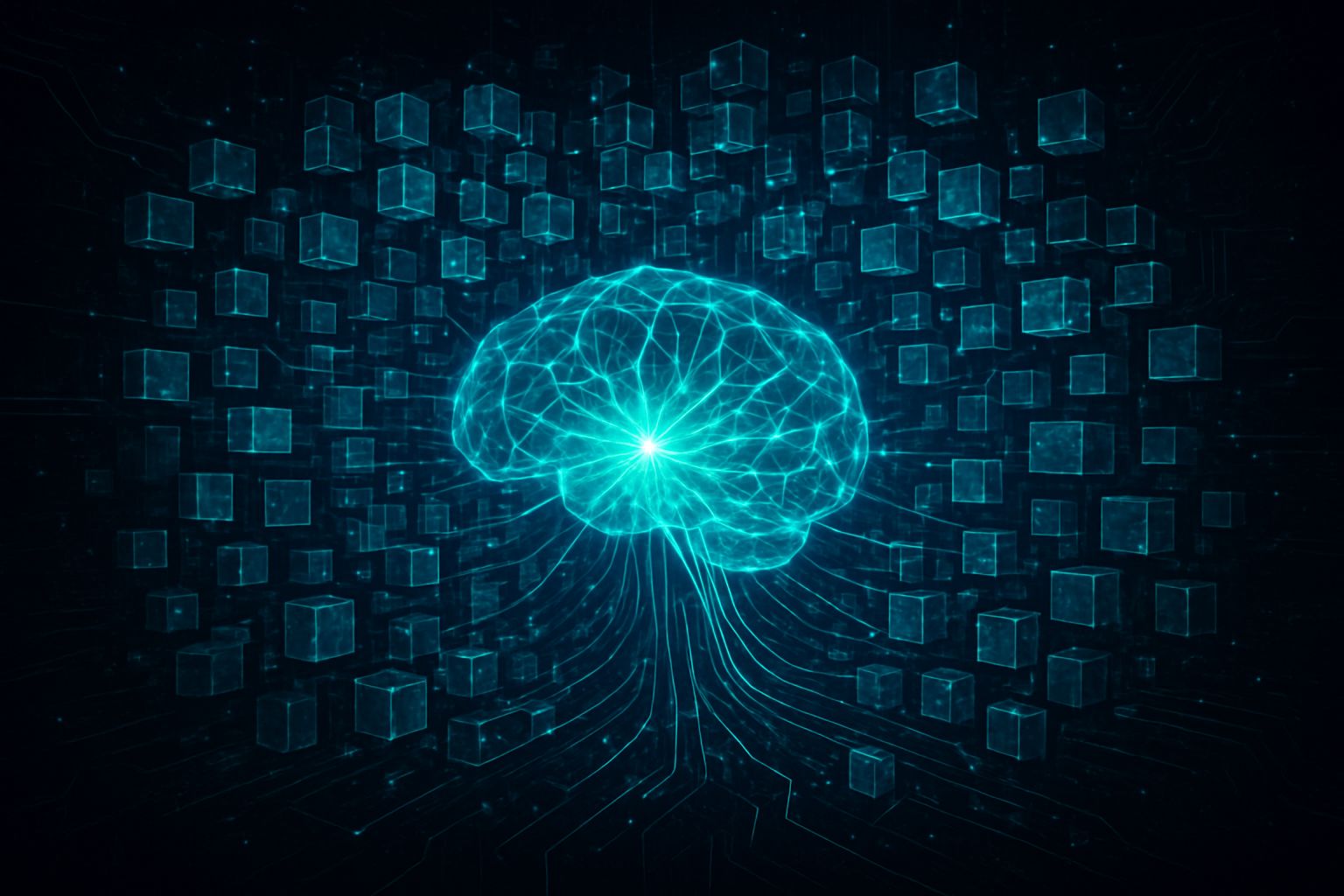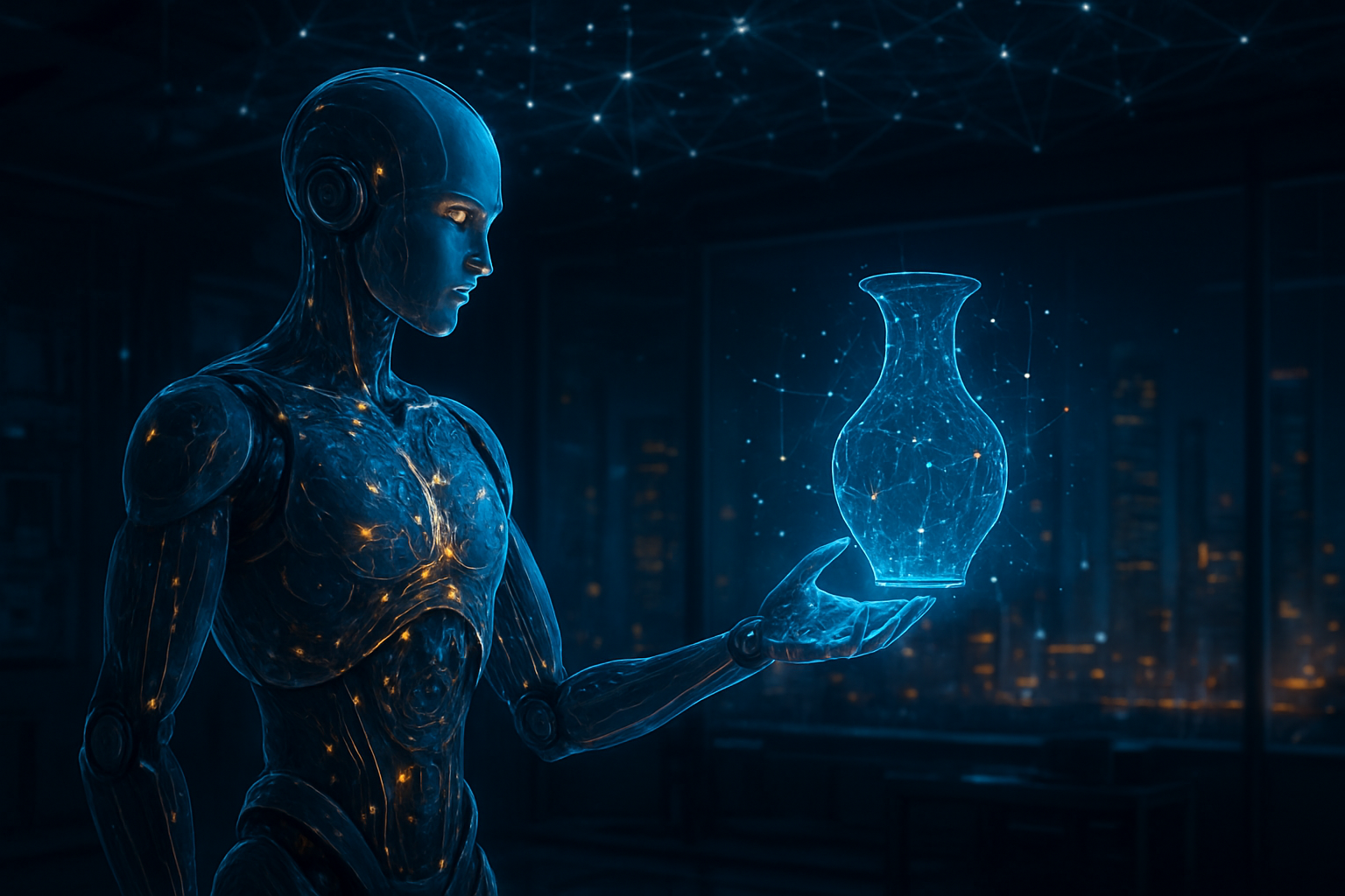
LAS VEGAS — As the tech world gathered for CES 2026, NVIDIA (NASDAQ:NVDA) solidified its transition from a dominant chipmaker to the architect of the "Physical AI" era. The centerpiece of this transformation is NVIDIA Cosmos, a comprehensive platform of World Foundation Models (WFMs) that has fundamentally changed how machines understand, predict, and interact with the physical world. While Large Language Models (LLMs) taught machines to speak, Cosmos is teaching them the laws of physics, causal reasoning, and spatial awareness, effectively providing the "prefrontal cortex" for a new generation of autonomous systems.
The immediate significance of the Cosmos 2.0 announcement lies in its ability to bridge the "sim-to-real" gap that has long plagued the robotics industry. By enabling robots to simulate millions of hours of physical interaction within a digitally imagined environment—before ever moving a mechanical joint—NVIDIA has effectively commoditized complex physical reasoning. This move positions the company not just as a hardware vendor, but as the foundational operating system for every autonomous entity, from humanoid factory workers to self-driving delivery fleets.
The Technical Core: Tokens, Time, and Tensors
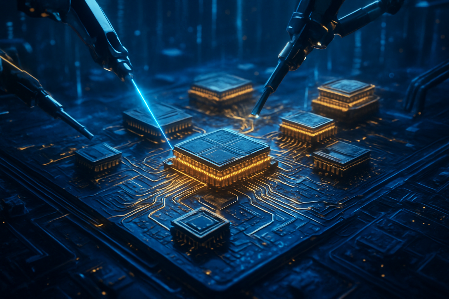
At the heart of the latest update is Cosmos Reason 2, a vision-language-action (VLA) model that has redefined the Physical AI Bench standards. Unlike previous robotic controllers that relied on rigid, pre-programmed heuristics, Cosmos Reason 2 employs a "Chain-of-Thought" planning mechanism for physical tasks. When a robot is told to "clean up a spill," the model doesn't just execute a grab command; it reasons through the physics of the liquid, the absorbency of the cloth, and the sequence of movements required to prevent further spreading. This represents a shift from reactive robotics to proactive, deliberate planning.
Technical specifications for Cosmos 2.5, released alongside the reasoning engine, include a breakthrough visual tokenizer that offers 8x higher compression and 12x faster processing than the industry standards of 2024. This allows the AI to process high-resolution video streams in real-time, "seeing" the world in a way that respects temporal consistency. The platform consists of three primary model tiers: Cosmos Nano, designed for low-latency inference on edge devices; Cosmos Super, the workhorse for general industrial robotics; and Cosmos Ultra, a 14-billion-plus parameter giant used to generate high-fidelity synthetic data.
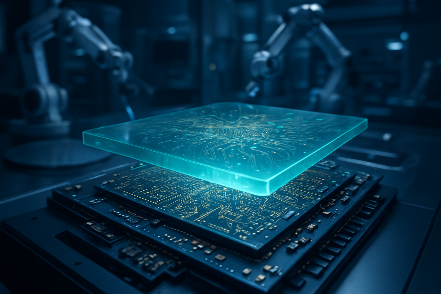
The system's predictive capabilities, housed in Cosmos Predict 2.5, can now forecast up to 30 seconds of physically plausible future states. By "imagining" what will happen if a specific action is taken—such as how a fragile object might react to a certain grip pressure—the AI can refine its movements in a mental simulator before executing them. This differs from previous approaches that relied on massive, real-world trial-and-error, which was often slow, expensive, and physically destructive.
Initial reactions from the AI research community have been largely celebratory, though tempered by the sheer compute requirements. Experts at Stanford and MIT have noted that NVIDIA's tokenizer is the first to truly solve the problem of "object permanence" in AI vision, ensuring that the model understands an object still exists even when it is briefly obscured from view. However, some researchers have raised questions about the "black box" nature of these world models, suggesting that understanding why a model predicts a certain physical outcome remains a significant challenge.
Market Disruption: The Operating System for Robotics
NVIDIA's strategic positioning with Cosmos 2.0 is a direct challenge to the vertical integration strategies of companies like Tesla (NASDAQ:TSLA). While Tesla relies on its proprietary FSD (Full Self-Driving) data and the Dojo supercomputer to train its Optimus humanoid, NVIDIA is providing an "open" alternative for the rest of the industry. Companies like Figure AI and 1X have already integrated Cosmos into their stacks, allowing them to match or exceed the reasoning capabilities of Optimus without needing Tesla’s multi-billion-mile driving dataset.
This development creates a clear divide in the market. On one side are the vertically integrated giants like Tesla, aiming to be the "Apple of Robotics." On the other is the NVIDIA ecosystem, which functions more like Android, providing the underlying intelligence layer for dozens of hardware manufacturers. Major players like Uber (NYSE:UBER) have already leveraged Cosmos to simulate "long-tail" edge cases for their robotaxi services—scenarios like a child chasing a ball into a street—that are too dangerous to test in reality.
The competitive implications are also being felt by traditional AI labs. OpenAI, which recently issued a massive Request for Proposals (RFP) to secure its own robotics supply chain, now finds itself in a "co-opetition" with NVIDIA. While OpenAI provides the high-level cognitive reasoning through its GPT series, NVIDIA's Cosmos is winning the battle for the "low-level" physical intuition required for fine motor skills and spatial navigation. This has forced major venture capital firms, including Goldman Sachs (NYSE:GS), to re-evaluate the valuation of robotics startups based on their "Cosmos-readiness."
For startups, Cosmos represents a massive reduction in the barrier to entry. A small robotics firm no longer needs a massive data collection fleet to train a capable robot; they can instead use Cosmos Ultra to generate high-quality synthetic training data tailored to their specific use case. This shift is expected to trigger a wave of "niche humanoids" designed for specific environments like hospitals, high-security laboratories, and underwater maintenance.
Broader Significance: The World Model Milestone
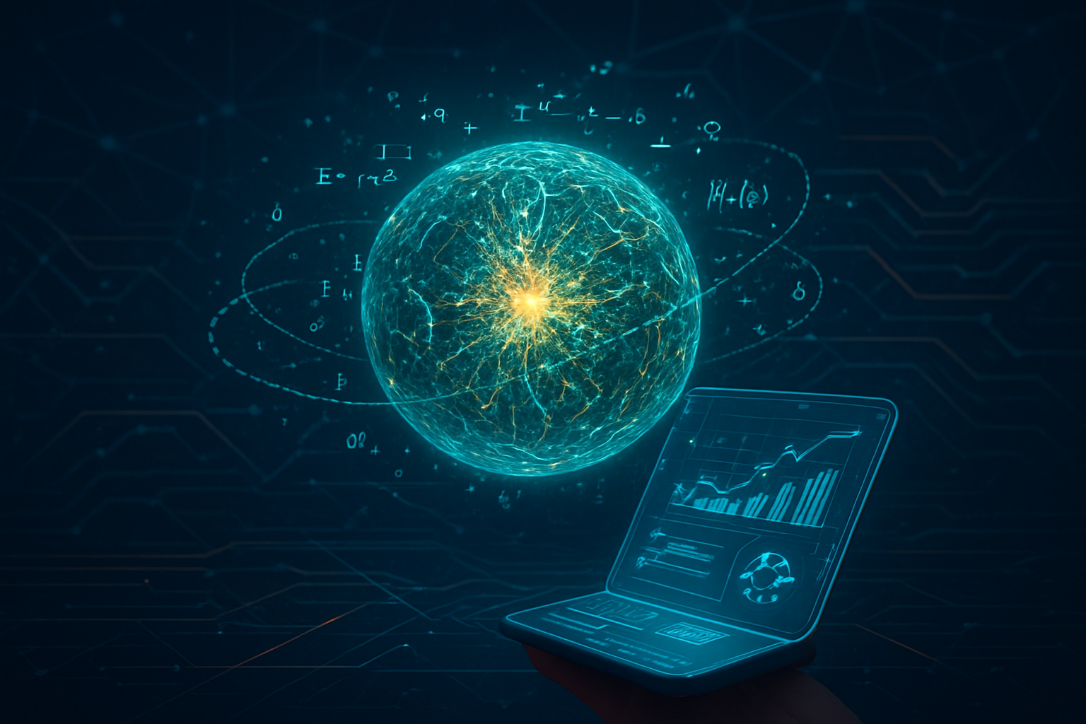
The rise of NVIDIA Cosmos marks a pivot in the broader AI landscape from "Information AI" to "Physical AI." For the past decade, the focus has been on processing text and images—data that exists in a two-dimensional digital realm. Cosmos represents the first successful large-scale effort to codify the three-dimensional, gravity-bound reality we inhabit. It moves AI beyond mere pattern recognition and into the realm of "world modeling," where the machine possesses a functional internal representation of reality.
However, this breakthrough has not been without controversy. In late 2024 and throughout 2025, reports surfaced that NVIDIA had trained Cosmos by scraping millions of hours of video from platforms like YouTube and Netflix. This has led to ongoing legal challenges from content creator collectives who argue that their "human lifetimes of video" were ingested without compensation to teach robots how to move and behave. The outcome of these lawsuits could define the fair-use boundaries for physical AI training for the next decade.
Comparisons are already being drawn between the release of Cosmos and the "ImageNet moment" of 2012 or the "ChatGPT moment" of 2022. Just as those milestones unlocked computer vision and natural language processing, Cosmos is seen as the catalyst that will finally make robots useful in unstructured environments. Unlike a factory arm that moves in a fixed path, a Cosmos-powered robot can navigate a messy kitchen or a crowded construction site because it understands the "why" behind physical interactions, not just the "how."
Future Outlook: From Simulation to Autonomy
Looking ahead, the next 24 months are expected to see a surge in "general-purpose" robotics. With the hardware architectures like NVIDIA’s Rubin (slated for late 2026) providing even more specialized compute for world models, the latency between "thought" and "action" in robots will continue to shrink. Experts predict that by 2027, the cost of a highly capable humanoid powered by the Cosmos stack could drop below $40,000, making them viable for small-scale manufacturing and high-end consumer roles.
The near-term focus will likely be on "multi-modal physical reasoning," where a robot can simultaneously listen to a complex verbal instruction, observe a physical demonstration, and then execute the task in a completely different environment. Challenges remain, particularly in the realm of energy efficiency; running high-parameter world models on a battery-powered humanoid remains a significant engineering hurdle.
Furthermore, the industry is watching closely for the emergence of "federated world models," where robots from different manufacturers could contribute to a shared understanding of physical laws while keeping their specific task-data private. If NVIDIA succeeds in establishing Cosmos as the standard for this data exchange, it will have secured its place as the central nervous system of the 21st-century economy.
A New Chapter in AI History
NVIDIA Cosmos represents more than just a software update; it is a fundamental shift in how artificial intelligence interacts with the human world. By providing a platform that can reason through the complexities of physics and time, NVIDIA has removed the single greatest obstacle to the mass adoption of robotics. The days of robots being confined to safety cages in factories are rapidly coming to an end.
As we move through 2026, the key metric for AI success will no longer be how well a model can write an essay, but how safely and efficiently it can navigate a crowded room or assist in a complex surgery. The significance of this development in AI history cannot be overstated; we have moved from machines that can think about the world to machines that can act within it.
In the coming months, keep a close eye on the deployment of "Cosmos-certified" humanoids in pilot programs across the logistics and healthcare sectors. The success of these trials will determine how quickly the "Physical AI" revolution moves from the lab to our living rooms.
This content is intended for informational purposes only and represents analysis of current AI developments.
TokenRing AI delivers enterprise-grade solutions for multi-agent AI workflow orchestration, AI-powered development tools, and seamless remote collaboration platforms.
For more information, visit https://www.tokenring.ai/.