The traditional role of the television as a passive display has officially come to an end. At CES 2026, Samsung Electronics Co., Ltd. (KRX: 005930) unveiled its most ambitious artificial intelligence project to date: the Vision AI Companion (VAC). Launched under the banner "Your Companion to AI Living," the VAC is a comprehensive software-and-hardware ecosystem that uses real-time computer vision to transform how users interact with their entertainment and their homes. By "seeing" exactly what is on the screen, the VAC can provide contextual suggestions, automate smart home routines, and bridge the gap between digital content and physical reality.
The immediate significance of the VAC lies in its shift toward "agentic" AI—systems that don't just wait for commands but understand the environment and act on behalf of the user. In an era where AI fatigue has begun to set in due to repetitive chatbots, Samsung’s move to integrate vision-based intelligence directly into the television processor represents a major leap forward. It positions the TV not just as an entertainment hub, but as the central nervous system of the modern smart home, capable of identifying products, recognizing human behavior, and orchestrating a fleet of IoT devices with unprecedented precision.
The Technical Core: Beyond Passive Recognition
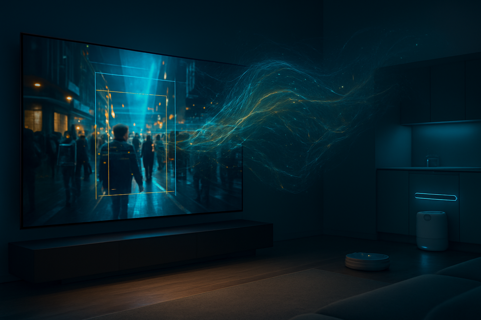
Technically, the Vision AI Companion is a departure from the Automatic Content Recognition (ACR) technologies of the past. While older systems relied on audio fingerprints or metadata tags provided by streaming services, the VAC performs high-speed visual analysis of every frame in real-time. Powering this is the new Micro RGB AI Engine Pro, a custom chipset featuring a dedicated Neural Processing Unit (NPU) capable of handling trillions of operations per second locally. This on-device processing ensures that visual data never leaves the home, addressing the significant privacy concerns that have historically plagued camera-equipped living room devices.
The VAC’s primary capability is its granular object identification. During the keynote demo, Samsung showcased the system identifying specific kitchenware in a cooking show and instantly retrieving the product details for purchase. More impressively, the AI can "extract" information across modalities; if a viewer is watching a travel vlog, the VAC can identify the specific hotel in the background, check flight prices via an integrated Perplexity AI agent, and even coordinate with a Samsung Bespoke AI refrigerator to see if the ingredients for a local dish featured in the show are in stock.
Another standout technical achievement is the "AI Soccer Mode Pro." In this mode, the VAC identifies individual players, ball trajectories, and game situations in real-time. It allows users to manipulate the broadcast audio through the AI Sound Controller Pro, giving them the ability to, for instance, mute specific commentators while boosting the volume of the stadium crowd to simulate a live experience. This level of granular control—enabled by the VAC’s ability to distinguish between different audio-visual elements—surpasses anything previously available in consumer electronics.
Strategic Maneuvers in the AI Arms Race
The launch of the VAC places Samsung in a unique strategic position relative to its competitors. By adopting an "Open AI Agent" approach, Samsung is not trying to compete directly with every AI lab. Instead, the VAC allows users to toggle between Microsoft (NASDAQ: MSFT) Copilot for productivity tasks and Perplexity for web search, while the revamped "Agentic Bixby" handles internal device orchestration. This ecosystem-first approach makes Samsung’s hardware a "must-have" container for the world’s leading AI models, potentially creating a new revenue stream through integrated AI service partnerships.
The competitive implications for other tech giants are stark. While LG Electronics (KRX: 066570) used CES 2026 to focus on "ReliefAI" for healthcare and its Tandem OLED 2.0 panels, Samsung has doubled down on the software-integrated lifestyle. Sony Group Corporation (NYSE: SONY), on the other hand, continues to prioritize "creator intent" and cinematic fidelity, leaving the mass-market AI utility space largely to Samsung. Meanwhile, budget-tier rivals like TCL Technology (SZSE: 000100) and Hisense are finding it increasingly difficult to compete on software ecosystems, even as they narrow the gap in panel specifications like peak brightness and size.
Furthermore, the VAC threatens to disrupt the traditional advertising and e-commerce markets. By integrating "Click to Cart" features directly into the visual stream of a movie or show, Samsung is bypassing the traditional "second screen" (the smartphone) and capturing consumer intent at the moment of inspiration. If successful, this could turn the TV into the world’s most powerful point-of-sale terminal, shifting the balance of power away from traditional retail platforms and toward hardware manufacturers who control the visual interface.
A New Era of Ambient Intelligence
In the broader context of the AI landscape, the Vision AI Companion represents the maturation of ambient intelligence. We are moving away from "The Age of the Prompt," where users must learn how to talk to machines, and into "The Age of the Agent," where machines understand the context of human life. The VAC’s "Home Insights" feature is a prime example: if the TV’s sensors detect a family member falling asleep on the sofa, it doesn't wait for a "Goodnight" command. It proactively dims the lights, adjusts the HVAC, and lowers the volume—a level of seamless integration that has been promised for decades but rarely delivered.
However, this breakthrough does not come without concerns. The primary criticism from the AI research community involves the potential for "AI hallucinations" in product identification and the ethical implications of real-time monitoring. While Samsung has emphasized its "7 years of OS software upgrades" and on-device privacy, the sheer amount of data being processed within the home remains a point of contention. Critics argue that even if data is processed locally, the metadata of a user's life—their habits, their belongings, and their physical presence—could still be leveraged for highly targeted, intrusive marketing.
Comparisons are already being drawn between the VAC and the launch of the first iPhone or the original Amazon Alexa. Like those milestones, the VAC isn't just a new product; it's a new way of interacting with technology. It shifts the TV from a window into another world to a mirror that understands our own. By making the screen "see," Samsung has effectively eliminated the friction between watching and doing, a change that could redefine consumer behavior for the next decade.
The Horizon: From Companion to Household Brain
Looking ahead, the evolution of the Vision AI Companion is expected to move beyond the living room. Industry experts predict that the VAC’s visual intelligence will eventually be decoupled from the TV and integrated into smaller, more mobile devices—including the next generation of Samsung’s "Ballie" rolling robot. In the near term, we can expect "Multi-Room Vision Sync," where the VAC in the living room shares its contextual awareness with the AI in the kitchen, ensuring that the "agentic" experience is consistent throughout the home.
The challenges remaining are significant, particularly in the realm of cross-brand compatibility. While the VAC works seamlessly with Samsung’s SmartThings, the "walled garden" effect could frustrate users with devices from competing ecosystems. For the VAC to truly reach its potential as a universal companion, Samsung will need to lead the way in establishing open standards for vision-based AI communication between different manufacturers. Experts will be watching closely to see if the VAC can maintain its accuracy as more complex, crowded home environments are introduced to the system.
The Final Take: The TV Has Finally Woken Up
Samsung’s Vision AI Companion is more than just a software update; it is a fundamental reimagining of what a display can be. By successfully merging real-time computer vision with a multi-agent AI platform, Samsung has provided a compelling answer to the question of what "AI in the home" actually looks like. The key takeaways from CES 2026 are clear: the era of passive viewing is over, and the era of the proactive, visual agent has begun.
The significance of this development in AI history cannot be overstated. It marks one of the first times that high-level computer vision has been packaged as a consumer-facing utility rather than a security or industrial tool. In the coming weeks and months, the industry will be watching for the first consumer reviews and the rollout of third-party "Vision Apps" that could expand the VAC’s capabilities even further. For now, Samsung has set a high bar, challenging the rest of the tech world to stop talking to their devices and start letting their devices see them.
This content is intended for informational purposes only and represents analysis of current AI developments.
TokenRing AI delivers enterprise-grade solutions for multi-agent AI workflow orchestration, AI-powered development tools, and seamless remote collaboration platforms.
For more information, visit https://www.tokenring.ai/.