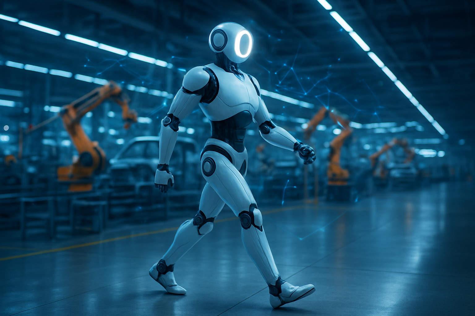
In a move that signals the definitive end of the "viral video" era and the beginning of the industrial humanoid age, Boston Dynamics has officially transitioned its all-electric Atlas robot from the laboratory to the factory floor. As of January 2026, a fleet of the newly unveiled "product-ready" Atlas units has commenced rigorous field tests at the Hyundai Motor Group Metaplant America (HMGMA) (KRX: 005380) in Ellabell, Georgia. This deployment represents one of the first instances of a humanoid robot performing fully autonomous parts sequencing and heavy-lifting tasks in a live automotive manufacturing environment.
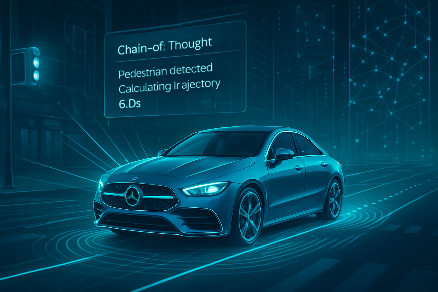
The transition to the Georgia Metaplant is not merely a pilot program; it is the cornerstone of Hyundai’s vision for a "software-defined factory." By integrating Atlas into the $7.6 billion EV and battery facility, Hyundai and Boston Dynamics are attempting to prove that humanoid robots can move beyond scripted acrobatics to handle the unpredictable, high-stakes labor of modern manufacturing. The immediate significance lies in the robot's ability to operate in "fenceless" environments, working alongside human technicians and traditional automation to bridge the gap between fixed-station robotics and manual labor.
The Technical Evolution: From Hydraulics to High-Torque Electric Precision
The 2026 iteration of the electric Atlas, colloquially known within the industry as the "Product Version," is a radical departure from its hydraulic predecessor. Standing at 1.9 meters and weighing 90 kilograms, the robot features a distinctive "baby blue" protective chassis and a ring-lit sensor head designed for 360-degree perception. Unlike human-constrained designs, this Atlas utilizes specialized high-torque actuators and 56 degrees of freedom, including limbs and a torso capable of rotating a full 360 degrees. This "superhuman" range of motion allows the robot to orient its body toward a task without moving its feet, significantly reducing its floor footprint and increasing efficiency in the tight corridors of the Metaplant’s warehouse.
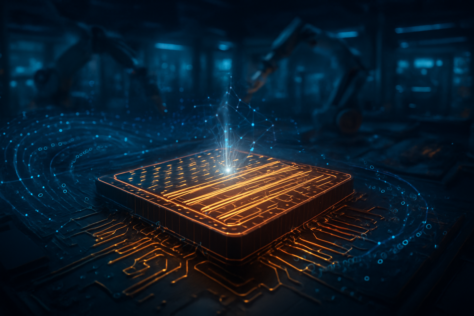
Technical specifications of the deployed units include the integration of the NVIDIA (NASDAQ: NVDA) Jetson Thor compute platform, based on the Blackwell architecture, which provides the massive localized processing power required for real-time spatial AI. For energy management, the electric Atlas has solved the "runtime hurdle" that plagued earlier prototypes. It now features an autonomous dual-battery swapping system, allowing the robot to navigate to a charging station, swap its own depleted battery for a fresh one in under three minutes, and return to work—achieving a near-continuous operational cycle. Initial reactions from the AI research community have been overwhelmingly positive, with experts noting that the robot’s "fenceless" safety rating (IP67 water and dust resistance) and its use of Google DeepMind’s Gemini Robotics models for semantic reasoning represent a massive leap in multi-modal AI integration.
Market Implications: The Humanoid Arms Race
The deployment at HMGMA places Hyundai and Boston Dynamics in a direct technological arms race with other tech titans. Tesla (NASDAQ: TSLA) has been aggressively testing its Optimus Gen 3 robots within its own Gigafactories, focusing on high-volume production and fine-motor tasks like battery cell manipulation. Meanwhile, startups like Figure AI—backed by Microsoft (NASDAQ: MSFT) and OpenAI—have demonstrated significant staying power with their recent long-term deployment at BMW (OTC: BMWYY) facilities. While Tesla’s Optimus aims for a lower price point and mass consumer availability, the Boston Dynamics-Hyundai partnership is positioning Atlas as the "premium" industrial workhorse, capable of handling heavier payloads and more rugged environmental conditions.
For the broader robotics industry, this milestone validates the "Data Factory" business model. To support the Georgia deployment, Hyundai has opened the Robot Metaplant Application Center (RMAC), a facility dedicated to "digital twin" simulations where Atlas robots are trained on virtual versions of the Metaplant floor before ever taking a physical step. This strategic advantage allows for rapid software updates and edge-case troubleshooting without interrupting actual vehicle production. This move essentially disrupts the traditional industrial robotics market, which has historically relied on stationary, single-purpose arms, by offering a versatile asset that can be repurposed across different plant sections as manufacturing needs evolve.
Societal and Global Significance: The End of Labor as We Know It?
The wider significance of the Atlas field tests extends into the global labor landscape and the future of human-robot collaboration. As industrialized nations face worsening labor shortages in manufacturing and logistics, the successful integration of humanoid labor at HMGMA serves as a proof-of-concept for the entire industrial sector. This isn't just about replacing human workers; it's about shifting the human role from "manual mover" to "robot fleet manager." However, this shift does not come without concerns. Labor unions and economic analysts are closely watching the Georgia tests, raising questions about the long-term displacement of entry-level manufacturing roles and the necessity of new regulatory frameworks for autonomous heavy machinery.
In terms of the broader AI landscape, this deployment mirrors the "ChatGPT moment" for physical AI. Just as large language models moved from research papers to everyday tools, the electric Atlas represents the moment humanoid robotics moved from controlled laboratory demos to the messy, unpredictable reality of a 24/7 production line. Compared to previous breakthroughs like the first backflip of the hydraulic Atlas in 2017, the current field tests are less "spectacular" to the casual observer but far more consequential for the global economy, as they demonstrate reliability, durability, and ROI—the three pillars of industrial technology.
The Future Roadmap: Scaling to 30,000 Units
Looking ahead, the road for Atlas at the Georgia Metaplant is structured in multi-year phases. Near-term developments in 2026 will focus on "robot-only" shifts in high-hazard areas, such as areas with high temperatures or volatile chemical exposure, where human presence is currently limited. By 2028, Hyundai plans to transition from "sequencing" (moving parts) to "assembly," where Atlas units will use more advanced end-effectors to install components like trim pieces or weather stripping. Experts predict that the next major challenge will be "fleet-wide emergent behavior"—the ability for dozens of Atlas units to coordinate their movements and share environmental data in real-time without centralized control.
Furthermore, the long-term applications of the Atlas platform are expected to leak into other sectors. Once the "ruggedized" industrial version is perfected, a "service" variant of Atlas could likely emerge for disaster response, nuclear decommissioning, or even large-scale construction. The primary hurdle remains the cost-benefit ratio; while the technical capabilities are proven, the industry is now waiting to see if the cost of maintaining a humanoid fleet can fall below the cost of traditional automation or human labor. Predicative maintenance AI will be the next major software update, allowing Atlas to self-diagnose mechanical wear before a failure occurs on the production line.
A New Chapter in Industrial Robotics
In summary, the arrival of the electric Atlas at the Hyundai Metaplant in Georgia marks a watershed moment for the 21st century. It represents the culmination of decades of research into balance, perception, and power density, finally manifesting as a viable tool for global commerce. The key takeaways from this deployment are clear: the hardware is finally robust enough for the "real world," the AI is finally smart enough to handle "fenceless" environments, and the economic incentive for humanoid labor is no longer a futuristic theory.
As we move through 2026, the industry will be watching the HMGMA's throughput metrics and safety logs with intense scrutiny. The success of these field tests will likely determine the speed at which other automotive giants and logistics firms adopt humanoid solutions. For now, the sight of a faceless, 360-degree rotating robot autonomously sorting car parts in the Georgia heat is no longer science fiction—it is the new standard of the American factory floor.
This content is intended for informational purposes only and represents analysis of current AI developments.
TokenRing AI delivers enterprise-grade solutions for multi-agent AI workflow orchestration, AI-powered development tools, and seamless remote collaboration platforms.
For more information, visit https://www.tokenring.ai/.