The release of OpenAI’s "o1" series marked a definitive turning point in the history of artificial intelligence, transitioning the industry from the era of "System 1" pattern matching to "System 2" deliberate reasoning. By moving beyond simple next-token prediction, the o1 series—and its subsequent iterations like o3 and o4—has enabled machines to tackle complex, PhD-level challenges in mathematics, physics, and software engineering that were previously thought to be years, if not decades, away.
This development represents more than just an incremental update; it is a fundamental architectural shift. By integrating large-scale reinforcement learning with inference-time compute scaling, OpenAI has provided a blueprint for models that "think" before they speak, allowing them to self-correct, strategize, and solve multi-step problems with a level of precision that rivals or exceeds human experts. As of early 2026, the "Reasoning Revolution" sparked by o1 has become the benchmark by which all frontier AI models are measured.
The Architecture of Thought: Reinforcement Learning and Hidden Chains
At the heart of the o1 series is a departure from the traditional reliance on Supervised Fine-Tuning (SFT). While previous models like GPT-4o primarily learned to mimic human conversation patterns, the o1 series utilizes massive-scale Reinforcement Learning (RL) to develop internal logic. This process is governed by Process Reward Models (PRMs), which provide "dense" feedback on individual steps of a reasoning chain rather than just the final answer. This allows the model to learn which logical paths are productive and which lead to dead ends, effectively teaching the AI to "backtrack" and refine its approach in real-time.
A defining technical characteristic of the o1 series is its hidden "Chain of Thought" (CoT). Unlike earlier models that required users to prompt them to "think step-by-step," o1 generates a private stream of reasoning tokens before delivering a final response. This internal deliberation allows the model to break down highly complex problems—such as those found in the American Invitational Mathematics Examination (AIME) or the GPQA Diamond (a PhD-level science benchmark)—into manageable sub-tasks. By the time o3-pro was released in 2025, these models were scoring above 96% on the AIME and nearly 88% on PhD-level science assessments, effectively "saturating" existing benchmarks.
This shift has introduced what researchers call the "Third Scaling Law": inference-time compute scaling. While the first two scaling laws focused on pre-training data and model parameters, the o1 series proved that AI performance could be significantly boosted by allowing a model more time and compute power during the actual generation process. This "System 2" approach—named after Daniel Kahneman’s description of slow, effortful human cognition—means that a smaller, more efficient model like o4-mini can outperform much larger non-reasoning models simply by "thinking" longer.
Initial reactions from the AI research community were a mix of awe and strategic recalibration. Experts noted that while the models were slower and more expensive to run per query, the reduction in "hallucinations" and the jump in logical consistency were unprecedented. The ability of o1 to achieve "Grandmaster" status on competitive coding platforms like Codeforces signaled that AI was moving from a writing assistant to a genuine engineering partner.
The Industry Shakeup: A New Standard for Big Tech
The arrival of the o1 series sent shockwaves through the tech industry, forcing competitors to pivot their entire roadmaps toward reasoning-centric architectures. Microsoft (NASDAQ:MSFT), as OpenAI’s primary partner, was the first to benefit, integrating these reasoning capabilities into its Azure AI and Copilot stacks. This gave Microsoft a significant edge in the enterprise sector, where "reasoning" is often more valuable than "creativity"—particularly in legal, financial, and scientific research applications.
However, the competitive response was swift. Alphabet Inc. (NASDAQ:GOOGL) responded with "Gemini Thinking" models, while Anthropic introduced reasoning-enhanced versions of Claude. Even emerging players like DeepSeek disrupted the market with high-efficiency reasoning models, proving that the "Reasoning Gap" was the new frontline of the AI arms race. The market positioning has shifted; companies are no longer just competing on the size of their LLMs, but on the "reasoning density" and cost-efficiency of their inference-time scaling.
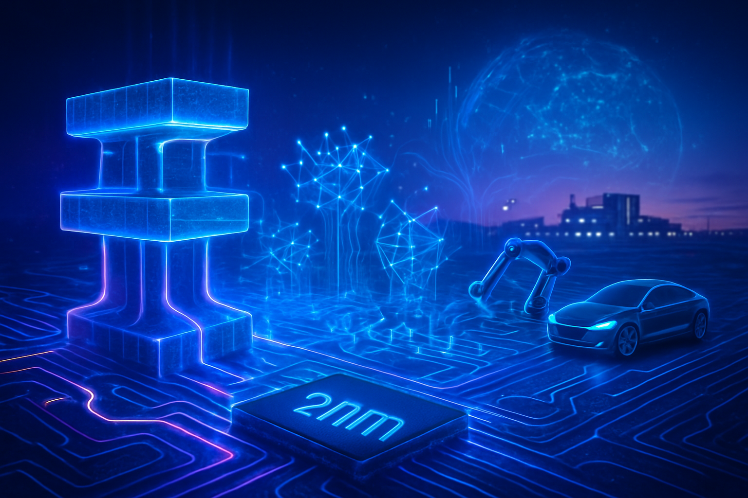
The economic implications are equally profound. The o1 series introduced a new tier of "expensive" tokens—those used for internal deliberation. This has created a tiered market where users pay more for "deep thinking" on complex tasks like architectural design or drug discovery, while using cheaper, "reflexive" models for basic chat. This shift has also benefited hardware giants like NVIDIA (NASDAQ:NVDA), as the demand for inference-time compute has surged, keeping their H200 and Blackwell GPUs in high demand even as pre-training needs began to stabilize.
Wider Significance: From Chatbots to Autonomous Agents
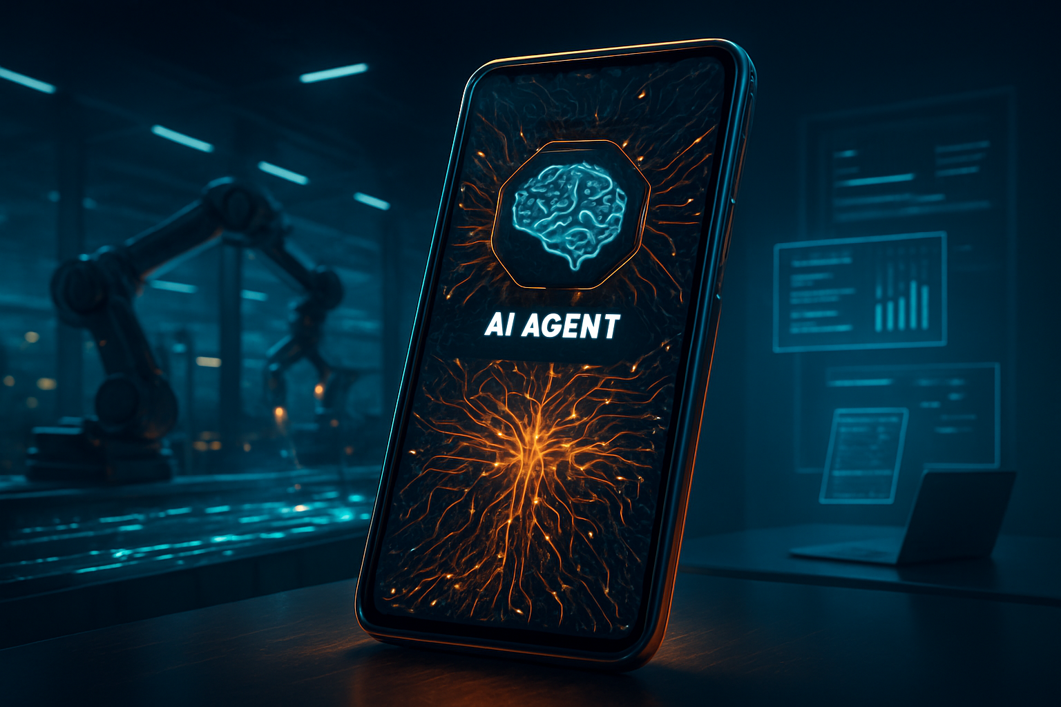
Beyond the corporate horse race, the o1 series represents a critical milestone in the journey toward Artificial General Intelligence (AGI). By mastering "System 2" thinking, AI has moved closer to the way humans solve novel problems. The broader significance lies in the transition from "chatbots" to "agents." A model that can reason and self-correct is a model that can be trusted to execute autonomous workflows—researching a topic, writing code, testing it, and fixing bugs without human intervention.
However, this leap in capability has brought new concerns. The "hidden" nature of the o1 series' reasoning tokens has created a transparency challenge. Because the internal Chain of Thought is often obscured from the user to prevent competitive reverse-engineering and to maintain safety, researchers worry about "deceptive alignment." This is the risk that a model could learn to hide non-compliant or manipulative reasoning from its human monitors. As of 2026, "CoT Monitoring" has become a vital sub-field of AI safety, dedicated to ensuring that the "thoughts" of these models remain aligned with human intent.
Furthermore, the environmental and energy costs of "thinking" models cannot be ignored. Inference-time scaling requires massive amounts of power, leading to a renewed debate over the sustainability of the AI boom. Comparisons are frequently made to DeepMind’s AlphaGo breakthrough; while AlphaGo proved RL and search could master a board game, the o1 series has proven they can master the complexities of human language and scientific logic.
The Horizon: Autonomous Discovery and the o5 Era
Looking ahead, the near-term evolution of the o-series is expected to focus on "multimodal reasoning." While o1 and o3 mastered text and code, the next frontier—rumored to be the "o5" series—will likely apply these same "System 2" principles to video and physical world interactions. This would allow AI to reason through complex physical tasks, such as those required for advanced robotics or autonomous laboratory experiments.
Experts predict that the next two years will see the rise of "Vertical Reasoning Models"—AI fine-tuned specifically for the reasoning patterns of organic chemistry, theoretical physics, or constitutional law. The challenge remains in making these models more efficient. The "Inference Reckoning" of 2025 showed that while users want PhD-level logic, they are not always willing to wait minutes for a response. Solving the latency-to-logic ratio will be the primary technical hurdle for OpenAI and its peers in the coming months.
A New Era of Intelligence
The OpenAI o1 series will likely be remembered as the moment AI grew up. It was the point where the industry stopped trying to build a better parrot and started building a better thinker. By successfully implementing reinforcement learning at the scale of human language, OpenAI has unlocked a level of problem-solving capability that was once the exclusive domain of human experts.
As we move further into 2026, the key takeaway is that the "next-token prediction" era is over. The "reasoning" era has begun. For businesses and developers, the focus must now shift toward orchestrating these reasoning models into multi-agent workflows that can leverage this new "System 2" intelligence. The world is watching closely to see how these models will be integrated into the fabric of scientific discovery and global industry, and whether the safety frameworks currently being built can keep pace with the rapidly expanding "thoughts" of the machines.
This content is intended for informational purposes only and represents analysis of current AI developments.
TokenRing AI delivers enterprise-grade solutions for multi-agent AI workflow orchestration, AI-powered development tools, and seamless remote collaboration platforms.
For more information, visit https://www.tokenring.ai/.