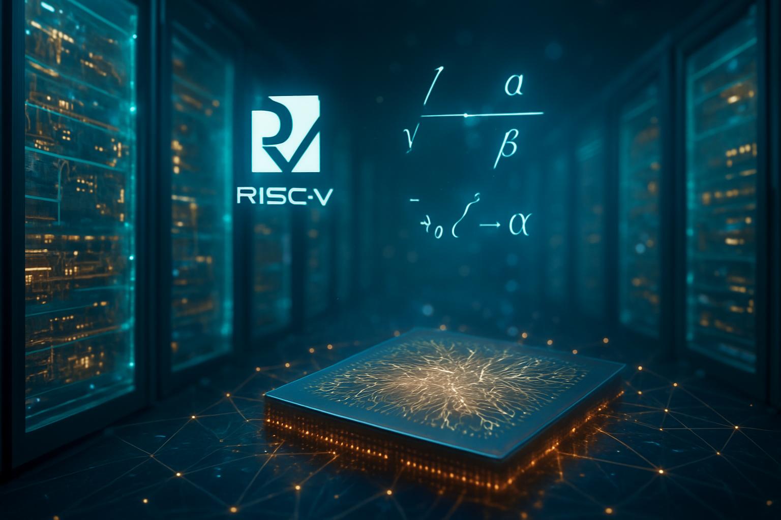
The landscape of data center computing is undergoing its most significant architectural shift in decades. As of early 2026, the RISC-V open-source instruction set architecture (ISA) has officially graduated from its origins in embedded systems to become a formidable "third pillar" in the high-performance computing (HPC) and artificial intelligence markets. By providing a royalty-free, highly customizable alternative to the proprietary models of ARM and Intel (NASDAQ:INTC), RISC-V is enabling a new era of "silicon sovereignty" for hyperscalers and AI chip designers who are eager to bypass the restrictive licensing fees and "black box" designs of traditional vendors.
The immediate significance of this development lies in the rapid maturation of server-grade RISC-V silicon. With the recent commercial availability of high-performance cores like Tenstorrent’s Ascalon and the strategic acquisition of Ventana Micro Systems by Qualcomm (NASDAQ:QCOM) in late 2025, the industry has signaled that RISC-V is no longer just a theoretical threat. It is now a primary contender for the massive AI inference and training workloads that define the modern data center, offering a level of architectural flexibility that neither x86 nor ARM can easily match in their current forms.
Technical Breakthroughs: Vector Agnosticism and Chiplet Modularity
The technical prowess of RISC-V in 2026 is anchored by the implementation of the RISC-V Vector (RVV) 1.0 extensions. Unlike the fixed-width SIMD (Single Instruction, Multiple Data) approaches found in Intel’s AVX-512 or ARM’s traditional NEON, RVV utilizes a vector-length agnostic (VLA) model. This allows software written for a 128-bit vector engine to run seamlessly on hardware with 512-bit or even 1024-bit vectors without the need for recompilation. For AI developers, this means a single software stack can scale across a diverse range of hardware, from edge devices to massive AI accelerators, significantly reducing the engineering overhead associated with hardware fragmentation.
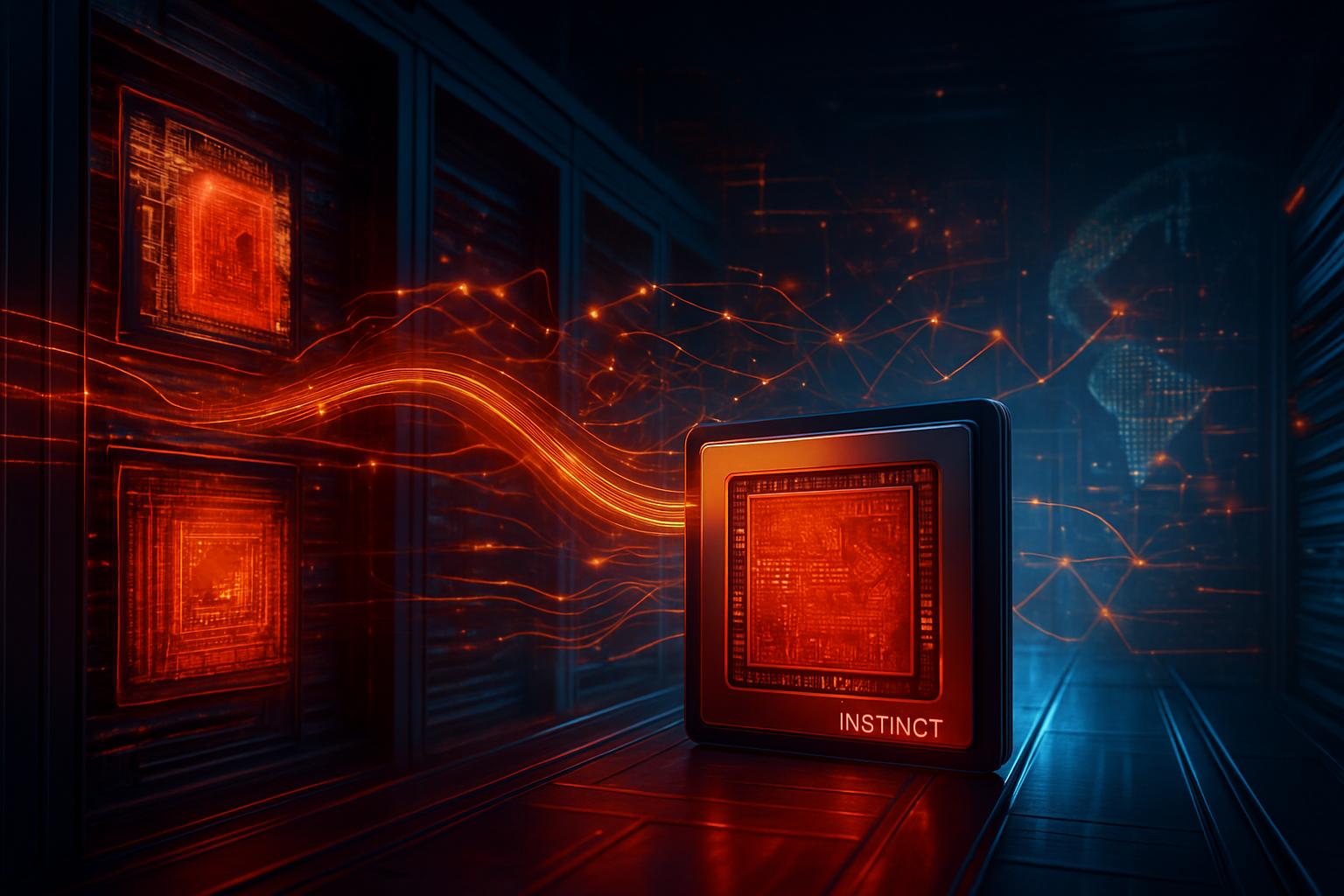
Leading the charge in raw performance is Tenstorrent’s Ascalon-X, an 8-wide decode, out-of-order superscalar core designed under the leadership of industry veteran Jim Keller. Benchmarks released in late 2025 show the Ascalon-X achieving approximately 22 SPECint2006/GHz, placing it in direct competition with the highest-tier cores from AMD (NASDAQ:AMD) and ARM. This performance is achieved through a modular chiplet architecture using the Universal Chiplet Interconnect Express (UCIe) standard, allowing designers to mix and match RISC-V cores with specialized AI accelerators and high-bandwidth memory (HBM) on a single package.
Furthermore, the emergence of the RVA23 profile has standardized the features required for server-class operating systems, ensuring that Linux distributions and containerized workloads run with the same stability as they do on legacy architectures. Initial reactions from the AI research community have been overwhelmingly positive, particularly regarding the ability to add "custom instructions" to the ISA. This allows companies to bake proprietary AI mathematical kernels directly into the silicon, optimizing for specific Transformer-based models or emerging neural network architectures in ways that are physically impossible with the rigid instruction sets of x86 or ARM.
Market Disruption: The End of the "ARM Tax"
The expansion of RISC-V into the data center has sent shockwaves through the semiconductor industry, most notably affecting the strategic positioning of ARM. For years, hyperscalers like Amazon (NASDAQ:AMZN) and Alphabet (NASDAQ:GOOGL) have used ARM-based designs to reduce their reliance on Intel, but they remained tethered to ARM’s licensing fees and roadmap. The shift toward RISC-V represents a "declaration of independence" from these costs. Meta (NASDAQ:META) has already fully integrated RISC-V cores into its MTIA (Meta Training and Inference Accelerator) v3, using them for critical scalar and control tasks to optimize their massive social media recommendation engines.
Qualcomm’s acquisition of Ventana Micro Systems in December 2025 is perhaps the clearest indicator of this market shift. By owning the high-performance RISC-V IP developed by Ventana, Qualcomm is positioning itself to offer cloud-scale server processors that are entirely free from ARM’s royalty structure. This move not only threatens ARM’s revenue streams but also forces a defensive consolidation among legacy players. In response, Intel and AMD formed a landmark "x86 Alliance" in late 2024 to standardize their own architectures, yet they struggle to match the rapid, community-driven innovation cycle that the open-source RISC-V ecosystem provides.
Startups and regional players are also major beneficiaries. In China, Alibaba (NYSE:BABA) has utilized its T-Head semiconductor division to produce the XuanTie C930, a server-grade processor designed to circumvent Western export restrictions on high-end proprietary cores. By leveraging an open ISA, these companies can achieve "silicon sovereignty," ensuring that their national infrastructure is not dependent on the intellectual property of a single foreign corporation. This geopolitical advantage is driving a 60.9% compound annual growth rate (CAGR) for RISC-V in the data center, far outpacing the growth of its rivals.
The Broader AI Landscape: A "Linux Moment" for Hardware
The rise of RISC-V is often compared to the "Linux moment" for hardware. Just as open-source software democratized the server operating system market, RISC-V is democratizing the processor. This fits into the broader AI trend of moving away from general-purpose CPUs toward Domain-Specific Accelerators (DSAs). In an era where AI models are growing exponentially, the "one-size-fits-all" approach of x86 is becoming an energy-efficiency liability. RISC-V’s modularity allows for the creation of lean, highly specialized chips that do exactly what an AI workload requires and nothing more, leading to massive improvements in performance-per-watt.
However, this shift is not without its concerns. The primary challenge remains software fragmentation. While the RISC-V Software Ecosystem (RISE) project—backed by Google, NVIDIA (NASDAQ:NVDA), and Samsung (KRX:005930)—has made enormous strides in porting compilers, libraries, and frameworks like PyTorch and TensorFlow, the "long tail" of enterprise legacy software still resides firmly on x86. Critics also point out that the open nature of the ISA could lead to a proliferation of incompatible "forks" if the community does not strictly adhere to the standards set by RISC-V International.
Despite these hurdles, the comparison to previous milestones like the introduction of the first 64-bit processors is apt. RISC-V represents a fundamental change in how the industry thinks about compute. It is moving the value proposition away from the instruction set itself and toward the implementation and the surrounding ecosystem. This allows for a more competitive and innovative market where the best silicon design wins, rather than the one with the most entrenched licensing moat.
Future Outlook: The Road to 2027 and Beyond
Looking toward 2026 and 2027, the industry expects to see the first wave of "RISC-V native" supercomputers. These systems will likely utilize massive arrays of vector-optimized cores to handle the next generation of multimodal AI models. We are also on the verge of seeing RISC-V integrated into more complex "System-on-a-Chip" (SoC) designs for autonomous vehicles and robotics, where the same power-efficient AI inference capabilities used in the data center can be applied to real-time edge processing.
The near-term challenges will focus on the maturation of the "northbound" software stack—ensuring that high-level orchestration tools like Kubernetes and virtualization layers work flawlessly with RISC-V’s unique vector extensions. Experts predict that by 2028, RISC-V will not just be a "companion" core in AI accelerators but will serve as the primary host CPU for a significant portion of new cloud deployments. The momentum is currently unstoppable, fueled by a global desire for open standards and the relentless demand for more efficient AI compute.
Conclusion: A New Era of Open Compute
The expansion of RISC-V into the data center marks a historic turning point in the evolution of artificial intelligence infrastructure. By breaking the x86-ARM duopoly, RISC-V has provided the industry with a path toward lower costs, greater customization, and true technological independence. The success of high-performance cores like the Ascalon-X and the strategic pivots by giants like Qualcomm and Meta demonstrate that the open-source hardware model is not only viable but essential for the future of hyperscale computing.
In the coming weeks and months, industry watchers should keep a close eye on the first benchmarks of Qualcomm’s integrated Ventana designs and the progress of the RISE project’s software optimization efforts. As more enterprises begin to pilot RISC-V based instances in the cloud, the "third pillar" will continue to solidify its position. The long-term impact will be a more diverse, competitive, and innovative semiconductor landscape, ensuring that the hardware of tomorrow is as open and adaptable as the AI software it powers.
This content is intended for informational purposes only and represents analysis of current AI developments.
TokenRing AI delivers enterprise-grade solutions for multi-agent AI workflow orchestration, AI-powered development tools, and seamless remote collaboration platforms.
For more information, visit https://www.tokenring.ai/.