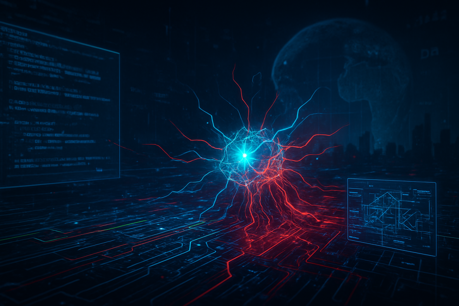
In a bold move that underscores the high-stakes nature of the global AI arms race, NVIDIA (NASDAQ: NVDA) has launched a high-risk, high-reward strategy to reclaim its dominance in the Chinese market. As of early January 2026, the Silicon Valley giant is aggressively pushing its H200 Tensor Core GPU to Chinese tech titans, including ByteDance and Alibaba (NYSE: BABA), under a complex and newly minted regulatory framework. This strategy represents a significant pivot from the "nerfed" hardware of previous years, as NVIDIA now seeks to ship full-spec high-performance silicon while navigating a gauntlet of U.S. export licenses and a mandatory 25% revenue-sharing fee paid directly to the U.S. Treasury.
The immediate significance of this development cannot be overstated. After seeing its market share in China plummet from near-total dominance to negligible levels in 2024 due to strict export controls, NVIDIA’s re-entry with the H200 marks a pivotal moment for the company’s fiscal 2027 outlook. With Chinese "hyperscalers" desperate for the compute power necessary to train frontier-level large language models (LLMs), NVIDIA is betting that its superior architecture can overcome both Washington's rigorous case-by-case reviews and Beijing’s own domestic "matchmaking" policies, which favor local champions like Huawei.
Technical Superiority and the End of "Nerfed" Silicon
The H200 GPU at the center of this strategy is a significant departure from the downgraded "H20" models NVIDIA previously offered to comply with 2023-era restrictions. Based on the Hopper architecture, the H200 being shipped to China in 2026 is a "full-spec" powerhouse, featuring 141GB of HBM3e memory and nearly double the memory bandwidth of its predecessor, the H100. This makes it approximately six times more powerful for AI inference and training than the China-specific chips of the previous year. By offering the standard H200 rather than a compromised version, NVIDIA is providing Chinese firms with the hardware parity they need to compete with Western AI labs, albeit at a steep financial and regulatory cost.
The shift back to high-performance silicon is a calculated response to the limitations of previous "China-spec" chips. Industry experts noted that the downgraded H20 chips were often insufficient for training the massive, trillion-parameter models that ByteDance and Alibaba are currently developing. The H200’s massive memory capacity allows for larger batch sizes and more efficient distributed training across GPU clusters. While NVIDIA’s newer Blackwell and Vera Rubin architectures remain largely off-limits or restricted to even tighter quotas, the H200 has emerged as the "Goldilocks" solution—powerful enough to be useful, but established enough to fit within the U.S. government's new "managed export" framework.
Initial reactions from the AI research community suggest that the H200’s arrival in China could significantly accelerate the development of domestic Chinese LLMs. However, the technical specifications come with a catch: the U.S. Department of Commerce has implemented a rigorous "security inspection" protocol. Every batch of H200s destined for China must undergo a physical and software-level audit in the U.S. to ensure the hardware is not being diverted to military or state-owned research entities. This unprecedented level of oversight ensures that while the hardware is high-spec, its destination is strictly controlled.
Market Dominance vs. Geopolitical Risk: The Corporate Impact
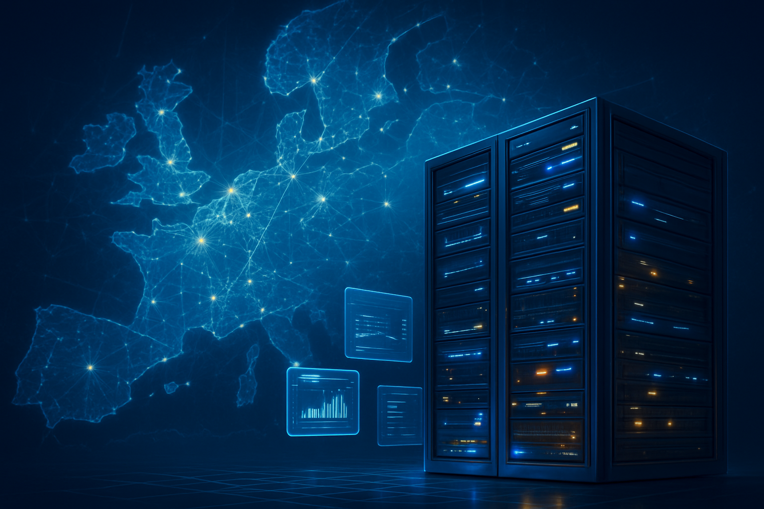
The corporate implications of NVIDIA’s China strategy are immense, particularly for major Chinese tech giants. ByteDance and Alibaba have reportedly placed massive orders, with each company seeking over 200,000 H200 units for 2026 delivery. ByteDance alone is estimated to be spending upwards of $14 billion (approximately 100 billion yuan) on NVIDIA hardware this year. To manage the extreme geopolitical volatility, NVIDIA has implemented a "pay-to-play" model that is virtually unheard of in the industry: Chinese buyers must pay 100% of the order value upfront. These orders are non-cancellable and non-refundable, effectively shifting all risk of a sudden U.S. policy reversal onto the Chinese customers.
This aggressive positioning is a direct challenge to domestic Chinese chipmakers, most notably Huawei and its Ascend 910C series. While Beijing has encouraged its tech giants to "buy local," the sheer performance gap and the maturity of NVIDIA’s CUDA software ecosystem remain powerful draws for Alibaba and Tencent (HKG: 0700). However, the Chinese government has responded with its own "matchmaking" policy, which reportedly requires domestic firms to purchase a specific ratio of Chinese-made chips for every NVIDIA GPU they import. This creates a dual-supply chain reality where Chinese firms must integrate both NVIDIA and Huawei hardware into their data centers.
For NVIDIA, the success of this strategy is critical for its long-term valuation. Analysts estimate that China could contribute as much as $40 billion in revenue in 2026 if the H200 rollout proceeds as planned. This would represent a massive recovery for the company's China business. However, the 25% revenue-sharing fee mandated by the U.S. government adds a significant cost layer. This "tax" on high-end AI exports is a novel regulatory tool designed to allow American companies to profit from the Chinese market while ensuring the U.S. government receives a direct financial benefit that can be reinvested into domestic semiconductor initiatives, such as those funded by the CHIPS Act.
The Broader AI Landscape: A New Era of Managed Trade
NVIDIA’s H200 strategy fits into a broader global trend of "managed trade" in the AI sector. The era of open, unrestricted global semiconductor markets has been replaced by a system of case-by-case reviews and inter-agency oversight involving the U.S. Departments of Commerce, State, Energy, and Defense. This new reality reflects a delicate balance: the U.S. wants to maintain its technological lead and restrict China’s military AI capabilities, but it also recognizes the economic necessity of allowing its leading tech companies to access one of the world’s largest markets.
The 25% revenue-sharing fee is perhaps the most controversial aspect of this new landscape. It sets a precedent where the U.S. government acts as a "silent partner" in high-tech exports to strategic competitors. Critics argue this could lead to higher costs for AI development globally, while proponents see it as a necessary compromise that prevents a total decoupling of the U.S. and Chinese tech sectors. Comparisons are already being made to the Cold War-era COCOM regulations, but with a modern, data-driven twist that focuses on compute power and "frontier" AI capabilities rather than just raw hardware specs.
Potential concerns remain regarding the "leakage" of AI capabilities. Despite the rigorous inspections, some hawks in Washington worry that the sheer volume of H200s entering China—estimated to exceed 2 million units in 2026—will inevitably benefit the Chinese state's strategic goals. Conversely, in Beijing, there is growing anxiety about "NVIDIA dependency." The Chinese government’s push for self-reliance is at an all-time high, and the H200 strategy may inadvertently accelerate China's efforts to build a completely independent semiconductor supply chain, free from U.S. licensing requirements and revenue-sharing taxes.
Future Horizons: Beyond the H200
Looking ahead, the H200 is likely just the first step in a multi-year cycle of high-stakes exports. As NVIDIA ramps up production of its Blackwell (B200) and upcoming Vera Rubin architectures, the cycle of licensing and review will begin anew. Experts predict that NVIDIA will continue to "fire up" its supply chain, with TSMC (NYSE: TSM) playing a critical role in meeting the massive backlog of orders. The near-term focus will be on whether NVIDIA can actually deliver the 2 million units demanded by the Chinese market, given the complexities of the U.S. inspection process and the potential for supply chain bottlenecks.
In the long term, the challenge will be the "moving goalpost" of AI regulation. As AI models become more efficient, the definition of what constitutes a "frontier model" or a "restricted capability" will evolve. NVIDIA will need to continuously innovate not just in hardware, but in its regulatory compliance and risk management strategies. We may see the development of "trusted execution environments" or hardware-level "kill switches" that allow the U.S. to remotely disable chips if they are found to be used for prohibited purposes—a concept that was once science fiction but is now being discussed in the halls of the Department of Commerce.
The next few months will be a litmus test for this strategy. If ByteDance and Alibaba successfully integrate hundreds of thousands of H200s without triggering a new round of bans, it could signal a period of "competitive stability" in U.S.-China tech relations. However, any sign that these chips are being used for military simulations or state surveillance could lead to an immediate and total shutdown of the H200 pipeline, leaving NVIDIA and its Chinese customers in a multi-billion dollar lurch.
A High-Wire Act for the AI Age
NVIDIA’s H200 strategy in China is a masterclass in navigating the intersection of technology, finance, and global politics. By moving away from downgraded hardware and embracing a high-performance, highly regulated export model, NVIDIA is attempting to have it both ways: satisfying the insatiable hunger of the Chinese market while remaining strictly within the evolving boundaries of U.S. national security policy. The 100% upfront payment terms and the 25% U.S. Treasury fee are the price of admission for this high-stakes gambit.
As we move further into 2026, the success of this development will be measured not just in NVIDIA's quarterly earnings, but in the relative pace of AI advancement in Beijing versus Silicon Valley. This is more than just a corporate expansion; it is a real-time experiment in how the world's two superpowers will share—and restrict—the most transformative technology of the 21st century.
Investors and industry watchers should keep a close eye on the upcoming Q1 2026 earnings reports from NVIDIA and Alibaba, as well as any policy updates from the U.S. Bureau of Industry and Security (BIS). The "China Gambit" has begun, and the results will define the AI landscape for years to come.
This content is intended for informational purposes only and represents analysis of current AI developments.
TokenRing AI delivers enterprise-grade solutions for multi-agent AI workflow orchestration, AI-powered development tools, and seamless remote collaboration platforms.
For more information, visit https://www.tokenring.ai/.