Author: mdierolf

  • Silicon Sovereignty: How RISC-V’s Open-Source Revolution is Dismantling the ARM and x86 Duopoly

    Silicon Sovereignty: How RISC-V’s Open-Source Revolution is Dismantling the ARM and x86 Duopoly

    The global semiconductor landscape is undergoing its most significant architectural shift in decades as RISC-V, the open-source instruction set architecture (ISA), officially transitions from an academic curiosity to a mainstream powerhouse. As of early 2026, RISC-V has claimed a staggering 25% market penetration, establishing itself as the "third pillar" of computing alongside the long-dominant x86 and ARM architectures. This surge is driven by a collective industry push toward "silicon sovereignty," where tech giants and startups alike are abandoning restrictive licensing fees in favor of the ability to design custom, purpose-built processors optimized for the age of generative AI.

    The immediate significance of this movement cannot be overstated. By providing a royalty-free, extensible framework, RISC-V is effectively democratizing high-performance computing. Major players are no longer forced to choose between the proprietary constraints of ARM Holdings (NASDAQ: ARM) or the closed ecosystems of Intel (NASDAQ: INTC) and Advanced Micro Devices (NASDAQ: AMD). Instead, the industry is witnessing a localized manufacturing and design boom, as companies leverage RISC-V to create specialized hardware for everything from ultra-efficient wearables to massive AI training clusters in the data center.

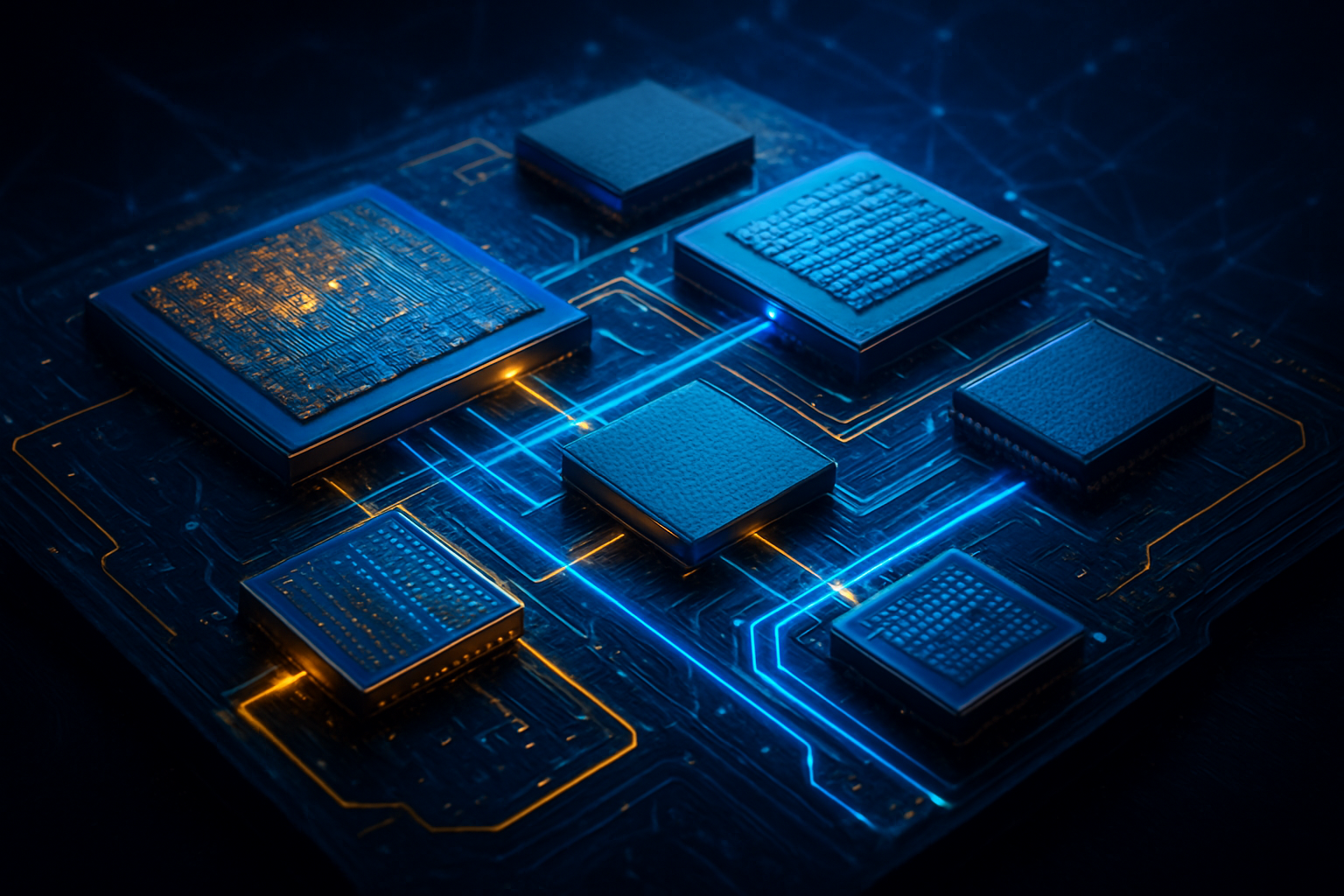
    The technical maturation of RISC-V in the last 24 months has been nothing short of transformative. In late 2025, the ratification of the RVA23 Profile served as a "stabilization event" for the entire ecosystem, providing a mandatory set of ISA extensions—including advanced vector operations and atomic instructions—that ensure software portability across different hardware vendors. This standardization has allowed high-performance cores like the SiFive Performance P870-D and the Ventana Veyron V2 to reach performance parity with top-tier ARM Neoverse and x86 server chips. The Veyron V2, for instance, now supports up to 192 cores per system, specifically targeting the high-throughput demands of modern cloud infrastructures.

    Unlike the rigid "black box" approach of x86 or the tiered licensing of ARM, RISC-V’s modularity allows engineers to add custom instructions directly into the processor. This capability is particularly vital for AI workloads, where standard general-purpose instructions often create bottlenecks. New releases, such as the SiFive 2nd Gen Intelligence (XM Series) slated for mid-2026, feature 1,024-bit vector lengths designed specifically to accelerate transformer-based models. This level of customization allows developers to strip away unnecessary silicon "bloat," reducing power consumption and increasing compute density in ways that were previously impossible under proprietary models.

    Initial reactions from the AI research community have been overwhelmingly positive, with experts noting that RISC-V’s open nature aligns perfectly with the open-source software movement. By having full visibility into the hardware's execution pipeline, researchers can optimize compilers and kernels with surgical precision. Industry analysts at the SHD Group suggest that the ability to "own the architecture" is the primary driver for this shift, as it removes the existential risk of a licensing partner changing terms or being acquired by a competitor.

    The competitive implications of RISC-V’s ascent are reshaping the strategic roadmaps of every major tech firm. In a landmark move in December 2025, Qualcomm (NASDAQ: QCOM) acquired Ventana Micro Systems, a leader in high-performance RISC-V CPUs. This acquisition signals a clear "second path" for Qualcomm, allowing them to integrate high-performance RISC-V cores into their Snapdragon and Oryon roadmaps, effectively gaining leverage in their ongoing licensing disputes with ARM. Similarly, Meta Platforms (NASDAQ: META) has fully embraced the architecture for its MTIA (Meta Training and Inference Accelerator) chips, utilizing RISC-V cores from Andes Technology to slash its annual compute bill and reduce its dependency on high-margin AI hardware from NVIDIA (NASDAQ: NVDA).

    Alphabet Inc. (NASDAQ: GOOGL), through its Google division, has also become a cornerstone of the RISC-V Software Ecosystem (RISE) consortium. Google’s commitment to making RISC-V a "Tier-1" architecture for Android has paved the way for the first commercial RISC-V smartphones, expected to debut in late 2026. For tech giants, the strategic advantage is clear: by moving to an open architecture, they can divert billions of dollars previously earmarked for royalties into R&D for custom silicon that provides a unique competitive edge in AI performance.

    Startups are also finding a lower barrier to entry in the hardware space. Without the multi-million dollar "upfront" licensing fees required by proprietary ISAs, a new generation of "fabless" AI startups is emerging. These companies are building niche accelerators for edge computing and autonomous systems, often reaching market faster than traditional competitors. This disruption is forcing established incumbents like Intel to pivot; Intel’s Foundry Services (IFS) has notably begun offering RISC-V manufacturing services to capture the growing demand from customers who are designing their own open-source chips.

    The broader significance of the RISC-V push lies in its role as a geopolitical and economic stabilizer. In an era of increasing trade restrictions and "chip wars," RISC-V offers a neutral ground. Alibaba Group (NYSE: BABA) has been a primary beneficiary of this, with its XuanTie C930 processors proving that high-end server performance can be achieved without relying on Western-controlled proprietary IP. This shift toward "semiconductor sovereignty" allows nations to build their own domestic tech industries on a foundation that cannot be revoked by a single corporate entity or foreign government.

    However, this transition is not without concerns. The fragmentation of the ecosystem remains a potential pitfall; if too many companies implement highly specialized custom instructions without adhering to the RVA23 standards, the "write once, run anywhere" promise of modern software could be jeopardized. Furthermore, security researchers have pointed out that while open-source architecture allows for more "eyes on the code," it also means that vulnerabilities in the base ISA could be exploited across a wider range of devices if not properly audited.

    Comparatively, the rise of RISC-V is being likened to the "linux moment" for hardware. Just as Linux broke the monopoly of proprietary operating systems in the data center, RISC-V is doing the same for the silicon layer. This milestone represents a shift from a world where hardware dictated software capabilities to one where software requirements—specifically the massive demands of LLMs and generative AI—dictate the hardware design.

    Looking ahead, the next 18 to 24 months will be defined by the arrival of RISC-V in the consumer mainstream. While the architecture has already conquered the embedded and microcontroller markets, the launch of the first high-end RISC-V laptops and flagship smartphones in late 2026 will be the ultimate litmus test. Experts predict that the automotive sector will be the next major frontier, with the Quintauris consortium—backed by giants like NXP Semiconductors (NASDAQ: NXPI) and Robert Bosch GmbH—expected to ship standardized RISC-V platforms for autonomous driving by early 2027.

    The primary challenge remains the "last mile" of software optimization. While major languages like Python, Rust, and Java now have mature RISC-V runtimes, highly optimized libraries for specialized AI tasks are still being ported. The industry is watching closely to see if the RISE consortium can maintain its momentum and prevent the kind of fragmentation that plagued early Unix distributions. If successful, the long-term result will be a more diverse, resilient, and cost-effective global computing infrastructure.

    The mainstream push of RISC-V marks the end of the "black box" era of computing. By providing a license-free, high-performance alternative to ARM and x86, RISC-V has empowered a new wave of innovation centered on customization and efficiency. The key takeaways are clear: the architecture is no longer a secondary option but a primary strategic choice for the world’s largest tech companies, driven by the need for specialized AI hardware and geopolitical independence.

    In the history of artificial intelligence and computing, 2026 will likely be remembered as the year the silicon gatekeepers lost their grip. As we move into the coming months, the industry will be watching for the first consumer device benchmarks and the continued integration of RISC-V into hyperscale data centers. The open-source revolution has reached the motherboard, and the implications for the future of AI are profound.


    This content is intended for informational purposes only and represents analysis of current AI developments.

    TokenRing AI delivers enterprise-grade solutions for multi-agent AI workflow orchestration, AI-powered development tools, and seamless remote collaboration platforms.
    For more information, visit https://www.tokenring.ai/.

  • The Electric Nerve System: How Silicon Carbide and AI Are Rewriting the Rules of EV Range and Charging

    The Electric Nerve System: How Silicon Carbide and AI Are Rewriting the Rules of EV Range and Charging

    As of early 2026, the global automotive and energy sectors have reached a definitive turning point: the era of "standard silicon" in high-performance electronics is effectively over. Silicon Carbide (SiC), once a high-cost niche material, has emerged as the essential "nervous system" for the next generation of electric vehicles (EVs) and artificial intelligence infrastructure. This shift was accelerated by a series of breakthroughs in late 2025, most notably the successful industry-wide transition to 200mm (8-inch) wafer manufacturing and the integration of generative AI into the semiconductor design process.

    The immediate significance of this development cannot be overstated. For consumers, the SiC revolution has translated into "10C" charging speeds—enabling vehicles to add 400 kilometers of range in just five minutes—and a dramatic reduction in "range anxiety" as powertrain efficiency climbs toward 99%. For the tech industry, the convergence of SiC and AI has created a feedback loop: AI is being used to design more efficient SiC chips, while those very chips are now powering the 800V data centers required to train the next generation of Large Language Models (LLMs).

    The 200mm Revolution and AI-Driven Crystal Growth

    The technical landscape of 2026 is dominated by the move to 200mm SiC wafers, a transition that has increased chip yields by nearly 80% compared to the 150mm standards of 2023. Leading this charge is onsemi (Nasdaq: ON), which recently unveiled its EliteSiC M3e platform. Unlike previous iterations, the M3e utilizes AI-optimized crystal growth techniques to minimize defects in the SiC ingots. This technical feat has resulted in a 30% reduction in conduction losses and a 50% reduction in turn-off losses, allowing for smaller, cooler inverters that can handle the extreme power demands of modern 800V vehicle architectures.

    Furthermore, the industry has seen a massive shift toward "trench MOSFET" designs, exemplified by the CoolSiC Generation 2 from Infineon Technologies (OTCQX: IFNNY). By etching microscopic trenches into the semiconductor material, engineers have managed to pack more power-switching capability into a smaller footprint. This differs from the older planar technology by significantly reducing parasitic resistance, which in turn allows for higher switching frequencies. The result is a traction inverter that is not only more efficient but also 20% more power-dense, allowing automakers to reclaim space within the vehicle chassis for larger batteries or more cabin room.

    Initial reactions from the research community have highlighted the role of "digital twins" in this advancement. Companies like Wolfspeed (NYSE: WOLF) are now using AI-driven metrology to scan wafers at micron-scale resolution, identifying potential failure points before the chips are even cut. This "predictive manufacturing" has solved the yield issues that plagued the SiC industry for a decade, finally bringing the cost of wide-gap semiconductors within reach of mass-market, "affordable" EVs.

    Tesla vs. BYD: A Tale of Two SiC Strategies

    The market impact of these advancements is most visible in the ongoing rivalry between Tesla (Nasdaq: TSLA) and BYD (OTCQX: BYDDY). In 2026, these two giants have taken divergent paths to SiC dominance. Tesla has focused on "SiC Optimization," successfully implementing a strategy to reduce the physical amount of SiC material in its powertrains by 75% through advanced packaging and high-efficiency MOSFETs. This lean approach has allowed the Tesla "Cybercab" and next-gen compact models to achieve an industry-leading efficiency of 6 miles per kWh, prioritizing range through surgical engineering rather than massive battery packs.

    Conversely, BYD has leaned into "Maximum Performance," vertically integrating its own 1,500V SiC chip production. This has enabled their latest "Han L" and "Tang L" models to support Megawatt Flash Charging, effectively making the EV refueling experience as fast as a traditional gasoline stop. BYD has also extended SiC technology beyond the powertrain and into its "Yunnian-Z" active suspension system, which uses SiC-based controllers to adjust dampening 1,000 times per second, providing a ride quality that was technically impossible with slower, silicon-based IGBTs.

    The competitive implications extend to the chipmakers themselves. The recent partnership between Nvidia (Nasdaq: NVDA) and onsemi to develop 800V power distribution systems for AI data centers illustrates how SiC is no longer just an automotive story. As AI workloads create massive "power spikes," SiC’s ability to handle high heat and rapid switching has made it the preferred choice for the server racks powering the world’s most advanced AI models. This dual-demand from both the EV and AI sectors has positioned SiC manufacturers as the new gatekeepers of the energy transition.

    Wider Significance: The Energy Backbone of the 2020s

    Beyond the automotive sector, the rise of SiC represents a fundamental milestone in the broader AI and energy landscape. We are witnessing the birth of the "Smart Grid" in real-time, where SiC-enabled bi-directional chargers allow EVs to function as mobile batteries for the home and the grid (Vehicle-to-Grid, or V2G). Because SiC inverters lose so little energy during the conversion process, the dream of using millions of parked EVs to stabilize renewable energy sources has finally become economically viable in 2026.

    However, this rapid transition has raised concerns regarding the supply chain for high-purity carbon and silicon. While the 200mm transition has improved yields, the raw material requirements are immense. Comparisons are already being drawn to the early days of the lithium-ion battery boom, with experts warning that "substrate security" will be the next geopolitical flashpoint. Much like the AI chip "compute wars" of 2024, the "SiC wars" of 2026 are as much about securing raw materials and manufacturing capacity as they are about circuit design.

    The Horizon: 1,500V Architectures and Agentic AI Design

    Looking forward, the next 24 months will likely see the standardization of 1,500V architectures in heavy-duty transport and high-end consumer EVs. This shift will further slash charging times and allow for thinner, lighter wiring throughout the vehicle, reducing weight and cost. We are also seeing the emergence of "Agentic AI" in Electronic Design Automation (EDA). Tools from companies like Synopsys (Nasdaq: SNPS) now allow engineers to use natural language to generate optimized SiC chip layouts, potentially shortening the design cycle for custom power modules from years to months.

    On the horizon, the integration of Gallium Nitride (GaN) alongside SiC—often referred to as "Power Hybrids"—is expected to become common. While SiC handles the heavy lifting of the traction inverter, GaN will manage auxiliary power systems and onboard chargers, leading to even greater efficiency gains. The challenge remains scaling these complex manufacturing processes to meet the demands of a world that is simultaneously electrifying its transport and "AI-ifying" its infrastructure.

    A New Era of Power Efficiency

    The developments of late 2025 and early 2026 have cemented Silicon Carbide as the most critical material in the modern technology stack. By solving the dual challenges of EV range and AI power consumption, SiC has moved from a premium upgrade to a foundational necessity. The transition to 200mm wafers and the implementation of AI-driven manufacturing have finally broken the cost barriers that once held this technology back.

    As we move through 2026, the key metrics to watch will be the adoption rates of 800V/1,500V systems in mid-market vehicles and the successful ramp-up of new SiC "super-fabs" in the United States and Europe. The "Electric Nerve System" is now fully operational, and its impact on how we move, work, and power our digital lives will be felt for decades to come.


    This content is intended for informational purposes only and represents analysis of current AI and semiconductor developments.

    TokenRing AI delivers enterprise-grade solutions for multi-agent AI workflow orchestration, AI-powered development tools, and seamless remote collaboration platforms.
    For more information, visit https://www.tokenring.ai/.

  • The Silicon Mosaic: How Chiplets and the UCIe Standard are Redefining the Future of AI Hardware

    The Silicon Mosaic: How Chiplets and the UCIe Standard are Redefining the Future of AI Hardware

    As the demand for artificial intelligence reaches an atmospheric peak, the semiconductor industry is undergoing its most radical transformation in decades. The era of the "monolithic" chip—a single, massive piece of silicon containing all a processor's functions—is rapidly coming to an end. In its place, a new paradigm of "chiplets" has emerged, where specialized pieces of silicon are mixed and matched like high-tech Lego bricks to create modular, hyper-efficient processors. This shift is being accelerated by the Universal Chiplet Interconnect Express (UCIe) standard, which has officially become the "universal language" of the silicon world, allowing components from different manufacturers to communicate with unprecedented speed and efficiency.

    The immediate significance of this transition cannot be overstated. By breaking the physical and economic constraints of traditional chip manufacturing, chiplets are enabling the creation of AI accelerators that are ten times more powerful than the flagship models of just two years ago. For the first time, a single processor package can house specialized logic for generative AI, massive high-bandwidth memory, and high-speed networking components—all potentially sourced from different vendors but working as a unified whole.

    The Architecture of Interoperability: Inside UCIe 3.0

    The technical backbone of this revolution is the UCIe 3.0 specification, which as of early 2026, has reached a level of maturity that makes multi-vendor silicon a commercial reality. Unlike previous proprietary interconnects, UCIe provides a standardized physical layer and protocol stack that enables data transfer at rates up to 64 GT/s. This allows for a staggering bandwidth density of up to 1.3 TB/s per shoreline millimeter in advanced packaging. Perhaps more importantly, the power efficiency of these links has plummeted to as low as 0.01 picojoules per bit (pJ/bit), meaning the energy cost of moving data between chiplets is now negligible compared to the energy used for computation.

    This modular approach differs fundamentally from the monolithic designs that dominated the last forty years. In a monolithic chip, every component must be manufactured on the same advanced (and expensive) process node, such as 2nm. With chiplets, designers can use the cutting-edge 2nm node for the critical AI compute cores while utilizing more mature, cost-effective 5nm or 7nm nodes for less sensitive components like I/O or power management. This "disaggregated" design philosophy is showcased in Intel's (NASDAQ: INTC) latest Panther Lake architecture and the Jaguar Shores AI accelerator, which utilize the company's 18A process for compute tiles while integrating third-party chiplets for specialized tasks.

    Initial reactions from the AI research community have been overwhelmingly positive, particularly regarding the ability to scale beyond the "reticle limit." Traditional chips cannot be larger than the physical mask used in lithography (roughly 800mm²). Chiplet architectures, however, use advanced packaging techniques like TSMC’s (NYSE: TSM) CoWoS (Chip-on-Wafer-on-Substrate) to "stitch" multiple dies together, effectively creating processors that are twelve times the size of any possible monolithic chip. This has paved the way for the massive GPU clusters required for training the next generation of trillion-parameter large language models (LLMs).

    Strategic Realignment: The Battle for the Modular Crown

    The rise of chiplets has fundamentally altered the competitive landscape for tech giants and startups alike. AMD (NASDAQ: AMD) has leveraged its early lead in chiplet technology to launch the Instinct MI400 series, the industry’s first GPU to utilize 2nm compute chiplets alongside HBM4 memory. By perfecting the "Venice" EPYC CPU and MI400 GPU synergy, AMD has positioned itself as the primary alternative to NVIDIA (NASDAQ: NVDA) for enterprise-scale AI. Meanwhile, NVIDIA has responded with its Rubin platform, confirming that while it still favors its proprietary NVLink-C2C for internal "superchips," it is a lead promoter of UCIe to ensure its hardware can integrate into the increasingly modular data centers of the future.

    This development is a massive boon for "Hyperscalers" like Microsoft (NASDAQ: MSFT), Alphabet (NASDAQ: GOOGL), and Amazon (NASDAQ: AMZN). These companies are now designing their own custom AI ASICs (Application-Specific Integrated Circuits) that incorporate their proprietary logic alongside off-the-shelf chiplets from ARM (NASDAQ: ARM) or specialized startups. This "mix-and-match" capability reduces their reliance on any single chip vendor and allows them to tailor hardware specifically to their proprietary AI workloads, such as Gemini or Azure AI services.

    The disruption extends to the foundry business as well. TSMC remains the dominant player due to its advanced packaging capacity, which is projected to reach 130,000 wafers per month by the end of 2026. However, Samsung (KRX: 005930) is mounting a significant challenge with its "turnkey" service, offering HBM4, foundry services, and its I-Cube packaging under one roof. This competition is driving down costs for AI startups, who can now afford to tape out smaller, specialized chiplets rather than betting their entire venture on a single, massive monolithic design.

    Beyond Moore’s Law: The Economic and Technical Significance

    The shift to chiplets represents a critical evolution in the face of the slowing of Moore’s Law. As it becomes exponentially more difficult and expensive to shrink transistors, the industry has turned to "system-level" scaling. The economic implications are profound: smaller chiplets yield significantly better than large dies. If a single defect occurs on a massive monolithic wafer, the entire chip is scrapped; if a defect occurs on a small chiplet, only that tiny piece of silicon is lost. This yield improvement is what has allowed AI hardware prices to remain relatively stable despite the soaring costs of 2nm and 1.8nm manufacturing.

    Furthermore, the "Lego-ification" of silicon is democratizing high-performance computing. Specialized firms like Ayar Labs and Lightmatter are now producing UCIe-compliant optical I/O chiplets. These can be dropped into an existing processor package to replace traditional copper wiring with light-based communication, solving the thermal and bandwidth bottlenecks that have long plagued AI clusters. This level of modular innovation was impossible when every component had to be designed and manufactured by a single entity.

    However, this new era is not without its concerns. The complexity of testing and validating a "system-in-package" (SiP) that contains silicon from four different vendors is immense. There are also rising concerns about "thermal hotspots," as stacking chiplets vertically (3D packaging) makes it harder to dissipate heat. The industry is currently racing to develop standardized liquid cooling and "through-silicon via" (TSV) technologies to address these physical limitations.

    The Horizon: 3D Stacking and Software-Defined Silicon

    Looking forward, the next frontier is true 3D integration. While current designs largely rely on 2.5D packaging (placing chiplets side-by-side on a base layer), the industry is moving toward hybrid bonding. This will allow chiplets to be stacked directly on top of one another with micron-level precision, enabling thousands of vertical connections. Experts predict that by 2027, we will see "memory-on-logic" stacks where HBM4 is bonded directly to the AI compute cores, virtually eliminating the latency that currently slows down inference tasks.

    Another emerging trend is "software-defined silicon." With the UCIe 3.0 manageability system architecture, developers can dynamically reconfigure how chiplets interact based on the specific AI model being run. A chip could, for instance, prioritize low-precision FP4 math for a fast-response chatbot in the morning and reconfigure its interconnects for high-precision FP64 scientific simulations in the afternoon.

    The primary challenge remaining is the software stack. Ensuring that compilers and operating systems can efficiently distribute workloads across a heterogeneous collection of chiplets is a monumental task. Companies like Tenstorrent are leading the way with RISC-V based modular designs, but a unified software standard to match the UCIe hardware standard is still in its infancy.

    A New Era for Computing

    The rise of chiplets and the UCIe standard marks the end of the "one-size-fits-all" era of semiconductor design. We have moved from a world of monolithic giants to a collaborative ecosystem of specialized components. This shift has not only saved Moore’s Law from obsolescence but has provided the necessary hardware foundation for the AI revolution to continue its exponential growth.

    As we move through 2026, the industry will be watching for the first truly "heterogeneous" commercial processors—chips that combine an Intel CPU, an NVIDIA-designed AI accelerator, and a third-party networking chiplet in a single package. The technical hurdles are significant, but the economic and performance incentives are now too great to ignore. The silicon mosaic is here, and it is the most important development in computer architecture since the invention of the integrated circuit itself.


    This content is intended for informational purposes only and represents analysis of current AI developments.

    TokenRing AI delivers enterprise-grade solutions for multi-agent AI workflow orchestration, AI-powered development tools, and seamless remote collaboration platforms.
    For more information, visit https://www.tokenring.ai/.

  • The Blackwell Epoch: How NVIDIA’s 208-Billion Transistor Titan Redefined the AI Frontier

    The Blackwell Epoch: How NVIDIA’s 208-Billion Transistor Titan Redefined the AI Frontier

    As of early 2026, the landscape of artificial intelligence has been fundamentally reshaped by a single architectural leap: the NVIDIA Blackwell platform. When NVIDIA (NASDAQ: NVDA) first unveiled the Blackwell B200 GPU, it was described not merely as a chip, but as the "engine of the new industrial revolution." Today, with Blackwell clusters powering the world’s most advanced frontier models—including the recently debuted Llama 5 and GPT-5—the industry recognizes this architecture as the definitive milestone that transitioned generative AI from a burgeoning trend into a permanent, high-performance infrastructure for the global economy.

    The immediate significance of Blackwell lay in its unprecedented scale. By shattering the physical limits of single-die semiconductor manufacturing, NVIDIA provided the "compute oxygen" required for the next generation of Mixture-of-Experts (MoE) models. This development effectively ended the era of "compute scarcity" for the world's largest tech giants, enabling a shift in focus from simply training models to deploying agentic AI systems at a scale that was previously thought to be a decade away.

    A Technical Masterpiece: The 208-Billion Transistor Milestone

    At the heart of the Blackwell architecture sits the B200 GPU, a marvel of engineering that features a staggering 208 billion transistors. To achieve this density, NVIDIA moved away from the monolithic design of the previous Hopper H100 and adopted a sophisticated multi-die (chiplet) architecture. Fabricated on a custom-built TSMC (NYSE: TSM) 4NP process, the B200 consists of two primary dies connected by a 10 terabytes-per-second (TB/s) ultra-low-latency chip-to-chip interconnect. This design allows the two dies to function as a single, unified GPU, providing seamless performance for developers without the software complexities typically associated with multi-chip modules.

    The technical specifications of the B200 represent a quantum leap over its predecessors. It is equipped with 192GB of HBM3e memory, delivering 8 TB/s of bandwidth, which is essential for feeding the massive data requirements of trillion-parameter models. Perhaps the most significant innovation is the second-generation Transformer Engine, which introduced support for FP4 (4-bit floating point) precision. By doubling the throughput of FP8, the B200 can achieve up to 20 petaflops of sparse AI compute. This efficiency has proven critical for real-time inference, where the B200 offers up to 15x the performance of the H100, effectively collapsing the cost of generating high-quality AI tokens.

    Initial reactions from the AI research community were centered on the "NVLink 5" interconnect, which provides 1.8 TB/s of bidirectional bandwidth per GPU. This allowed for the creation of the GB200 NVL72—a liquid-cooled rack-scale system that acts as a single 72-GPU giant. Industry experts noted that while the previous Hopper architecture was a "GPU for a server," Blackwell was a "GPU for a data center." This shift necessitated a total overhaul of data center cooling and power delivery, as the B200’s power envelope can reach 1,200W, making liquid cooling a standard requirement for high-density AI deployments in 2026.

    The Trillion-Dollar CapEx Race and Market Dominance

    The arrival of Blackwell accelerated a massive capital expenditure (CapEx) cycle among the "Big Four" hyperscalers. Microsoft (NASDAQ: MSFT), Meta (NASDAQ: META), Alphabet (NASDAQ: GOOGL), and Amazon (NASDAQ: AMZN) have each projected annual CapEx spending exceeding $100 billion as they race to build "AI Factories" based on the Blackwell and the newly-announced Rubin architectures. For these companies, Blackwell isn't just a purchase; it is a strategic moat. Those who secured early allocations of the B200 were able to iterate on their foundational models months ahead of competitors, leading to a widening gap between the "compute-rich" and the "compute-poor."

    While NVIDIA maintains an estimated 90% share of the data center GPU market, Blackwell’s dominance has forced competitors to pivot. AMD (NASDAQ: AMD) has successfully positioned its Instinct MI350 and MI455X series as the primary alternative, particularly for companies seeking higher memory capacity for specialized inference. Meanwhile, Intel (NASDAQ: INTC) has struggled to keep pace at the high end, focusing instead on mid-tier enterprise AI with its Gaudi 3 line. The "Blackwell era" has also intensified the development of custom silicon; Google’s TPU v7p and Amazon’s Trainium 3 are now widely used for internal workloads to mitigate the "NVIDIA tax," though Blackwell remains the gold standard for third-party cloud developers.

    The strategic advantage of Blackwell extends into the supply chain. The massive demand for HBM3e and the transition to HBM4 have created a windfall for memory giants like SK Hynix (KRX: 000660), Samsung (KRX: 005930), and Micron (NASDAQ: MU). NVIDIA’s ability to orchestrate this complex supply chain—from TSMC’s advanced packaging to the liquid-cooling components provided by specialized vendors—has solidified its position as the central nervous system of the AI industry.

    The Broader Significance: From Chips to "AI Factories"

    Blackwell represents a fundamental shift in the broader AI landscape: the transition from individual chips to "system-level" scaling. In the past, AI progress was often bottlenecked by the performance of a single processor. With Blackwell, the unit of compute has shifted to the rack and the data center. This "AI Factory" concept—where thousands of GPUs operate as a single, coherent machine—has enabled the training of models with vastly improved reasoning capabilities, moving us closer to Artificial General Intelligence (AGI).

    However, this progress has not come without concerns. The energy requirements of Blackwell clusters have placed immense strain on global power grids. In early 2026, the primary bottleneck for AI expansion is no longer the availability of chips, but the availability of electricity. This has sparked a new wave of investment in modular nuclear reactors (SMRs) and renewable energy to power the massive data centers required for Blackwell NVL72 deployments. Additionally, the high cost of Blackwell systems has raised concerns about "AI Centralization," where only a handful of nations and corporations can afford the infrastructure necessary to develop frontier AI.

    Comparatively, Blackwell is to the 2020s what the mainframe was to the 1960s or the cloud was to the 2010s. It is the foundational layer upon which a new economy is being built. The architecture has also empowered "Sovereign AI" initiatives, with nations like Saudi Arabia and the UAE investing billions to build their own Blackwell-powered domestic compute clouds, ensuring they are not solely dependent on Western technology providers.

    Future Developments: The Road to Rubin and Agentic AI

    As we look toward the remainder of 2026, the focus is already shifting to NVIDIA’s next act: the Rubin (R100) architecture. Announced at CES 2026, Rubin is expected to feature 336 billion transistors and utilize the first generation of HBM4 memory. While Blackwell was about "Scaling," Rubin is expected to be about "Reasoning." Experts predict that the transition to Rubin will enable "Agentic AI" systems that can operate autonomously for weeks at a time, performing complex multi-step tasks across various digital and physical environments.

    Near-term developments will likely focus on the "Blackwell Ultra" (B300) refresh, which is currently being deployed to bridge the gap until Rubin reaches volume production. This refresh increases memory capacity to 288GB, further reducing the cost of inference for massive models. The challenges ahead remain significant, particularly in the realm of interconnects; as clusters grow to 100,000+ GPUs, the industry must solve the "tail latency" issues that can slow down training at such immense scales.

    A Legacy of Transformation

    NVIDIA’s Blackwell architecture will be remembered as the catalyst that turned the promise of generative AI into a global reality. By delivering a 208-billion transistor powerhouse that redefined the limits of semiconductor design, NVIDIA provided the hardware foundation for the most capable AI models in history. The B200 was the moment the industry stopped talking about "AI potential" and started building "AI infrastructure."

    The significance of this development in AI history cannot be overstated. It marked the successful transition to multi-die GPU architectures and the widespread adoption of liquid cooling in the data center. As we move into the Rubin era, the legacy of Blackwell remains visible in every AI-generated insight, every autonomous agent, and every "AI Factory" currently humming across the globe. For the coming months, the industry will be watching the ramp-up of Rubin, but the "Blackwell Epoch" has already left an indelible mark on the world.


    This content is intended for informational purposes only and represents analysis of current AI developments.

    TokenRing AI delivers enterprise-grade solutions for multi-agent AI workflow orchestration, AI-powered development tools, and seamless remote collaboration platforms.
    For more information, visit https://www.tokenring.ai/.

  • The HBM4 Memory War: SK Hynix, Micron, and Samsung Race to Power NVIDIA’s Rubin Revolution

    The HBM4 Memory War: SK Hynix, Micron, and Samsung Race to Power NVIDIA’s Rubin Revolution

    The artificial intelligence industry has officially entered a new era of high-performance computing following the blockbuster announcements at CES 2026. As NVIDIA (NASDAQ: NVDA) pulls back the curtain on its next-generation "Vera Rubin" GPU architecture, a fierce "memory war" has erupted among the world’s leading semiconductor manufacturers. SK Hynix (KRX: 000660), Micron Technology (NASDAQ: MU), and Samsung Electronics (KRX: 005930) are now locked in a high-stakes race to supply the High Bandwidth Memory (HBM) required to prevent the world’s most powerful AI chips from hitting a "memory wall."

    This development marks a critical turning point in the AI hardware roadmap. While HBM3E served as the backbone for the Blackwell generation, the shift to HBM4 represents the most significant architectural leap in memory technology in a decade. With the Vera Rubin platform demanding staggering bandwidth to process 100-trillion parameter models, the ability of these three memory giants to scale HBM4 production will dictate the pace of AI innovation for the remainder of the 2020s.

    The Architectural Leap: From HBM3E to the HBM4 Frontier

    The technical specifications of HBM4, unveiled in detail during the first week of January 2026, represent a fundamental departure from previous standards. The most transformative change is the doubling of the memory interface width from 1024 bits to 2048 bits. This "widening of the pipe" allows HBM4 to move significantly more data at lower clock speeds, directly addressing the thermal and power efficiency challenges that plagued earlier high-performance systems. By operating at lower frequencies while delivering higher throughput, HBM4 provides the energy efficiency necessary for data centers that are now managing GPUs with power draws exceeding 1,000 watts.

    NVIDIA’s new Rubin GPU is the primary beneficiary of this advancement. Each Rubin unit is equipped with 288 GB of HBM4 memory across eight stacks, achieving a system-level bandwidth of 22 TB/s—nearly triple the performance of early Blackwell systems. Furthermore, the industry has successfully moved from 12-layer to 16-layer vertical stacking. SK Hynix recently demonstrated a 48 GB 16-layer HBM4 module that fits within the strict 775µm height requirement set by JEDEC. Achieving this required thinning individual DRAM wafers to approximately 30 micrometers, a feat of precision engineering that has left the AI research community in awe of the manufacturing tolerances now possible in mass production.

    Industry experts note that HBM4 also introduces the "logic base die" revolution. In a strategic partnership with Taiwan Semiconductor Manufacturing Company (NYSE: TSM), SK Hynix has begun manufacturing the base die of its HBM stacks using advanced 5nm and 12nm logic processes rather than traditional memory nodes. This allows for "Custom HBM" (cHBM), where specific logic functions are embedded directly into the memory stack, drastically reducing the latency between the GPU's processing cores and the stored data.

    A Three-Way Battle for AI Dominance

    The competitive landscape for HBM4 is more crowded and aggressive than any previous generation. SK Hynix currently holds the "pole position," maintaining an estimated 60-70% share of NVIDIA’s initial HBM4 orders. Their "One-Team" alliance with TSMC has given them a first-mover advantage in integrating logic and memory. By leveraging its proprietary Mass Reflow Molded Underfill (MR-MUF) technology, SK Hynix has managed to maintain higher yields on 16-layer stacks than its competitors, positioning it as the primary supplier for the upcoming Rubin Ultra chips.

    However, Samsung Electronics is staging a massive comeback after a period of perceived stagnation during the HBM3E cycle. At CES 2026, Samsung revealed that it is utilizing its "1c" (10nm-class 6th generation) DRAM process for HBM4, claiming a 40% improvement in energy efficiency over its rivals. Having recently passed NVIDIA’s rigorous quality validation for HBM4, Samsung is ramping up capacity at its Pyeongtaek campus, aiming to produce 250,000 wafers per month by the end of the year. This surge in volume is designed to capitalize on any supply bottlenecks SK Hynix might face as global demand for Rubin GPUs skyrockets.

    Micron Technology is playing the role of the aggressive expansionist. Having skipped several intermediate steps to focus entirely on HBM3E and HBM4, Micron is targeting a 30% market share by the end of 2026. Micron’s strategy centers on being the "greenest" memory provider, emphasizing lower power consumption per bit. This positioning is particularly attractive to hyperscalers like Google (NASDAQ: GOOGL) and Microsoft (NASDAQ: MSFT), who are increasingly constrained by the power limits of their existing data center infrastructure.

    Breaking the Memory Wall and the Future of AI Scaling

    The shift to HBM4 is more than just a spec bump; it is a vital response to the "Memory Wall"—the phenomenon where processor speeds outpace the ability of memory to deliver data. As AI models grow in complexity, the bottleneck has shifted from raw FLOPs (Floating Point Operations per Second) to memory bandwidth and capacity. Without the 22 TB/s throughput offered by HBM4, the Vera Rubin architecture would be unable to reach its full potential, effectively "starving" the GPU of the data it needs to process.

    This memory race also has profound geopolitical and economic implications. The concentration of HBM production in South Korea and the United States, combined with advanced packaging in Taiwan, creates a highly specialized and fragile supply chain. Any disruption in HBM4 yields could delay the deployment of the next generation of Large Language Models (LLMs), impacting everything from autonomous driving to drug discovery. Furthermore, the rising cost of HBM—which now accounts for a significant portion of the total bill of materials for an AI server—is forcing a strategic rethink among startups, who must now weigh the benefits of massive model scaling against the escalating costs of memory-intensive hardware.

    The Road Ahead: 16-Layer Stacks and Beyond

    Looking toward the latter half of 2026 and into 2027, the focus will shift from initial production to the mass-market adoption of 16-layer HBM4. While 12-layer stacks are the current baseline for the standard Rubin GPU, the "Rubin Ultra" variant is expected to push per-GPU memory capacity to over 500 GB using 16-layer technology. The primary challenge remains yield; the industry is currently transitioning toward "Hybrid Bonding" techniques, which eliminate the need for traditional bumps between layers, allowing for even more layers to be packed into the same vertical space.

    Experts predict that the next frontier will be the total integration of memory and logic. We are already seeing the beginnings of this with the SK Hynix/TSMC partnership, but the long-term roadmap suggests a move toward "Processing-In-Memory" (PIM). In this future, the memory itself will perform basic computational tasks, further reducing the need to move data back and forth across a bus. This would represent a fundamental shift in computer architecture, moving away from the traditional von Neumann model toward a truly data-centric design.

    Conclusion: The Memory-First Era of Artificial Intelligence

    The "HBM4 war" of 2026 confirms that we have entered the era of the memory-first AI architecture. The announcements from NVIDIA, SK Hynix, Samsung, and Micron at the start of this year demonstrate that the hardware constraints of the past are being systematically dismantled through sheer engineering will and massive capital investment. The transition to a 2048-bit interface and 16-layer stacking is a monumental achievement that provides the necessary runway for the next three years of AI development.

    As we move through the first quarter of 2026, the industry will be watching yield rates and production ramps closely. The winner of this memory war will not necessarily be the company with the fastest theoretical speeds, but the one that can reliably deliver millions of HBM4 stacks to meet the insatiable appetite of the Rubin platform. For now, the "One-Team" alliance of SK Hynix and TSMC holds the lead, but with Samsung’s 1c process and Micron’s aggressive expansion, the battle for the heart of the AI data center is far from over.


    This content is intended for informational purposes only and represents analysis of current AI developments.

    TokenRing AI delivers enterprise-grade solutions for multi-agent AI workflow orchestration, AI-powered development tools, and seamless remote collaboration platforms.
    For more information, visit https://www.tokenring.ai/.

  • Breaking the Copper Wall: Co-Packaged Optics and Silicon Photonics Usher in the Million-GPU Era

    Breaking the Copper Wall: Co-Packaged Optics and Silicon Photonics Usher in the Million-GPU Era

    As of January 8, 2026, the artificial intelligence industry has officially collided with a physical limit known as the "Copper Wall." At data transfer speeds of 224 Gbps and beyond, traditional copper wiring can no longer carry signals more than a few inches without massive signal degradation and unsustainable power consumption. To circumvent this, the world’s leading semiconductor and networking firms have pivoted to Co-Packaged Optics (CPO) and Silicon Photonics, a paradigm shift that integrates fiber-optic communication directly into the chip package. This breakthrough is not just an incremental upgrade; it is the foundational technology enabling the first million-GPU clusters and the training of trillion-parameter AI models.

    The immediate significance of this transition is staggering. By moving the conversion of electrical signals to light (photonics) from separate pluggable modules directly onto the processor or switch substrate, companies are slashing energy consumption by up to 70%. In an era where data center power demands are straining national grids, the ability to move data at 102.4 Tbps while significantly reducing the "tax" of data movement has become the most critical metric in the AI arms race.

    The technical specifications of the current 2026 hardware generation highlight a massive leap over the pluggable optics of 2024. Broadcom Inc. (NASDAQ: AVGO) has begun volume shipping its "Davisson" Tomahawk 6 switch, the industry’s first 102.4 Tbps Ethernet switch. This device utilizes 16 integrated 6.4 Tbps optical engines, leveraging TSMC’s Compact Universal Photonic Engine (COUPE) technology. Unlike previous generations that relied on power-hungry Digital Signal Processors (DSPs) to push signals through copper traces, CPO systems like Davisson use "Direct Drive" architectures. This eliminates the DSP entirely for short-reach links, bringing energy efficiency down from 15–20 picojoules per bit (pJ/bit) to a mere 5 pJ/bit.

    NVIDIA (NASDAQ: NVDA) has similarly embraced this shift with its Quantum-X800 InfiniBand platform. By utilizing micro-ring modulators, NVIDIA has achieved a bandwidth density of over 1.0 Tbps per millimeter of chip "shoreline"—a five-fold increase over traditional methods. This density is crucial because the physical perimeter of a chip is limited; silicon photonics allows dozens of data channels to be multiplexed onto a single fiber using Wavelength Division Multiplexing (WDM), effectively bypassing the physical constraints of electrical pins.

    The research community has hailed these developments as the "end of the pluggable era." Early reactions from the Open Compute Project (OCP) suggest that the shift to CPO has solved the "Distance-Speed Tradeoff." Previously, high-speed signals were restricted to distances of less than one meter. With silicon photonics, these same signals can now travel up to 2 kilometers with negligible latency (5–10ns compared to the 100ns+ required by DSP-based systems), allowing for "disaggregated" data centers where compute and memory can be located in different racks while behaving as a single monolithic machine.

    The commercial landscape for AI infrastructure is being radically reshaped by this optical transition. Broadcom and NVIDIA have emerged as the primary beneficiaries, having successfully integrated photonics into their core roadmaps. NVIDIA’s latest "Rubin" R100 platform, which entered production in late 2025, makes CPO mandatory for its rack-scale architecture. This move forces competitors to either develop similar in-house photonic capabilities or rely on third-party chiplet providers like Ayar Labs, which recently reached high-volume production of its TeraPHY optical I/O chiplets.

    Intel Corporation (NASDAQ: INTC) has also pivoted its strategy, having divested its traditional pluggable module business to Jabil in late 2024 to focus exclusively on high-value Optical Compute Interconnect (OCI) chiplets. Intel’s OCI is now being sampled by major cloud providers, offering a standardized way to add optical I/O to custom AI accelerators. Meanwhile, Marvell Technology (NASDAQ: MRVL) is positioning itself as the leader in the "Scale-Up" market, using its acquisition of Celestial AI’s photonic fabric to power the next generation of UALink-compatible switches, which are expected to sample in the second half of 2026.

    This shift creates a significant barrier to entry for smaller AI chip startups. The complexity of 2.5D and 3D packaging required to co-package optics with silicon is immense, requiring deep partnerships with foundries like TSMC and specialized OSAT (Outsourced Semiconductor Assembly and Test) providers. Major AI labs, such as OpenAI and Anthropic, are now factoring "optical readiness" into their long-term compute contracts, favoring providers who can offer the lower TCO (Total Cost of Ownership) and higher reliability that CPO provides.

    The wider significance of Co-Packaged Optics lies in its impact on the "Power Wall." A cluster of 100,000 GPUs using traditional interconnects can consume over 60 Megawatts just for data movement. By switching to CPO, data center operators can reclaim that power for actual computation, effectively increasing the "AI work per watt" by a factor of three. This is a critical development for global sustainability goals, as the energy footprint of AI has become a point of intense regulatory scrutiny in early 2026.

    Furthermore, CPO addresses the long-standing issue of reliability in large-scale systems. In the past, the laser—the most failure-prone component of an optical link—was embedded deep inside the chip package, making a single laser failure a catastrophic event for a $40,000 GPU. The 2026 generation of hardware has standardized the External Laser Source (ELSFP), a field-replaceable unit that keeps the heat-generating laser away from the compute silicon. This "pluggable laser" approach combines the reliability of traditional optics with the performance of co-packaging.

    Comparisons are already being drawn to the introduction of High Bandwidth Memory (HBM) in 2015. Just as HBM solved the "Memory Wall" by moving memory closer to the processor, CPO is solving the "Interconnect Wall" by moving the network into the package. This evolution suggests that the future of AI scaling is no longer about making individual chips faster, but about making the entire data center act as a single, fluid fabric of light.

    Looking ahead, the next 24 months will likely see the integration of silicon photonics directly with HBM4. This would allow for "Optical CXL," where a GPU could access memory located hundreds of meters away with the same latency as local on-board memory. Experts predict that by 2027, we will see the first all-optical backplanes, eliminating copper from the data center fabric entirely.

    However, challenges remain. The industry is still debating the standardization of optical interfaces. While the Ultra Accelerator Link (UALink) consortium has made strides, a "standards war" between InfiniBand-centric and Ethernet-centric optical implementations continues. Additionally, the yield rates for 3D-stacked silicon photonics remain lower than traditional CMOS, though they are improving as TSMC and Intel refine their specialized photonic processes.

    The most anticipated development for late 2026 is the deployment of 1.6T and 3.2T optical links per lane. As AI models move toward "World Models" and multi-modal reasoning that requires massive real-time data ingestion, these speeds will transition from a luxury to a necessity. Experts predict that the first "Exascale AI" system, capable of a quintillion operations per second, will be built entirely on a silicon photonics foundation.

    The transition to Co-Packaged Optics and Silicon Photonics represents a watershed moment in the history of computing. By breaking the "Copper Wall," the industry has ensured that the scaling laws of AI can continue for at least another decade. The move from 20 pJ/bit to 5 pJ/bit is not just a technical win; it is an economic and environmental necessity that enables the massive infrastructure projects currently being planned by the world's largest technology companies.

    As we move through 2026, the key metrics to watch will be the volume ramp-up of Broadcom’s Tomahawk 6 and the field performance of NVIDIA’s Rubin platform. If these systems deliver on their promise of 70% power reduction and 10x bandwidth density, the "Optical Era" will be firmly established as the backbone of the AI revolution. The light-speed data center is no longer a laboratory dream; it is the reality of the 2026 AI landscape.


    This content is intended for informational purposes only and represents analysis of current AI developments.

    TokenRing AI delivers enterprise-grade solutions for multi-agent AI workflow orchestration, AI-powered development tools, and seamless remote collaboration platforms.
    For more information, visit https://www.tokenring.ai/.

  • The Glass Revolution: Why Intel and SKC are Abandoning Organic Materials for the Next Generation of AI

    The Glass Revolution: Why Intel and SKC are Abandoning Organic Materials for the Next Generation of AI

    The foundation of artificial intelligence is no longer just code and silicon; it is increasingly becoming glass. As of January 2026, the semiconductor industry has reached a pivotal turning point, officially transitioning away from traditional organic substrates like Ajinomoto Build-up Film (ABF) in favor of glass substrates. This shift, led by pioneers like Intel (NASDAQ: INTC) and SKC (KRX: 011790) through its subsidiary Absolics, marks the end of the "warpage wall" that has plagued high-heat AI chips for years.

    The immediate significance of this transition cannot be overstated. As AI accelerators from NVIDIA (NASDAQ: NVDA) and AMD (NASDAQ: AMD) push toward and beyond the 1,000-watt power envelope, traditional organic materials have proven too flexible and thermally unstable to support the massive, multi-die "super-chips" required for generative AI. Glass substrates provide the structural integrity and thermal precision necessary to pack trillions of transistors and dozens of High Bandwidth Memory (HBM) stacks into a single, cohesive package, effectively setting the stage for the next decade of AI hardware scaling.

    The Technical Edge: Solving the Warpage Wall

    The move to glass is driven by fundamental physics. Traditional organic substrates are essentially high-tech plastics that expand and contract at different rates than the silicon chips they support. This "Coefficient of Thermal Expansion" (CTE) mismatch causes chips to warp as they heat up, leading to cracked micro-bumps and signal failure. Glass, however, has a CTE that closely matches silicon (3–5 ppm/°C), ensuring that even under the extreme 100°C+ temperatures of an AI data center, the substrate remains perfectly flat.

    Technically, glass offers a level of precision that organic materials cannot match. While ABF-based substrates rely on mechanical drilling for "vias" (the vertical connections between layers), glass utilizes laser-etched Through-Glass Vias (TGV). This allows for an interconnect density nearly ten times higher than previous technologies, with pitches shrinking from 100μm to less than 10μm. Furthermore, glass boasts sub-1nm surface roughness, providing an ultra-flat canvas that improves lithography focus and allows for the etching of much finer circuits.

    This transition also addresses power efficiency. Glass has approximately 50% lower dielectric loss than organic materials, meaning less energy is wasted as heat when data moves between the GPU and its memory. For the research community, this means AI models can be trained on hardware that is not only faster but significantly more energy-efficient, a critical factor as global data center power consumption continues to skyrocket in 2026.

    Market Positioning: Intel, SKC, and the Battle for Packaging Supremacy

    Intel has positioned itself as the clear leader in this space, having invested over $1 billion in its commercial-grade glass substrate pilot line in Chandler, Arizona. By January 2026, this facility is actively producing glass cores for Intel’s 18A and 14A process nodes. Intel’s strategy is one of vertical integration; by controlling the substrate production in-house, Intel Foundry aims to attract "hyperscalers" like Google and Microsoft who are designing custom AI silicon and require the highest possible yields for their massive chip designs.

    Meanwhile, SKC’s subsidiary, Absolics—backed by Applied Materials (NASDAQ: AMAT)—has become the primary merchant supplier for the rest of the industry. Their $600 million facility in Covington, Georgia, reached a major milestone in late 2025 and is now ramping up to produce 20,000 sheets per month. Absolics has already secured high-profile partnerships with AMD and Amazon Web Services (AWS). For AMD, the use of Absolics' glass substrates in its Instinct MI400 series provides a strategic advantage, allowing them to offer higher memory bandwidth and better thermal management than competitors still reliant on older packaging techniques.

    Samsung (KRX: 005930) has also entered the fray with its "Triple Alliance" strategy, coordinating between its electronics, display, and electro-mechanics divisions. At CES 2026, Samsung announced that its high-volume pilot line in Sejong, South Korea, is ready for mass production by the end of the year. This competitive pressure is forcing a rapid evolution in the supply chain, as even TSMC (NYSE: TSM) has begun sampling glass-based panels to ensure it can support NVIDIA’s upcoming "Rubin" R100 GPUs, which are expected to be the first major consumer of glass-integrated packaging at scale.

    A Broader Shift in the AI Landscape

    The adoption of glass substrates fits into a broader trend toward "Panel-Level Packaging" (PLP). For decades, chips were packaged on circular silicon wafers. Glass allows for large, rectangular panels that can fit significantly more chips per batch, dramatically increasing manufacturing throughput. This transition is reminiscent of the industry’s move from 200mm to 300mm wafers, but with even greater implications for the physical size of AI processors.

    However, this shift is not without concerns. The transition to glass requires a complete overhaul of the back-end assembly process. Glass is brittle, and handling large, thin sheets of it in a high-speed manufacturing environment presents significant breakage risks. Industry experts have compared this milestone to the introduction of Extreme Ultraviolet (EUV) lithography—a necessary but painful transition that separates the leaders from the laggards in the semiconductor race.

    Furthermore, the move to glass is a key enabler for HBM4, the next generation of high-bandwidth memory. As memory stacks grow taller and more numerous, the substrate must be strong enough to support the weight and heat of 12 or 16 HBM cubes surrounding a central processor. Without glass, the "super-chips" envisioned for the 2027–2030 era would simply be impossible to manufacture with reliable yields.

    Future Horizons: Co-Packaged Optics and Beyond

    Looking ahead, the roadmap for glass substrates extends far beyond simple structural support. By 2027, experts predict the integration of Co-Packaged Optics (CPO) directly onto glass substrates. Because glass is transparent and can be manufactured with high optical clarity, it is the ideal medium for routing light signals (photons) instead of electrical signals (electrons) between chips. This would effectively eliminate the "memory wall," allowing for near-instantaneous communication between GPUs in a massive AI cluster.

    The near-term challenge remains yield optimization. While Intel and Absolics have proven the technology in pilot lines, scaling to millions of units per month will require further refinements in laser-drilling speed and glass-handling robotics. As we move into the latter half of 2026, the industry will be watching closely to see if glass-packaged chips can maintain their performance advantages without a significant increase in manufacturing costs.

    Conclusion: The New Standard for AI

    The shift to glass substrates represents one of the most significant architectural changes in semiconductor packaging history. By solving the dual challenges of flatness and thermal stability, Intel, SKC, and Samsung have provided the industry with a new foundation upon which the next generation of AI can be built. The "warpage wall" has been dismantled, replaced by a transparent, ultra-flat medium that enables the 1,000-watt processors of tomorrow.

    As we move through 2026, the primary metric for success will be how quickly these companies can scale production to meet the insatiable demand for AI compute. With NVIDIA’s Rubin architecture and AMD’s MI400 series on the horizon, the "Glass Revolution" is no longer a future prospect—it is the current reality of the AI hardware market. Investors and tech enthusiasts should watch for the first third-party benchmarks of these glass-packaged chips in the coming months, as they will likely set new records for both performance and efficiency.


    This content is intended for informational purposes only and represents analysis of current AI developments.

    TokenRing AI delivers enterprise-grade solutions for multi-agent AI workflow orchestration, AI-powered development tools, and seamless remote collaboration platforms.
    For more information, visit https://www.tokenring.ai/.

  • Beyond Silicon: Georgia Tech’s Graphene Breakthrough Ignites a New Era of Terahertz Computing

    Beyond Silicon: Georgia Tech’s Graphene Breakthrough Ignites a New Era of Terahertz Computing

    In a milestone that many physicists once deemed impossible, researchers at the Georgia Institute of Technology have successfully created the world’s first functional semiconductor made from graphene. Led by Walter de Heer, a Regents’ Professor of Physics, the team has overcome the "band gap" hurdle that has stalled graphene research for two decades. This development marks a pivotal shift in materials science, offering a viable successor to silicon as the industry reaches the physical limits of traditional microchip architecture.

    The significance of this breakthrough cannot be overstated. By achieving a functional graphene semiconductor, the researchers have unlocked a material that allows electrons to move with ten times the mobility of silicon. As of early 2026, this discovery has transitioned from a laboratory curiosity to the centerpiece of a multi-billion-dollar push to redefine high-performance computing, promising electronics that are not only orders of magnitude faster but also significantly cooler and more energy-efficient.

    Technical Mastery: The Birth of Semiconducting Epitaxial Graphene

    The technical foundation of this breakthrough lies in a process known as Confinement Controlled Sublimation (CCS). The Georgia Tech team utilized silicon carbide (SiC) wafers, heating them to extreme temperatures exceeding 1,000°C in specialized induction furnaces. During this process, silicon atoms evaporate from the surface, leaving behind a thin layer of carbon that crystallizes into graphene. The innovation was not just in growing the graphene, but in the "buffer layer"—the first layer of carbon that chemically bonds to the SiC substrate. By perfecting a quasi-equilibrium annealing method, the researchers produced "semiconducting epitaxial graphene" (SEG) that exhibits a band gap of 0.6 electron volts (eV).

    A band gap is the essential property that allows a semiconductor to switch "on" and "off," a fundamental requirement for the binary logic used in digital computers. Standard graphene is a semimetal, meaning it lacks this gap and behaves more like a conductor, making it historically useless for transistors. The Georgia Tech breakthrough effectively "taught" graphene how to behave like a semiconductor without destroying its extraordinary electrical properties. This resulted in a room-temperature electron mobility exceeding 5,000 cm²/Vs—roughly ten times the mobility of bulk silicon (approx. 1,400 cm²/Vs).

    Initial reactions from the global research community have been transformative. Experts previously viewed 2D semiconductors as a distant dream due to the difficulty of scaling them without introducing defects. However, the SEG method produces a material that is chemically, mechanically, and thermally robust. Unlike other exotic materials that require entirely new manufacturing ecosystems, this epitaxial graphene is compatible with standard microelectronics processing, meaning it can theoretically be integrated into existing fabrication facilities with manageable modifications.

    Industry Impact: A High-Stakes Shift for Semiconductor Giants

    The commercial implications of functional graphene have sent ripples through the semiconductor supply chain. Companies specializing in silicon carbide are at the forefront of this transition. Wolfspeed, Inc. (NYSE:WOLF), the global leader in SiC materials, has seen renewed interest in its high-quality wafer production as the primary substrate for graphene growth. Similarly, onsemi (NASDAQ:ON) and STMicroelectronics (NYSE:STM) are positioning themselves as key material providers, leveraging their existing SiC infrastructure to support the burgeoning demand for epitaxial graphene research and pilot production lines.

    Foundries are also beginning to pivot. GlobalFoundries (NASDAQ:GFS), which established a strategic partnership with Georgia Tech for semiconductor research, is currently a prime candidate for pilot-testing graphene-on-SiC logic gates. The ability to integrate graphene into "feature-rich" manufacturing nodes could allow GlobalFoundries to offer a unique performance tier for AI accelerators and high-frequency communication chips. Meanwhile, equipment manufacturers like CVD Equipment Corp (NASDAQ:CVV) and Aixtron SE (ETR:AIXA) are reporting increased orders for the specialized chemical vapor deposition and induction furnace systems required to maintain the precise quasi-equilibrium states needed for SEG production.

    For fabless giants like NVIDIA (NASDAQ:NVDA) and Advanced Micro Devices, Inc. (NASDAQ:AMD), the breakthrough offers a potential escape from the "thermal wall" of silicon. As AI models grow in complexity, the heat generated by silicon-based GPUs has become a primary bottleneck. Graphene’s high mobility means electrons move with less resistance, generating far less heat even at higher clock speeds. Analysts suggest that if graphene-based logic can be successfully scaled, it could lead to AI accelerators that operate in the Terahertz (THz) range—a thousand times faster than the Gigahertz (GHz) chips dominant today.

    Wider Significance: Sustaining Moore’s Law in the AI Era

    The transition to graphene represents more than just a faster chip; it is a fundamental survival strategy for Moore’s Law. For decades, the industry has relied on shrinking silicon transistors, but as we approach the atomic scale, quantum tunneling and heat dissipation have made further progress increasingly difficult. Graphene, being a truly two-dimensional material, allows for the ultimate miniaturization of electronics. This breakthrough fits into the broader AI landscape by providing a hardware roadmap that can actually keep pace with the exponential growth of neural network parameters.

    However, the shift also raises significant concerns regarding the global supply chain. The reliance on high-purity silicon carbide wafers could create new geopolitical dependencies, as the manufacturing of these substrates is concentrated among a few specialized players. Furthermore, while graphene is compatible with existing tools, the transition requires a massive retooling of the industry’s "recipe books." Comparing this to previous milestones, such as the introduction of FinFET transistors or High-K Metal Gates, the move to graphene is far more radical—it is the first time since the 1950s that the industry has seriously considered replacing the primary semiconductor material itself.

    From a societal perspective, the impact of "cooler" electronics is profound. Data centers currently consume a significant portion of the world’s electricity, much of which is used for cooling silicon chips. A shift to graphene-based hardware could drastically reduce the carbon footprint of the AI revolution. By enabling THz computing, this technology also paves the way for real-time, low-latency applications in autonomous vehicles, edge AI, and advanced telecommunications that were previously hampered by the processing limits of silicon.

    The Horizon: Scaling for a Terahertz Future

    Looking ahead, the primary challenge remains scaling. While the Georgia Tech team has proven the concept on 100mm and 200mm wafers, the industry standard for logic is 300mm. Near-term developments are expected to focus on the "Schottky barrier" problem—managing the interface between graphene and metal contacts to ensure that the high mobility of the material isn't lost at the connection points. DARPA’s Next Generation Microelectronics Manufacturing (NGMM) program, which Georgia Tech joined in 2025, is currently funding research into 3D Heterogeneous Integration (3DHI) to stack graphene layers with traditional CMOS circuits.

    In the long term, we can expect to see the first specialized graphene-based "co-processors" appearing in high-end scientific computing and defense applications by the late 2020s. These will likely be hybrid chips where silicon handles standard logic and graphene handles high-speed data processing or RF communications. Experts predict that once the manufacturing yields stabilize, graphene could become the standard for "beyond-CMOS" electronics, potentially leading to consumer devices that can run for weeks on a single charge while processing AI tasks locally at speeds that currently require a server farm.

    A New Chapter in Computing History

    The breakthrough in functional graphene semiconductors at Georgia Tech is a watershed moment that will likely be remembered as the beginning of the post-silicon era. By solving the band gap problem and demonstrating ten-fold mobility gains, Walter de Heer and his team have provided the industry with a clear path forward. This is not merely an incremental improvement; it is a fundamental reimagining of how we build the brains of our digital world.

    As we move through 2026, the industry is watching for the first results of pilot manufacturing runs and the successful integration of graphene into complex 3D architectures. The transition will be slow and capital-intensive, but the potential rewards—computing speeds in the terahertz range and a dramatic reduction in energy consumption—are too significant to ignore. For the first time in seventy years, the throne of silicon is truly under threat, and the future of AI hardware looks remarkably like carbon.


    This content is intended for informational purposes only and represents analysis of current AI developments.

    TokenRing AI delivers enterprise-grade solutions for multi-agent AI workflow orchestration, AI-powered development tools, and seamless remote collaboration platforms.
    For more information, visit https://www.tokenring.ai/.

  • The $400 Million Gamble: How High-NA EUV is Forging the Path to 1nm

    The $400 Million Gamble: How High-NA EUV is Forging the Path to 1nm

    As of early 2026, the global semiconductor industry has officially crossed the threshold into the "Angstrom Era," a transition defined by a radical shift in how the world’s most advanced microchips are manufactured. At the heart of this revolution is High-Numerical Aperture (High-NA) Extreme Ultraviolet (EUV) lithography—a technology so complex and expensive that it has rewritten the competitive strategies of the world’s leading chipmakers. These machines, produced exclusively by ASML (NASDAQ:ASML) and carrying a price tag exceeding $380 million each, are no longer just experimental prototypes; they are now the primary engines driving the development of 2nm and 1nm process nodes.

    The immediate significance of High-NA EUV cannot be overstated. As artificial intelligence models swell toward 10-trillion-parameter scales, the demand for more efficient, denser, and more powerful silicon has reached a fever pitch. By enabling the printing of features as small as 8nm with a single exposure, High-NA EUV allows companies like Intel (NASDAQ:INTC) to bypass the "multi-patterning" hurdles that have plagued the industry for years. This leap in resolution is the critical unlock for the next generation of AI accelerators, promising a 15–20% performance-per-watt improvement that will define the hardware landscape for the remainder of the decade.

    The Physics of Precision: Inside the High-NA Breakthrough

    Technically, High-NA EUV represents the most significant architectural change in lithography since the introduction of EUV itself. The "NA" refers to the numerical aperture, a measure of the system's ability to collect and focus light. While standard EUV systems use a 0.33 NA, the new Twinscan EXE:5200 platform increases this to 0.55. According to Rayleigh’s Criterion, this higher aperture allows for a much finer resolution—moving from the previous 13nm limit down to 8nm. This allows chipmakers to print the ultra-dense transistor gates and interconnects required for the 2nm and 1nm (10-Angstrom) nodes without the need for multiple, error-prone exposures.

    To achieve this, ASML and its partner Zeiss had to reinvent the system's optics. Because 0.55 NA mirrors are so large that they would physically block the light path in a conventional setup, the machines utilize "anamorphic" optics. This design provides 8x magnification in one direction and 4x in the other, effectively halving the exposure field size to 26mm x 16.5mm. This "half-field" constraint has introduced a new challenge known as "field stitching," where large chips—such as NVIDIA (NASDAQ:NVDA) Blackwell successors—must be printed in two separate halves and aligned with a sub-nanometer overlay accuracy of approximately 0.7nm.

    This approach differs fundamentally from the 0.33 NA systems that powered the 5nm and 3nm eras. In those nodes, manufacturers often had to use "double-patterning," essentially printing a pattern in two stages to achieve the desired density. This added complexity, increased the risk of defects, and lowered yields. High-NA returns the industry to "single-patterning" for critical layers, which simplifies the manufacturing flow and, theoretically, improves the long-term cost-efficiency of the most advanced chips, despite the staggering upfront cost of the hardware.

    A New Hierarchy: Winners and Losers in the High-NA Race

    The deployment of these machines has created a strategic schism among the "Big Three" foundries. Intel (NASDAQ:INTC) has emerged as the most aggressive early adopter, having secured the entire initial supply of High-NA machines in 2024 and 2025. By early 2026, Intel’s 14A process has become the industry’s first "High-NA native" node. This "first-mover" advantage is central to Intel’s bid to regain process leadership and attract high-end foundry customers like Amazon (NASDAQ:AMZN) and Microsoft (NASDAQ:MSFT) who are hungry for custom AI silicon.

    In contrast, TSMC (NYSE:TSM) has maintained a more conservative "wait-and-see" approach. The world’s largest foundry opted to stick with 0.33 NA multi-patterning for its A16 (1.6nm) node, which is slated for mass production in late 2026. TSMC’s leadership argues that the maturity and cost-efficiency of standard EUV still outweigh the benefits of High-NA for most customers. However, industry analysts suggest that TSMC is now under pressure to accelerate its High-NA roadmap for its A14 and A10 nodes to prevent a performance gap from opening up against Intel’s 14A-powered chips.

    Meanwhile, Samsung Electronics (KRX:005930) and SK Hynix (KRX:000660) are leveraging High-NA for more than just logic. By January 2026, both Korean giants have integrated High-NA into their roadmaps for advanced memory, specifically HBM4 (High Bandwidth Memory). As AI GPUs require ever-faster data access, the density gains provided by High-NA in the DRAM layer are becoming just as critical as the logic gates themselves. This move positions Samsung to compete fiercely for Tesla’s (NASDAQ:TSLA) custom AI chips and other high-performance computing (HPC) contracts.

    Moore’s Law and the Geopolitics of Silicon

    The broader significance of High-NA EUV lies in its role as the ultimate life-support system for Moore’s Law. For years, skeptics argued that the physical limits of silicon would bring the era of exponential scaling to a halt. High-NA EUV proves that while scaling is getting exponentially more expensive, it is not yet physically impossible. This technology ensures a roadmap down to the 1nm level, providing the foundation for the next decade of "Super-Intelligence" and the transition from traditional LLMs to autonomous, world-model-based AI.

    However, this breakthrough comes with significant concerns regarding market concentration and economic barriers to entry. With a single machine costing nearly $400 million, only a handful of companies on Earth can afford to participate in the leading-edge semiconductor race. This creates a "rich-get-richer" dynamic where the top-tier foundries and their largest customers—primarily the "Magnificent Seven" tech giants—further distance themselves from smaller startups and mid-sized chip designers.

    Furthermore, the geopolitical weight of ASML’s technology has never been higher. As the sole provider of High-NA systems, the Netherlands-based company sits at the center of the ongoing tech tug-of-war between the West and China. With strict export controls preventing Chinese firms from acquiring even standard EUV systems, the arrival of High-NA in the US, Taiwan, and Korea widens the "technology moat" to a span that may take decades for competitors to cross, effectively cementing Western dominance in high-end AI hardware for the foreseeable future.

    Beyond 1nm: The Hyper-NA Horizon

    Looking toward the future, the industry is already eyeing the next milestone: Hyper-NA EUV. While High-NA (0.55 NA) is expected to carry the industry through the 1.4nm and 1nm nodes, ASML has already begun formalizing the roadmap for 0.75 NA systems, dubbed "Hyper-NA." Targeted for experimental use around 2030, Hyper-NA will be essential for the sub-1nm era (7-Angstrom and 5-Angstrom nodes). These future systems will face even more daunting physics challenges, including extreme light polarization that will require even higher-power light sources to maintain productivity.

    In the near term, the focus will shift from the machines themselves to the "ecosystem" required to support them. This includes the development of new photoresists that can handle the higher resolution without "stochastics" (random defects) and the perfection of advanced packaging techniques. As chip sizes for AI GPUs continue to grow, the industry will likely see a move toward "system-on-package" designs, where High-NA is used for the most critical logic tiles, while less sensitive components are manufactured on older, more cost-effective nodes and joined via high-speed interconnects.

    The Angstrom Era Begins

    The arrival of High-NA EUV marks one of the most pivotal moments in the history of the semiconductor industry. It is a testament to human engineering that a machine can align patterns with the precision of a few atoms across a silicon wafer. This development ensures that the hardware underlying the AI revolution will continue to advance, providing the trillions of transistors necessary to power the next generation of digital intelligence.

    As we move through 2026, the key metrics to watch will be the yield rates of Intel’s 14A process and the timing of TSMC’s inevitable pivot to High-NA for its 1.4nm nodes. The "stitching" success for massive AI GPUs will also be a major indicator of whether the industry can continue to build the monolithic "giant chips" that current AI architectures favor. For now, the $400 million gamble seems to be paying off, securing the future of silicon scaling and the relentless march of artificial intelligence.


    This content is intended for informational purposes only and represents analysis of current AI developments.

    TokenRing AI delivers enterprise-grade solutions for multi-agent AI workflow orchestration, AI-powered development tools, and seamless remote collaboration platforms.
    For more information, visit https://www.tokenring.ai/.

  • The Nanometer Frontier: TSMC and Samsung Battle for 2nm Supremacy in the Age of Generative AI

    The Nanometer Frontier: TSMC and Samsung Battle for 2nm Supremacy in the Age of Generative AI

    As of January 8, 2026, the global semiconductor industry has officially crossed into the 2nm era, marking the most significant architectural shift in a decade. The transition from the long-standing FinFET (Fin Field-Effect Transistor) structure to Gate-All-Around (GAA) nanosheets has transformed from a theoretical goal into a high-volume manufacturing reality. This leap is not merely a numerical iteration; it represents a fundamental redesign of how silicon processes data, arriving just in time to meet the insatiable power demands of the generative AI boom.

    The race for 2nm dominance is currently a three-way sprint between Taiwan Semiconductor Manufacturing Company (NYSE: TSM), Samsung Electronics (KRX: 005930), and Intel (NASDAQ: INTC). While TSMC has maintained its lead in volume and yield, the introduction of GAA technology has leveled the playing field, allowing challengers to contest the "performance-per-watt" crown that is essential for the next generation of large language models (LLMs) and autonomous systems.

    The Death of FinFET and the Birth of GAA

    The technical cornerstone of the 2nm generation is the industry-wide adoption of Gate-All-Around (GAA) transistor architecture. For over ten years, the industry relied on FinFET, where the gate contacted the channel on three sides. However, as transistors shrunk toward the 3nm limit, FinFETs began to suffer from severe "short-channel effects" and power leakage. GAA solves this by wrapping the gate around all four sides of the channel—essentially using horizontal "nanosheets" stacked on top of one another. This provides superior electrical control, reducing leakage current by up to 75% compared to previous generations and allowing for continued voltage scaling down to 0.5V.

    TSMC’s N2 process, which entered mass production in late 2025, currently leads the market with reported yields nearing 80%. The N2 node offers a 10–15% increase in clock speed at the same power level or a 25–30% reduction in power consumption compared to the 3nm (N3E) process. Meanwhile, Samsung has utilized its Multi-Bridge Channel FET (MBCFET)—a proprietary version of GAA—to achieve a 25% improvement in power efficiency for its SF2 node. Intel has entered the fray with its 18A (1.8nm) process, which utilizes "PowerVia" backside power delivery, a technique that moves power wiring to the back of the wafer to reduce interference and boost performance.

    Initial reactions from the AI research community have been overwhelmingly positive, particularly regarding the thermal efficiency of these chips. Data center operators have noted that the 30% reduction in power consumption at the chip level could translate into hundreds of millions of dollars in utility savings for massive AI clusters. However, the cost of this innovation is steep: a single 2nm wafer from TSMC is now priced at approximately $30,000, a 50% increase over 3nm wafers, forcing a "two-tier" market where only the wealthiest tech giants can afford the bleeding edge.

    A High-Stakes Game for Tech Giants

    The immediate beneficiaries of the 2nm breakthrough are the "Hyper-scalers" and premium consumer electronics firms. Apple (NASDAQ: AAPL) has once again secured the lion's share of TSMC’s initial N2 capacity, utilizing the node for its A20 and A20 Pro chips in the iPhone 18 series, as well as upcoming M-series Mac processors. By being the first to market with 2nm, Apple maintains a significant lead in on-device AI performance, enabling more complex "Apple Intelligence" features to run locally without cloud dependency.

    In the enterprise sector, NVIDIA (NASDAQ: NVDA) has locked in substantial 2nm capacity for its next-generation "Vera Rubin" AI accelerators. For NVIDIA, the move to 2nm is a strategic necessity to maintain its dominance in the AI hardware market. As LLMs grow in size, the bottleneck has shifted from raw compute to energy density; 2nm chips allow NVIDIA to pack more CUDA cores into a single rack while keeping cooling requirements manageable. Similarly, Advanced Micro Devices (NASDAQ: AMD) is leveraging 2nm for its Instinct accelerator line to close the gap with NVIDIA in the high-performance computing (HPC) space.

    Interestingly, the 2nm era has seen a shift in customer loyalty. Samsung’s SF2 process has secured a landmark supply agreement with Tesla (NASDAQ: TSLA) for its next-generation Full Self-Driving (FSD) chips. Tesla’s move suggests that Samsung’s lower wafer pricing—roughly 20% cheaper than TSMC—is becoming an attractive alternative for companies that need high performance but are sensitive to the escalating costs of the 2nm node. Intel Foundry has also scored wins, securing Microsoft (NASDAQ: MSFT) and Amazon (NASDAQ: AMZN) as lead customers for custom AI silicon on its 18A node, marking a major milestone in Intel's quest to become a world-class foundry.

    Geopolitics and the AI Power Wall

    The transition to 2nm is more than a technical milestone; it is a critical pivot point in the broader AI landscape. We are currently witnessing a "Power Wall" where the energy requirements of AI data centers are outpacing the growth of electrical grids. The 2nm generation is the industry's primary weapon against this crisis. By delivering 30% better efficiency, these chips allow for the continued scaling of AI models without a linear increase in carbon footprint.

    Furthermore, the 2nm race is inextricably linked to global geopolitics. With TSMC’s "Gigafabs" in Hsinchu and Kaohsiung producing the world’s most advanced chips, the concentration of 2nm manufacturing in Taiwan remains a point of intense strategic concern for Western governments. This has spurred the rapid expansion of "sub-2nm" facilities in the United States and Europe, supported by the CHIPS Act. The success of Intel’s 18A node is seen by many as a litmus test for the viability of a diversified global supply chain that is less dependent on a single geographic region.

    Comparatively, the move to 2nm mirrors the transition to 7nm in 2018, which catalyzed the first wave of mobile AI. However, the stakes are now much higher. While 7nm enabled Siri and Google Assistant, 2nm is the engine for autonomous agents and real-time generative video. The concerns regarding "yield gaps" between TSMC and its competitors also highlight a growing divide in the industry: the "Silicon Haves" (those who can afford 2nm) and the "Silicon Have-Nots" (those relegated to older, less efficient nodes).

    The Road to 1.4nm and Beyond

    Looking ahead, the 2nm node is expected to be the "long-tail" node of the late 2020s, much like 28nm was in the previous decade. However, research into the 1.4nm (A14) and 1nm (A10) nodes is already well underway. TSMC has already begun scouting locations for its A14 pilot lines, which are expected to enter risk production by late 2027. These future nodes will likely move beyond simple nanosheets to "Complementary FET" (CFET) architectures, which stack n-type and p-type transistors on top of each other to further increase density.

    The near-term challenge remains the escalating cost of Extreme Ultraviolet (EUV) lithography. The next generation of "High-NA" EUV machines, costing over $350 million each, is required for sub-2nm manufacturing. This capital intensity suggests that the number of companies capable of designing and manufacturing at these levels will continue to shrink. Experts predict that by 2030, we may see a "foundry duopoly" or even a "monopoly" if competitors cannot keep pace with TSMC’s aggressive R&D spending.

    A New Chapter in Silicon History

    The arrival of 2nm manufacturing in early 2026 represents a triumphant moment for materials science and engineering. By successfully implementing Gate-All-Around transistors at scale, the semiconductor industry has defied the skeptics who predicted the end of Moore’s Law. TSMC remains the undisputed leader in volume and reliability, but the revitalized efforts of Samsung and Intel ensure that the competitive fires will continue to drive innovation.

    For the AI industry, 2nm is the oxygen that will allow the current fire of innovation to keep burning. Without the efficiency gains provided by GAA architecture, the environmental and economic costs of AI would likely have plateaued. As we move through 2026, the focus will shift from "can we build it?" to "how can we use it?" Watch for a surge in ultra-efficient AI laptops, 8K real-time video generation on mobile devices, and a new generation of robots that can think for hours on a single charge. The 2nm era is not just a milestone; it is the foundation of the next decade of digital transformation.


    This content is intended for informational purposes only and represents analysis of current AI developments.

    TokenRing AI delivers enterprise-grade solutions for multi-agent AI workflow orchestration, AI-powered development tools, and seamless remote collaboration platforms.
    For more information, visit https://www.tokenring.ai/.