Author: mdierolf

  • The Silicon Photonics Revolution: Tower Semiconductor and LightIC Unveil 4D FMCW LiDAR for the Age of Physical AI

    The Silicon Photonics Revolution: Tower Semiconductor and LightIC Unveil 4D FMCW LiDAR for the Age of Physical AI

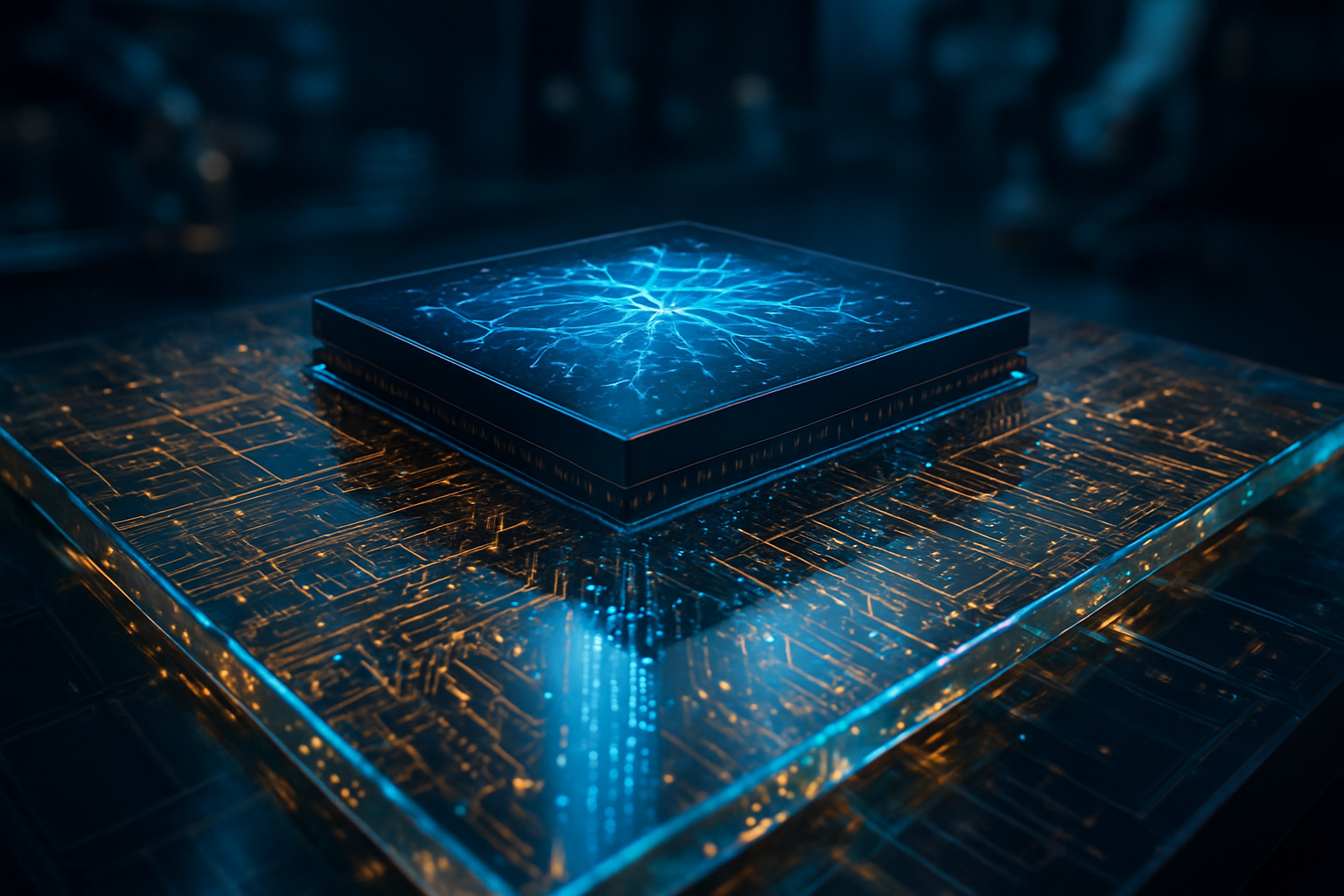
    On January 5, 2026, the landscape of autonomous sensing underwent a seismic shift as Tower Semiconductor (NASDAQ: TSEM) and LightIC Technologies announced a landmark strategic collaboration. The partnership is designed to mass-produce the next generation of Silicon Photonics (SiPho)-based 4D FMCW LiDAR, marking a pivotal moment where high-speed optical technology—once confined to the massive data centers powering Large Language Models—finally transitions into the "Physical AI" domain. This move promises to bring high-performance, velocity-aware sensing to autonomous vehicles and robotics at a scale and price point previously thought impossible.

    The collaboration leverages Tower Semiconductor’s mature 300mm SiPho foundry platform to manufacture LightIC’s proprietary Frequency-Modulated Continuous-Wave (FMCW) chips. By integrating complex optical engines—including lasers, modulators, and detectors—onto a single silicon substrate, the two companies are addressing the "SWaP-C" (Size, Weight, Power, and Cost) barriers that have long hindered the widespread adoption of high-end LiDAR. As AI models move from generating text to controlling physical "atoms" in robots and cars, this development provides the high-fidelity sensory input required for machines to navigate complex, dynamic human environments with unprecedented safety.

    The Technical Edge: 4D FMCW and the End of Optical Interference

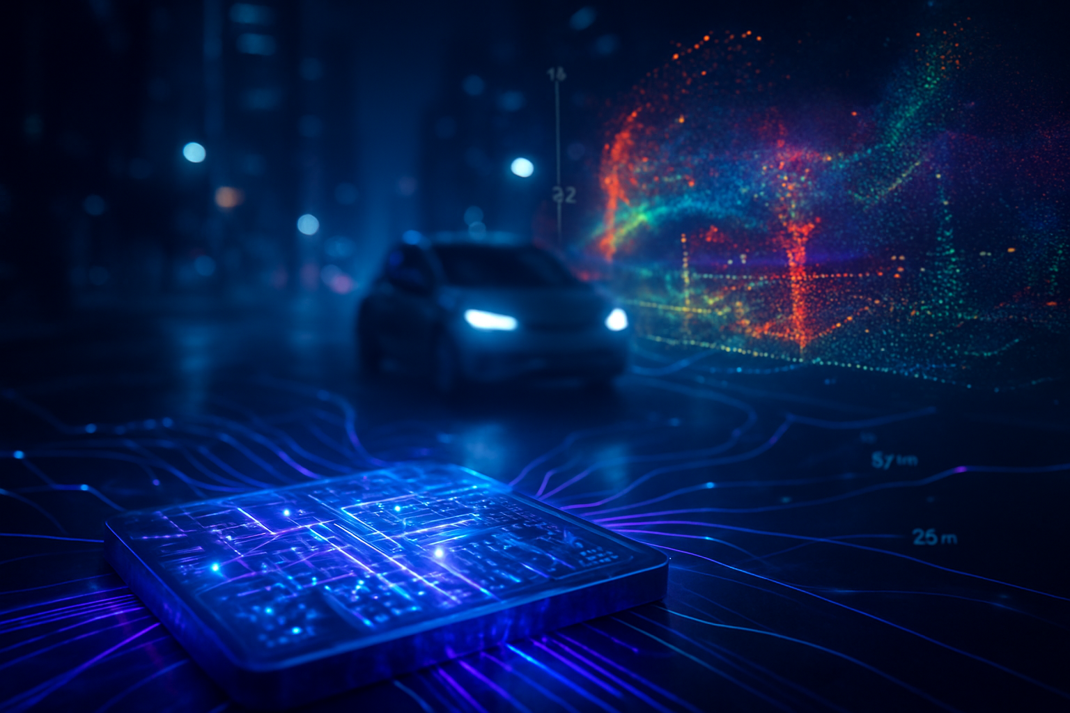
    At the heart of this announcement are two flagship products: the Lark™ for long-range automotive use and the FR60™ for compact robotics. Unlike traditional Time-of-Flight (ToF) LiDAR systems used by many current autonomous platforms, which measure distance by timing the reflection of light pulses, LightIC’s 4D FMCW technology measures both distance and instantaneous velocity simultaneously. The Lark™ system boasts a detection range of up to 300 meters and can identify objects at 500 meters, while providing velocity data with a precision of 0.05 m/s. This "4D" capability allows the AI to immediately distinguish between a stationary object and one moving toward the vehicle, drastically reducing the computational latency required for multi-frame tracking.

    Technically, the transition to SiPho allows these systems to operate at the 1550nm wavelength, which is inherently safer for human eyes and allows for higher power output than the 905nm lasers used in cheaper ToF systems. Furthermore, FMCW is naturally immune to optical interference. In a future where hundreds of autonomous vehicles might occupy the same highway, traditional LiDARs can "blind" each other with overlapping pulses. LightIC’s coherent detection ensures that each sensor only "hears" its own unique frequency-modulated signal, effectively eliminating the "crosstalk" problem that has plagued the industry.

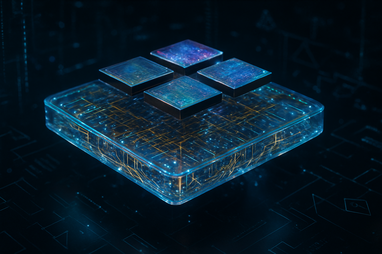
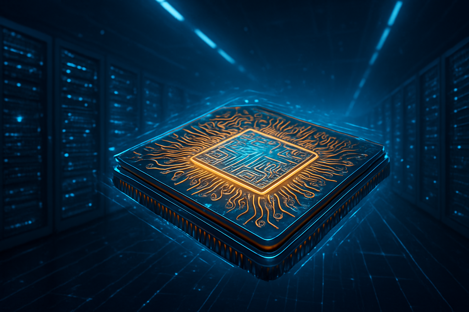
    The manufacturing process is equally significant. Tower Semiconductor utilizes its PH18 SiPho process and advanced wafer bonding to create a monolithic "LiDAR-on-a-chip." This differs from previous approaches that relied on discrete components—individual lasers and lenses—which are difficult to align and prone to failure under the vibrations of automotive use. By moving the entire optical bench onto a silicon chip, the partnership enables "image-grade" point clouds with an angular resolution of 0.1° x 0.08°, providing the resolution of a high-definition camera with the depth precision of a laser.

    Reshaping the Competitive Landscape: The Foundry Advantage

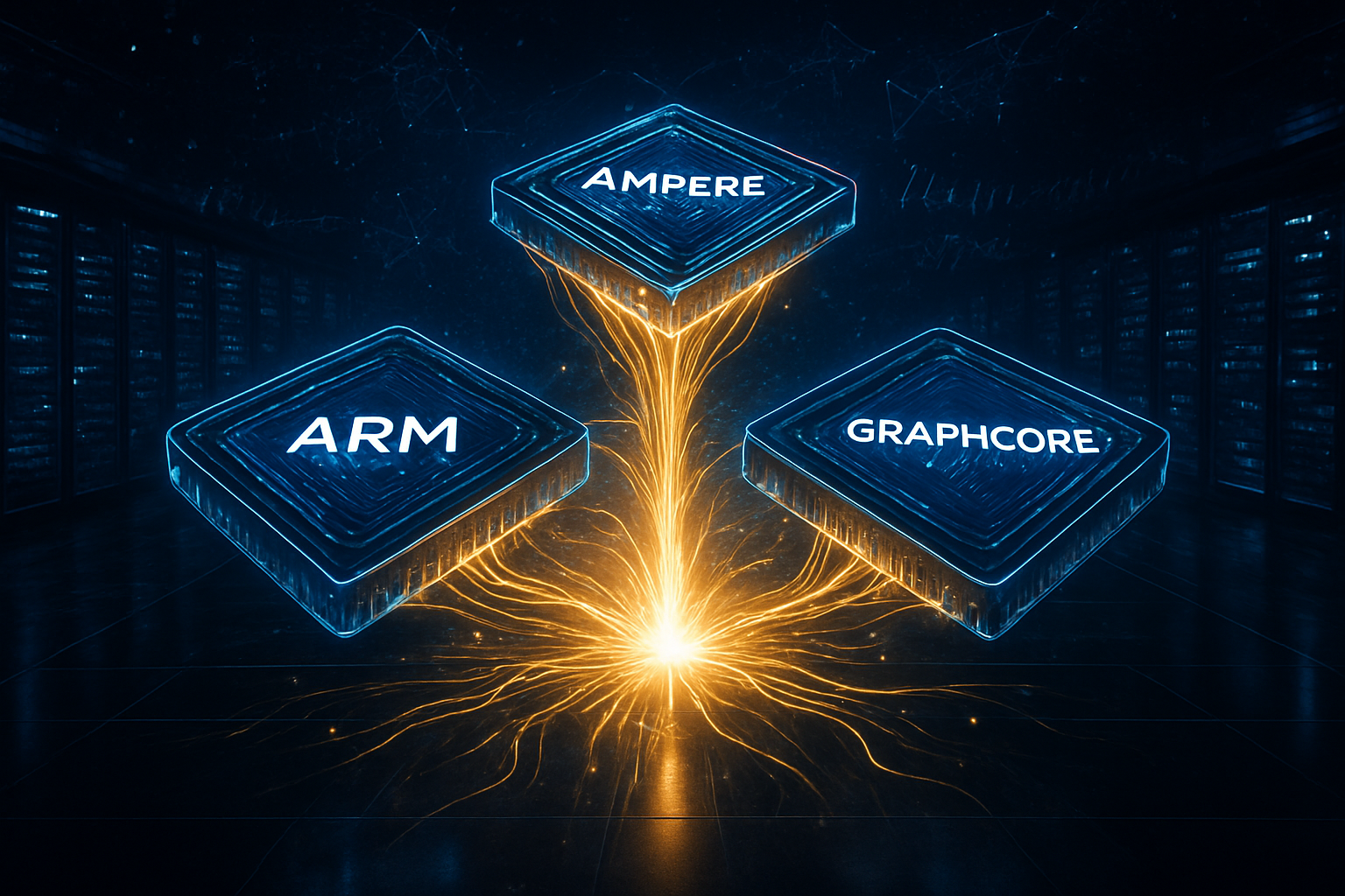
    This development is a direct challenge to established LiDAR players and represents a strategic win for the foundry model in photonics. While companies like Hesai Group (NASDAQ: HSAI) and Luminar Technologies (NASDAQ: LAZR) have made strides in automotive integration, the Tower-LightIC partnership brings the economies of scale associated with semiconductor giants. By utilizing the same 300mm manufacturing lines that produce 1.6Tbps optical transceivers for companies like NVIDIA Corporation (NASDAQ: NVDA), the partnership can drive down the cost of high-end LiDAR to levels that make it viable for mass-market consumer vehicles, not just luxury fleets or robotaxis.

    For AI labs and robotics startups, this announcement is a major enabler. The "Physical AI" movement—led by entities like Tesla, Figure, and Boston Dynamics—relies on high-quality training data. The ability to feed a neural network real-time, per-point velocity data rather than just 3D coordinates simplifies the "perception-to-action" pipeline. This could disrupt the current market for secondary sensors, potentially reducing the reliance on complex radar-camera fusion by providing a single, high-fidelity source of truth.

    Beyond Vision: The Arrival of "Velocity-Aware" Physical AI

    The broader significance of this expansion lies in the evolution of the AI landscape itself. For the past several years, the "AI Revolution" has been largely digital, focused on processing information within the cloud. In 2026, the trend has shifted toward "Embodied AI" or "Physical AI," where the challenge is to give silicon brains the ability to interact safely with the physical world. Silicon Photonics is the bridge for this transition. Just as CMOS image sensors revolutionized the smartphone era by making high-quality cameras ubiquitous, SiPho is poised to do the same for 3D sensing.

    The move from data centers to the edge is a natural progression. The photonics industry spent a decade perfecting the reliability and throughput of optical interconnects to handle the massive traffic of AI training clusters. That same reliability is now being applied to automotive safety. The implications for safety are profound: a vehicle equipped with 4D FMCW LiDAR can "see" the intention of a pedestrian or another vehicle through their instantaneous velocity, allowing for much faster emergency braking or evasive maneuvers. This level of "velocity awareness" is a milestone in the quest for Level 4 and Level 5 autonomy.

    The Road Ahead: Scaling Autonomy from Highways to Households

    In the near term, expect to see the Lark™ system integrated into high-end electric vehicle platforms scheduled for late 2026 and 2027 releases. The compact FR60™ is likely to find an immediate home in the logistics sector, powering the next generation of autonomous mobile robots (AMRs) in warehouses and "last-mile" delivery bots. The challenge moving forward will not be the hardware itself, but the software integration. AI developers will need to rewrite perception stacks to take full advantage of the 4D data stream, moving away from legacy algorithms designed for 3D ToF sensors.

    Experts predict that the success of the Tower-LightIC collaboration will spark a wave of consolidation in the LiDAR industry. Smaller players without access to high-volume SiPho foundries may struggle to compete on price and performance. As we look toward 2027, the goal will be "ubiquitous sensing"—integrating these chips into everything from household service robots to smart infrastructure. The "invisible AI" layer is becoming a reality, where the machines around us possess a sense of sight and motion that exceeds human capability.

    Conclusion: A New Foundation for Intelligent Machines

    The collaboration between Tower Semiconductor and LightIC Technologies marks the official entry of Silicon Photonics into the mainstream of Physical AI. By solving the dual challenges of interference and cost through advanced semiconductor manufacturing, they have provided the "eyes" that the next generation of AI requires. This is more than just a hardware upgrade; it is a foundational shift in how machines perceive reality.

    As we move through 2026, the industry will be watching for the first road tests of these integrated chips and the subsequent performance benchmarks from the robotics community. The transition of SiPho from the silent racks of data centers to the bustling streets of our cities is a testament to the technology's maturity. For the AI industry, the message is clear: the brain has been built, and now, it finally has the vision to match.


    This content is intended for informational purposes only and represents analysis of current AI developments.

    TokenRing AI delivers enterprise-grade solutions for multi-agent AI workflow orchestration, AI-powered development tools, and seamless remote collaboration platforms.
    For more information, visit https://www.tokenring.ai/.

  • The Glass Ceiling Shatters: How Glass Substrates are Redefining the Future of AI Accelerators

    The Glass Ceiling Shatters: How Glass Substrates are Redefining the Future of AI Accelerators

    As of early 2026, the semiconductor industry has reached a pivotal inflection point in the race to sustain the generative AI revolution. The traditional organic materials that have housed microchips for decades have officially hit a "warpage wall," threatening to stall the development of increasingly massive AI accelerators. In response, a high-stakes transition to glass substrates has moved from experimental laboratories to the forefront of commercial manufacturing, marking the most significant shift in chip packaging technology in over twenty years.

    This migration is not merely an incremental upgrade; it is a fundamental re-engineering of how silicon interacts with the physical world. By replacing organic resin with ultra-thin, high-strength glass, industry titans are enabling a 10x increase in interconnect density, allowing for the creation of "super-chips" that were previously impossible to manufacture. With Intel (NASDAQ: INTC), Samsung (KRX: 005930), and TSMC (NYSE: TSM) all racing to deploy glass-based solutions by 2026 and 2027, the battle for AI dominance has moved from the transistor level to the very foundation of the package.

    The Technical Breakthrough: Overcoming the Warpage Wall

    For years, the industry relied on Ajinomoto Build-up Film (ABF), an organic resin, to create the substrates that connect chips to circuit boards. however, as AI accelerators like those from NVIDIA (NASDAQ: NVDA) and AMD (NASDAQ: AMD) have grown larger and more power-hungry—often exceeding 1,000 watts of thermal design power—ABF has reached its physical limit. The primary culprit is the "warpage wall," a phenomenon caused by the mismatch in the Coefficient of Thermal Expansion (CTE) between silicon and organic materials. As these massive chips heat up and cool down, the organic substrate expands and contracts at a different rate than the silicon, causing the entire package to warp. This warping leads to cracked connections and "micro-bump" failures, effectively capping the size and complexity of next-generation AI hardware.

    Glass substrates solve this dilemma by offering a CTE that nearly matches silicon, providing unparalleled dimensional stability even at temperatures reaching 500°C. Beyond structural integrity, glass enables a massive leap in interconnect density through the use of Through-Glass Vias (TGVs). Unlike organic substrates, which require mechanical drilling that limits how closely connections can be spaced, glass can be etched with high-precision lasers. This allows for an interconnect pitch of less than 10 micrometers—a 10x improvement over the 100-micrometer pitch common in organic materials. This density is critical for the ultra-high-bandwidth memory (HBM4) and multi-die architectures required to train the next generation of Large Language Models (LLMs).

    Furthermore, glass provides superior electrical properties, reducing signal loss by up to 40% and cutting the power required for data movement by half. In an era where data center energy consumption is a global concern, the efficiency gains of glass are as valuable as its performance metrics. Initial reactions from the research community have been overwhelmingly positive, with experts noting that glass allows the industry to treat the entire package as a single, massive "system-on-wafer," effectively extending the life of Moore's Law through advanced packaging rather than just transistor scaling.

    The Corporate Race: Intel, Samsung, and the Triple Alliance

    The competition to bring glass substrates to market has ignited a fierce rivalry between the world’s leading foundries. Intel has taken an early lead, leveraging over a decade of research to establish a $1 billion commercial-grade pilot line in Chandler, Arizona. As of January 2026, Intel’s Chandler facility is actively producing glass cores for high-volume customers. This head start has allowed Intel Foundry to position glass packaging as a flagship differentiator, attracting cloud service providers who are designing custom AI silicon and need the thermal resilience that only glass can provide.

    Samsung has responded by forming a "Triple Alliance" that spans its most powerful divisions: Samsung Electronics, Samsung Display, and Samsung Electro-Mechanics. By repurposing the glass-processing expertise from its world-leading OLED and LCD businesses, Samsung has bypassed many of the supply chain hurdles that have slowed others. At the start of 2026, Samsung’s Sejong pilot line completed its final verification phase, with the company announcing at CES 2026 that it is on track for full-scale mass production by the end of the year. This integrated approach allows Samsung to offer an end-to-end glass solution, from the raw glass core to the final integrated AI package.

    Meanwhile, TSMC has pivoted toward a "rectangular revolution" known as Fan-Out Panel-Level Packaging (FO-PLP) on glass. By moving from traditional circular wafers to 600mm x 600mm rectangular glass panels, TSMC aims to increase area utilization from roughly 57% to over 80%, significantly lowering the cost of large-scale AI chips. TSMC’s branding for this effort, CoPoS (Chip-on-Panel-on-Substrate), is expected to be the successor to its industry-standard CoWoS technology. While TSMC is currently stabilizing yields on smaller 300mm panels at its Chiayi facility, the company is widely expected to ramp to full panel-level production by 2027, ensuring it remains the primary manufacturer for high-volume players like NVIDIA.

    Broader Significance: The Package is the New Transistor

    The shift to glass substrates represents a fundamental change in the AI landscape, signaling that the "package" has become as important as the "chip" itself. For the past decade, AI performance gains were largely driven by making transistors smaller. However, as we approach the physical limits of atomic-scale manufacturing, the bottleneck has shifted to how those transistors communicate and stay cool. Glass substrates remove this bottleneck, enabling the creation of 1-trillion-transistor packages that can span the size of an entire palm, a feat that would have been physically impossible with organic materials.

    This development also has profound implications for the geography of semiconductor manufacturing. Intel’s investment in Arizona and the emergence of Absolics (a subsidiary of SKC) in Georgia, USA, suggest that advanced packaging could become a cornerstone of the "onshoring" movement. By bringing high-end glass substrate production to the United States, these companies are shortening the supply chain for American AI giants like Microsoft (NASDAQ: MSFT) and Google (NASDAQ: GOOGL), who are increasingly reliant on custom-designed accelerators to run their massive AI workloads.

    However, the transition is not without its challenges. The fragility of glass during the manufacturing process remains a concern, requiring entirely new handling equipment and cleanroom protocols. Critics also point to the high initial cost of glass substrates, which may limit their use to the most expensive AI and high-performance computing (HPC) chips for the next several years. Despite these hurdles, the industry consensus is clear: without glass, the thermal and physical scaling of AI hardware would have hit a dead end.

    Future Horizons: Toward Optical Interconnects and 2027 Scaling

    Looking ahead, the roadmap for glass substrates extends far beyond simple structural support. By 2027, the industry expects to see the first wave of "Second Generation" glass packages that integrate silicon photonics directly into the substrate. Because glass is transparent, it allows for the seamless integration of optical interconnects, enabling chips to communicate using light rather than electricity. This would theoretically provide another order-of-magnitude jump in data transfer speeds while further reducing power consumption, a holy grail for the next decade of AI development.

    AMD is already in advanced evaluation phases for its MI400 series accelerators, which are rumored to be among the first to fully utilize these glass-integrated optical paths. As the technology matures, we can expect to see glass substrates trickle down from high-end data centers into high-performance consumer electronics, such as workstations for AI researchers and creators. The long-term vision is a modular "chiplet" ecosystem where different components from different manufacturers can be tiled onto a single glass substrate with near-zero latency between them.

    The primary challenge moving forward will be achieving the yields necessary for true mass-market adoption. While pilot lines are operational in early 2026, scaling to millions of units per month will require a robust global supply chain for high-purity glass and specialized laser-drilling equipment. Experts predict that 2026 will be the "year of the pilot," with 2027 serving as the true breakout year for glass-core AI hardware.

    A New Era for AI Infrastructure

    The industry-wide shift to glass substrates marks the end of the organic era for high-performance computing. By shattering the warpage wall and enabling a 10x leap in interconnect density, glass has provided the physical foundation necessary for the next decade of AI breakthroughs. Whether it is Intel's first-mover advantage in Arizona, Samsung's triple-division alliance, or TSMC's rectangular panel efficiency, the leaders of the semiconductor world have all placed their bets on glass.

    As we move through 2026, the success of these pilot lines will determine which companies lead the next phase of the AI gold rush. For investors and tech enthusiasts, the key metrics to watch will be the yield rates of these new facilities and the performance benchmarks of the first glass-backed AI accelerators hitting the market in the second half of the year. The transition to glass is more than a material change; it is the moment the semiconductor industry stopped building bigger chips and started building better systems.


    This content is intended for informational purposes only and represents analysis of current AI developments.

    TokenRing AI delivers enterprise-grade solutions for multi-agent AI workflow orchestration, AI-powered development tools, and seamless remote collaboration platforms.
    For more information, visit https://www.tokenring.ai/.

  • Japan’s Silicon Renaissance: Rapidus Hits 2nm GAA Milestone as Government Injects ¥1.23 Trillion into AI Future

    Japan’s Silicon Renaissance: Rapidus Hits 2nm GAA Milestone as Government Injects ¥1.23 Trillion into AI Future

    In a definitive stride toward reclaiming its status as a global semiconductor powerhouse, Japan’s state-backed venture Rapidus Corporation has successfully demonstrated the operational viability of its first 2nm Gate-All-Around (GAA) transistors. This technical breakthrough, achieved at the company’s IIM-1 facility in Hokkaido, marks a historic leap for a nation that had previously trailed the leading edge of logic manufacturing by nearly two decades. The success of these prototype wafers confirms that Japan has successfully bridged the gap from 40nm to 2nm, positioning itself as a legitimate contender in the race to power the next generation of artificial intelligence.

    The achievement is being met with unprecedented financial firepower from the Japanese government. As of early 2026, the Ministry of Economy, Trade and Industry (METI) has finalized a staggering ¥1.23 trillion ($7.9 billion) budget allocation for the 2026 fiscal year dedicated to semiconductors and domestic AI development. This massive capital infusion is designed to catalyze the transition from trial production to full-scale commercialization, ensuring that Rapidus meets its goal of launching an advanced packaging pilot line in April 2026, followed by mass production in 2027.

    Technical Breakthrough: The 2nm GAA Frontier

    The successful operation of 2nm GAA transistors represents a fundamental shift in semiconductor architecture. Unlike the traditional FinFET (Fin Field-Effect Transistor) design used in previous generations, the Gate-All-Around (nanosheet) structure allows the gate to contact the channel on all four sides. This provides superior electrostatic control, significantly reducing current leakage and power consumption while increasing drive current. Rapidus’s prototype wafers, processed using ASML (NASDAQ: ASML) Extreme Ultraviolet (EUV) lithography systems, have demonstrated electrical characteristics—including threshold voltage and leakage levels—that align with the high-performance requirements of modern AI accelerators.

    A key technical differentiator for Rapidus is its departure from traditional batch processing in favor of a "single-wafer processing" model. By processing wafers individually, Rapidus can utilize real-time AI-based monitoring and optimization at every stage of the manufacturing flow. This approach is intended to drastically reduce "turnaround time" (TAT), allowing customers to move from design to finished silicon much faster than the industry standard. This agility is particularly critical for AI startups and tech giants who are iterating on custom silicon designs at a blistering pace.

    The technical foundation for this achievement was laid through a deep partnership with IBM (NYSE: IBM) and the Belgium-based research hub imec. Since 2023, hundreds of Rapidus engineers have been embedded at the Albany NanoTech Complex in New York, working alongside IBM researchers to adapt the 2nm nanosheet technology IBM first unveiled in 2021. This collaboration has allowed Rapidus to leapfrog multiple generations of technology, effectively "importing" the world’s most advanced logic manufacturing expertise directly into the Japanese ecosystem.

    Shifting the Global Semiconductor Balance of Power

    The emergence of Rapidus as a viable 2nm manufacturer introduces a new dynamic into a market currently dominated by Taiwan Semiconductor Manufacturing Co. (NYSE: TSM) and Samsung Electronics (KRX: 005930). For years, the global supply chain has been heavily concentrated in Taiwan, creating significant geopolitical anxieties. Rapidus offers a high-tech alternative in a stable, democratic jurisdiction, which is already attracting interest from major AI players. Companies like Sony Group Corp (NYSE: SONY) and Toyota Motor Corp (TYO: 7203), both of which are investors in Rapidus, stand to benefit from a secure, domestic source of cutting-edge chips for autonomous driving and advanced image sensors.

    The strategic advantage for Rapidus lies in its focus on specialized, high-performance logic rather than high-volume commodity chips. By positioning itself as a "boutique" foundry for advanced AI silicon, Rapidus avoids a direct head-to-head war of attrition with TSMC’s massive scale. Instead, it offers a high-touch, fast-turnaround service for companies developing bespoke AI hardware. This model is expected to disrupt the existing foundry landscape, potentially pulling high-margin AI chip business away from traditional leaders as tech giants seek to diversify their supply chains.

    Furthermore, the Japanese government’s ¥1.23 trillion budget includes nearly ¥387 billion specifically for domestic AI foundational models. This creates a symbiotic relationship: Rapidus provides the hardware, while government-funded AI initiatives provide the demand. This "full-stack" national strategy ensures that the domestic ecosystem is not just a manufacturer for foreign firms, but a self-sustaining hub of AI innovation.

    Geopolitical Resilience and the "Last Chance" for Japan

    The "Rapidus Project" is frequently characterized by Japanese officials as the nation’s "last chance" to regain its 1980s-era dominance in the chip industry. During that decade, Japan controlled over half of the global semiconductor market, a share that has since dwindled to roughly 10%. The successful 2nm transistor operation is a psychological and economic turning point, proving that Japan can still compete at the bleeding edge. The massive 2026 budget allocation signals to the world that the Japanese state is no longer taking an "ad-hoc" approach to industrial policy, but is committed to long-term "technological sovereignty."

    This development also fits into a broader global trend of "onshoring" and "friend-shoring" critical technology. By establishing "Hokkaido Valley" in Chitose, Japan is creating a localized cluster of suppliers, engineers, and researchers. This regional hub is intended to insulate the Japanese economy from the volatility of US-China trade tensions. The inclusion of SoftBank Group Corp (TYO: 9984) and NEC Corp (TYO: 6701) among Rapidus’s backers underscores a unified national effort to ensure that the backbone of the digital economy—advanced logic—is produced on Japanese soil.

    However, the path forward is not without concerns. Critics point to the immense capital requirements—estimated at ¥5 trillion total—and the difficulty of maintaining high yields at the 2nm node. While the GAA transistor operation is a success, scaling that to millions of defect-free chips is a monumental task. Comparisons are often made to Intel Corp (NASDAQ: INTC), which has struggled with its own foundry transitions, highlighting the risks inherent in such an ambitious leapfrog strategy.

    The Road to April 2026 and Mass Production

    Looking ahead, the next critical milestone for Rapidus is April 2026, when the company plans to launch its advanced packaging pilot line at the "Rapidus Chiplet Solutions" (RCS) center. Advanced packaging, particularly chiplet technology, is becoming as important as the transistors themselves in AI applications. By integrating front-end 2nm manufacturing with back-end advanced packaging in the same geographic area, Rapidus aims to provide an end-to-end solution that further reduces production time and enhances performance.

    The near-term focus will be on "first light" exposures for early customer designs and optimizing the single-wafer processing flow. If the April 2026 packaging trial succeeds, Rapidus will be on track for its 2027 mass production target. Experts predict that the first wave of Rapidus-made chips will likely power high-performance computing (HPC) clusters and specialized AI edge devices for robotics, where Japan already holds a strong market position.

    The challenge remains the talent war. To succeed, Rapidus must continue to attract top-tier global talent to Hokkaido. The Japanese government is addressing this by funding university programs and research initiatives, but the competition for 2nm-capable engineers is fierce. The coming months will be a test of whether the "Hokkaido Valley" concept can generate the same gravitational pull as Silicon Valley or Hsinchu Science Park.

    A New Era for Japanese Innovation

    The successful operation of 2nm GAA transistors by Rapidus, backed by a monumental ¥1.23 trillion government commitment, marks the beginning of a new chapter in the history of technology. It is a bold statement that Japan is ready to lead once again in the most complex manufacturing process ever devised by humanity. By combining IBM’s architectural innovations with Japanese manufacturing precision and a unique single-wafer processing model, Rapidus is carving out a distinct niche in the AI era.

    The significance of this development cannot be overstated; it represents the most serious challenge to the existing semiconductor status quo in decades. As we move toward the April 2026 packaging trials, the world will be watching to see if Japan can turn this technical milestone into a commercial reality. For the global AI industry, the arrival of a third major player at the 2nm node promises more competition, more innovation, and a more resilient supply chain.

    The next few months will be critical as Rapidus begins installing the final pieces of its advanced packaging line and solidifies its first commercial contracts. For now, the successful "first light" of Japan’s 2nm ambition has brightened the prospects for a truly multipolar future in semiconductor manufacturing.


    This content is intended for informational purposes only and represents analysis of current AI developments.

    TokenRing AI delivers enterprise-grade solutions for multi-agent AI workflow orchestration, AI-powered development tools, and seamless remote collaboration platforms.
    For more information, visit https://www.tokenring.ai/.

  • Samsung’s SF2 Gamble: 2nm Exynos 2600 Challenges TSMC’s Dominance

    Samsung’s SF2 Gamble: 2nm Exynos 2600 Challenges TSMC’s Dominance

    As the calendar turns to early 2026, the global semiconductor landscape has reached a pivotal inflection point with the official arrival of the 2nm era. Samsung Electronics (KRX:005930) has formally announced the mass production of its SF2 (2nm) process, a technological milestone aimed squarely at reclaiming the manufacturing crown from its primary rival, Taiwan Semiconductor Manufacturing Company (NYSE:TSM). The centerpiece of this rollout is the Exynos 2600, a next-generation mobile processor codenamed "Ulysses," which is set to power the upcoming Galaxy S26 series.

    This development is more than a routine hardware refresh; it represents Samsung’s strategic "all-in" bet on Gate-All-Around (GAA) transistor architecture. By integrating the SF2 node into its flagship consumer devices, Samsung is attempting to prove that its third-generation Multi-Bridge Channel FET (MBCFET) technology can finally match or exceed the stability and performance of TSMC’s 2nm offerings. The immediate significance lies in the Exynos 2600’s ability to handle the massive compute demands of on-device generative AI, which has become the primary battleground for smartphone manufacturers in 2026.

    The Technical Edge: BSPDN and the 25% Efficiency Leap

    The transition to the SF2 node brings a suite of architectural advancements that represent a significant departure from the previous 3nm (SF3) generation. Most notably, Samsung has targeted a 25% improvement in power efficiency at equivalent clock speeds. This gain is achieved through the refinement of the MBCFET architecture, which allows for better electrostatic control and reduced leakage current. While initial production yields are estimated to be between 50% and 60%—a marked improvement over the company's early 3nm struggles—the SF2 node is already delivering a 12% performance boost and a 5% reduction in total chip area.

    A critical component of this efficiency story is the introduction of preliminary Backside Power Delivery Network (BSPDN) optimizations. While the full, "pure" implementation of BSPDN is slated for the SF2Z node in 2027, the Exynos 2600 utilizes a precursor routing technology that moves several power rails to the rear of the wafer. This reduces the "IR drop" (voltage drop) and mitigates the congestion between power and signal lines that has plagued traditional front-side delivery systems. Industry experts note that this "backside-first" approach is a calculated risk to outpace TSMC, which is not expected to introduce its own version of backside power delivery until the N2P node later this year.

    The Exynos 2600 itself is a technical powerhouse, featuring a 10-core CPU configuration based on the latest ARM v9.3 platform. It debuts the AMD Juno GPU (Xclipse 960), which Samsung claims provides a 50% improvement in ray-tracing performance over the Galaxy S25. More importantly, the chip's Neural Processing Unit (NPU) has seen a 113% throughput increase, specifically optimized for running large language models (LLMs) locally on the device. This allows the Galaxy S26 to perform complex AI tasks, such as real-time video translation and generative image editing, without relying on cloud-based servers.

    The Battle for Big Tech: Taylor, Texas as a Strategic Magnet

    Samsung’s 2nm ambitions extend far beyond its own Galaxy handsets. The company is aggressively positioning its $44 billion mega-fab in Taylor, Texas, as the premier "sovereign" foundry for North American tech giants. By pivoting the Taylor facility to 2nm production ahead of schedule, Samsung is courting "Big Tech" customers like NVIDIA (NASDAQ:NVDA), Apple (NASDAQ:AAPL), and Qualcomm (NASDAQ:QCOM) who are eager to diversify their supply chains away from a Taiwan-centric model.

    The strategy appears to be yielding results. Samsung has already secured a landmark $16.5 billion agreement with Tesla (NASDAQ:TSLA) to manufacture next-generation AI5 and AI6 chips for autonomous driving and the Optimus robotics program. Furthermore, AI silicon startups such as Groq and Tenstorrent have signed on as early 2nm customers, drawn by Samsung’s competitive pricing. Reports suggest that Samsung is offering 2nm wafers for approximately $20,000, significantly undercutting TSMC’s reported $30,000 price tag. This aggressive pricing, combined with the logistical advantages of a U.S.-based fab, has forced TSMC to accelerate its own Arizona-based production timelines.

    However, the competitive landscape remains fierce. While Samsung has the advantage of being the only firm with three generations of GAA experience, TSMC’s N2 node has already entered volume production with Apple as its lead customer. Apple has reportedly secured over 50% of TSMC’s initial 2nm capacity for its upcoming A20 and M6 chips. The market positioning is clear: TSMC remains the "premium" choice for established giants with massive budgets, while Samsung is positioning itself as the high-performance, cost-effective alternative for the next wave of AI hardware.

    Wider Significance: Sovereign AI and the End of Moore’s Law

    The 2nm race is a microcosm of the broader shift toward "Sovereign AI"—the desire for nations and corporations to control the physical infrastructure that powers their intelligence systems. Samsung’s success in Texas is a litmus test for the U.S. CHIPS Act and the feasibility of domestic high-end manufacturing. If Samsung can successfully scale the SF2 process in the United States, it will validate the multi-billion dollar subsidies provided by the federal government and provide a blueprint for other international firms like Intel (NASDAQ:INTC) to follow.

    This milestone also highlights the increasing difficulty of maintaining Moore’s Law. As transistors shrink to the 2nm level, the physics of electron tunneling and heat dissipation become exponentially harder to manage. The shift to GAA and BSPDN are not just incremental updates; they are fundamental re-architecturings of the transistor itself. This transition mirrors the industry's move from planar to FinFET transistors a decade ago, but with much higher stakes. Any yield issues at this level can result in billions of dollars in lost revenue, making Samsung's relatively stable 2nm pilot production a major psychological victory for the company's foundry division.

    The Road to 1.4nm and Beyond

    Looking ahead, the SF2 node is merely the first step in a long-term roadmap. Samsung has already begun detailing its SF2Z process for 2027, which will feature a fully optimized Backside Power Delivery Network to further boost density. Beyond that, the company is targeting 2028 for the mass production of its SF1.4 (1.4nm) node, which is expected to introduce "Vertical-GAA" structures to keep the scaling momentum alive.

    In the near term, the focus will shift to the real-world performance of the Galaxy S26. If the Exynos 2600 can finally close the efficiency gap with Qualcomm’s Snapdragon series, it will restore consumer faith in Samsung’s in-house silicon. Furthermore, the industry is watching for the first "made in Texas" 2nm chips to roll off the line in late 2026. Challenges remain, particularly in scaling the Taylor fab’s capacity to 100,000 wafers per month while maintaining the high yields required for profitability.

    Summary and Outlook

    Samsung’s SF2 announcement marks a bold attempt to leapfrog the competition by leveraging its early lead in GAA technology and its strategic investment in U.S. manufacturing. With a 25% efficiency target and the power of the Exynos 2600, the company is making a compelling case for its 2nm ecosystem. The inclusion of early-stage backside power delivery and the securing of high-profile clients like Tesla suggest that Samsung is no longer content to play second fiddle to TSMC.

    As we move through 2026, the success of this development will be measured by the market reception of the Galaxy S26 and the operational efficiency of the Taylor, Texas foundry. For the AI industry, this competition is a net positive, driving down costs and accelerating the hardware breakthroughs necessary for the next generation of intelligent machines. The coming weeks will be critical as early benchmarks for the Exynos 2600 begin to surface, providing the first definitive proof of whether Samsung has truly closed the gap.


    This content is intended for informational purposes only and represents analysis of current AI developments.

    TokenRing AI delivers enterprise-grade solutions for multi-agent AI workflow orchestration, AI-powered development tools, and seamless remote collaboration platforms.
    For more information, visit https://www.tokenring.ai/.

  • TSMC Officially Enters 2nm Mass Production: Apple and NVIDIA Lead the Charge into the GAA Era

    TSMC Officially Enters 2nm Mass Production: Apple and NVIDIA Lead the Charge into the GAA Era

    In a move that signals the dawn of a new era in computational power, Taiwan Semiconductor Manufacturing Company (NYSE: TSM) has officially entered volume mass production of its highly anticipated 2-nanometer (N2) process node. As of early January 2026, the company’s "Gigafabs" in Hsinchu and Kaohsiung have reached a steady output of over 50,000 wafers per month, marking the most significant architectural leap in semiconductor manufacturing in over a decade. This transition from the long-standing FinFET transistor design to the revolutionary Nanosheet Gate-All-Around (GAA) architecture promises to redefine the limits of energy efficiency and performance for the next generation of artificial intelligence and consumer electronics.

    The immediate significance of this milestone cannot be overstated. With the global AI race accelerating, the demand for more transistors packed into smaller, more efficient spaces has reached a fever pitch. By successfully ramping up the N2 node, TSMC has effectively cornered the high-end silicon market for the foreseeable future. Industry giants Apple (NASDAQ: AAPL) and NVIDIA (NASDAQ: NVDA) have already moved to lock up the entirety of the initial production capacity, ensuring that their 2026 flagship products—ranging from the iPhone 18 to the most advanced AI data center GPUs—will maintain a hardware advantage that competitors may find impossible to bridge in the near term.

    A Paradigm Shift in Transistor Design: The Nanosheet GAA Revolution

    The technical foundation of the N2 node is the shift to Nanosheet Gate-All-Around (GAA) transistors, a departure from the FinFET (Fin Field-Effect Transistor) structure that has dominated the industry since the 22nm era. In a GAA architecture, the gate surrounds the channel on all four sides, providing superior electrostatic control. This precision allows for significantly reduced current leakage and a massive leap in efficiency. According to TSMC’s technical disclosures, the N2 process offers a staggering 30% reduction in power consumption at the same speed compared to the previous N3E (3nm) node, or a 10-15% performance boost at the same power envelope.

    Beyond the transistor architecture, TSMC has integrated several key innovations to support the high-performance computing (HPC) demands of the AI era. This includes the introduction of Super High-Performance Metal-Insulator-Metal (SHPMIM) capacitors, which double the capacitance density. This technical addition is crucial for stabilizing power delivery to the massive, power-hungry logic arrays found in modern AI accelerators. While the initial N2 node does not yet feature backside power delivery—a feature reserved for the upcoming N2P variant—the density gains are still substantial, with logic-only designs seeing a nearly 20% increase in transistor density over the 3nm generation.

    Initial reactions from the semiconductor research community have been overwhelmingly positive, particularly regarding TSMC's reported yield rates. While rivals have struggled to maintain consistency with GAA technology, TSMC is estimated to have achieved yields in the 65-70% range for early production lots. This reliability is a testament to the company's "dual-hub" strategy, which utilizes Fab 20 in the Hsinchu Science Park and Fab 22 in Kaohsiung to scale production simultaneously. This approach has allowed TSMC to bypass the "yield valley" that often plagues the first year of a new process node, providing a stable supply chain for its most critical partners.

    The Power Play: How Tech Giants Are Securing the Future

    The move to 2nm has ignited a strategic scramble among the world’s largest technology firms. Apple has once again asserted its dominance as TSMC’s premier customer, reportedly reserving over 50% of the initial N2 capacity. This silicon is destined for the A20 Pro chips and the M6 series of processors, which are expected to power a new wave of "AI-first" devices. By securing this capacity, Apple ensures that its hardware remains the benchmark for mobile and laptop performance, potentially widening the gap between its ecosystem and competitors who may be forced to rely on older 3nm or 4nm technologies.

    NVIDIA has similarly moved with aggressive speed to secure 2nm wafers for its post-Blackwell architectures, specifically the "Rubin Ultra" and "Feynman" platforms. As the undisputed leader in AI training hardware, NVIDIA requires the 30% power efficiency gains of the N2 node to manage the escalating thermal and energy demands of massive data centers. By locking up capacity at Fab 20 and Fab 22, NVIDIA is positioning itself to deliver AI chips that can handle the next generation of trillion-parameter Large Language Models (LLMs) with significantly lower operational costs for cloud providers.

    This development creates a challenging landscape for other industry players. While AMD (NASDAQ: AMD) and Qualcomm (NASDAQ: QCOM) have also secured allocations, the "Apple and NVIDIA first" reality means that mid-tier chip designers and smaller AI startups may face higher prices and longer lead times. Furthermore, the competitive pressure on Intel (NASDAQ: INTC) and Samsung (KRX: 005930) has reached a critical point. While Intel’s 18A process technically reached internal production milestones recently, TSMC’s ability to deliver high-volume, high-yield 2nm silicon at scale remains its most potent competitive advantage, reinforcing its role as the indispensable foundry for the global economy.

    Geopolitics and the Global Silicon Map

    The commencement of 2nm production is not just a technical milestone; it is a geopolitical event. As TSMC ramps up its Taiwan-based facilities, it is also executing a parallel build-out of 2nm-capable capacity in the United States. Fab 21 in Arizona has seen its timelines accelerated under the influence of the U.S. CHIPS Act. While Phase 1 of the Arizona site is currently handling 4nm production, construction on Phase 3—the 2nm wing—is well underway. Current projections suggest that U.S.-based 2nm production could begin as early as 2028, providing a vital "geographic buffer" for the global supply chain.

    This expansion reflects a broader trend of "silicon sovereignty," where nations and companies are increasingly wary of the risks associated with concentrated manufacturing. However, the sheer complexity of the N2 node highlights why Taiwan remains the epicenter of the industry. The specialized workforce, local supply chain for chemicals and gases, and the proximity of R&D centers in Hsinchu create an "ecosystem gravity" that is difficult to replicate elsewhere. The 2nm node represents the pinnacle of human engineering, requiring Extreme Ultraviolet (EUV) lithography machines that are among the most complex tools ever built.

    Comparisons to previous milestones, such as the move to 7nm or 5nm, suggest that the 2nm transition will have a more profound impact on the AI landscape. Unlike previous nodes where the focus was primarily on mobile battery life, the 2nm node is being built from the ground up to support the massive throughput required for generative AI. The 30% power reduction is not just a luxury; it is a necessity for the sustainability of global data centers, which are currently consuming a growing share of the world's electricity.

    The Road to 1.4nm and Beyond

    Looking ahead, the N2 node is only the beginning of a multi-year roadmap that will see TSMC push even deeper into the angstrom era. By late 2026 and 2027, the company is expected to introduce N2P, an enhanced version of the 2nm process that will finally incorporate backside power delivery. This innovation will move the power distribution network to the back of the wafer, further reducing interference and allowing for even higher performance and density. Beyond that, the industry is already looking toward the A14 (1.4nm) node, which is currently in the early R&D phases at Fab 20’s specialized research wings.

    The challenges remaining are largely economic and physical. As transistors approach the size of a few dozen atoms, quantum tunneling and heat dissipation become existential threats to chip design. Moreover, the cost of designing a 2nm chip is estimated to be significantly higher than its 3nm predecessors, potentially pricing out all but the largest tech companies. Experts predict that this will lead to a "bifurcation" of the market, where a handful of elite companies use 2nm for flagship products, while the rest of the industry consolidates around mature, more affordable 3nm and 5nm nodes.

    Conclusion: A New Benchmark for the AI Age

    TSMC’s successful launch of the 2nm process node marks a definitive moment in the history of technology. By transitioning to Nanosheet GAA and achieving volume production in early 2026, the company has provided the foundation upon which the next decade of AI innovation will be built. The 30% power reduction and the massive capacity bookings by Apple and NVIDIA underscore the vital importance of this silicon in the modern power structure of the tech industry.

    As we move through 2026, the focus will shift from the "how" of manufacturing to the "what" of application. With the first 2nm-powered devices expected to hit the market by the end of the year, the world will soon see the tangible results of this engineering marvel. Whether it is more capable on-device AI assistants or more efficient global data centers, the ripples of TSMC’s N2 node will be felt across every sector of the economy. For now, the silicon crown remains firmly in Taiwan, as the world watches the Arizona expansion and the inevitable march toward the 1nm frontier.


    This content is intended for informational purposes only and represents analysis of current AI developments.

    TokenRing AI delivers enterprise-grade solutions for multi-agent AI workflow orchestration, AI-powered development tools, and seamless remote collaboration platforms.
    For more information, visit https://www.tokenring.ai/.

  • Intel Reclaims the Silicon Throne: 18A Node Enters Mass Production with Landmark Panther Lake Launch at CES 2026

    Intel Reclaims the Silicon Throne: 18A Node Enters Mass Production with Landmark Panther Lake Launch at CES 2026

    At CES 2026, Intel (NASDAQ: INTC) has officially signaled the end of its multi-year turnaround strategy by announcing the high-volume manufacturing (HVM) of its 18A process node and the immediate launch of the Core Ultra Series 3 processors, codenamed "Panther Lake." This announcement marks a pivotal moment in semiconductor history, as Intel becomes the first chipmaker to successfully deploy gate-all-around (GAA) transistors and backside power delivery at a massive commercial scale, effectively leapfrogging competitors in the race for transistor density and energy efficiency.

    The immediate significance of the Panther Lake launch cannot be overstated. By delivering a staggering 120 TOPS (Tera Operations Per Second) of AI performance from its integrated Arc B390 GPU alone, Intel is moving the "AI PC" from a niche marketing term into a powerhouse reality. With over 200 laptop designs from major partners already slated for 2026, Intel is flooding the market with hardware capable of running complex, multi-modal AI models locally, fundamentally altering the relationship between personal computing and the cloud.

    The Technical Vanguard: RibbonFET, PowerVia, and the 120 TOPS Barrier

    The engineering heart of Panther Lake lies in the Intel 18A node, which introduces two revolutionary technologies: RibbonFET and PowerVia. RibbonFET, Intel's implementation of a gate-all-around transistor architecture, replaces the aging FinFET design that has dominated the industry for over a decade. By wrapping the gate around the entire channel, Intel has achieved a 15% frequency boost and a 25% reduction in power consumption. This is complemented by PowerVia, a world-first backside power delivery system that moves power routing to the bottom of the wafer. This innovation eliminates the "wiring congestion" that has plagued chip design, allowing for a 30% improvement in overall chip density and significantly more stable voltage delivery.

    On the graphics and AI front, the integrated Arc B390 GPU, built on the new Xe3 "Battlemage" architecture, is the star of the show. It delivers 120 TOPS of AI compute, contributing to a total platform performance of 180 TOPS when combined with the NPU 5 and CPU. This represents a massive 60% multi-threaded performance boost over the previous "Lunar Lake" generation. Initial reactions from the industry have been overwhelmingly positive, with hardware analysts noting that the Arc B390’s ability to outperform many discrete entry-level GPUs while remaining integrated into the processor die is a "game-changer" for thin-and-light laptop form factors.

    Shifting the Competitive Landscape: Intel Foundry vs. The World

    The successful ramp-up of 18A at Fab 52 in Arizona is a direct challenge to the dominance of TSMC. For the first time in years, Intel can credibly claim a process leadership position, a feat that provides a strategic advantage to its burgeoning Intel Foundry business. This development is already paying dividends; the sheer volume of partner support at CES 2026 is unprecedented. Industry giants including Acer (TPE: 2353), ASUS (TPE: 2357), Dell (NYSE: DELL), and HP (NYSE: HPQ) showcased over 200 unique PC designs powered by Panther Lake, ranging from ultra-portable 1kg business machines to dual-screen creator workstations.

    For tech giants and AI startups, this hardware provides a standardized, high-performance target for edge AI software. As Intel regains its footing, competitors like AMD and Qualcomm find themselves in a fierce arms race to match the efficiency of the 18A node. The market positioning of Panther Lake—offering the raw compute of a desktop-class "H-series" chip with the 27-plus-hour battery life of an ultra-efficient mobile processor—threatens to disrupt the existing hierarchy of the premium laptop market, potentially forcing a recalibration of product roadmaps across the entire industry.

    A New Era for the AI PC and Sovereign Manufacturing

    Beyond the specifications, the 18A breakthrough represents a broader shift in the global technology landscape. Panther Lake is the most advanced semiconductor product ever manufactured at scale on United States soil, a fact that Intel CEO Pat Gelsinger highlighted as a win for "technological sovereignty." As geopolitical tensions continue to influence supply chain strategies, Intel’s ability to produce leading-edge silicon domestically provides a level of security and reliability that is increasingly attractive to both government and enterprise clients.

    This milestone also marks the definitive arrival of the "AI PC" era. By moving 120 TOPS of AI performance into the integrated GPU, Intel is enabling a future where generative AI, real-time language translation, and complex coding assistants run entirely on-device, preserving user privacy and reducing latency. This mirrors previous industry-defining shifts, such as the introduction of the Centrino platform which popularized Wi-Fi, suggesting that AI capability will soon be as fundamental to a PC as internet connectivity.

    The Road to 14A and Beyond

    Looking ahead, the success of 18A is merely a stepping stone in Intel’s "five nodes in four years" roadmap. The company is already looking toward the 14A node, which is expected to integrate High-NA EUV lithography to push transistor density even further. In the near term, the industry is watching for "Clearwater Forest," the server-side counterpart to Panther Lake, which will bring these 18A efficiencies to the data center. Experts predict that the next major challenge will be software optimization; with 180 platform TOPS available, the onus is now on developers to create applications that can truly utilize this massive local compute overhead.

    Potential applications on the horizon include autonomous "AI agents" that can manage complex workflows across multiple professional applications without ever sending data to a central server. While challenges remain—particularly in managing the heat generated by such high-performance integrated graphics in ultra-thin chassis—Intel’s engineering team has expressed confidence that the architectural efficiency of RibbonFET provides enough thermal headroom for the next several years of innovation.

    Conclusion: Intel’s Resurgence Confirmed

    The launch of Panther Lake at CES 2026 is more than just a product release; it is a declaration that Intel has returned to the forefront of semiconductor innovation. By successfully transitioning the 18A node to high-volume manufacturing and delivering a 60% performance leap over its predecessor, Intel has silenced many of its skeptics. The combination of RibbonFET, PowerVia, and the 120-TOPS Arc B390 GPU sets a new benchmark for what consumers can expect from a modern personal computer.

    As the first wave of 200+ partner designs from Acer, ASUS, Dell, and HP hits the shelves in the coming months, the industry will be watching closely to see how this new level of local AI performance reshapes the software ecosystem. For now, the takeaway is clear: the race for AI supremacy has moved from the cloud to the silicon in your lap, and Intel has just taken a commanding lead.


    This content is intended for informational purposes only and represents analysis of current AI developments.

    TokenRing AI delivers enterprise-grade solutions for multi-agent AI workflow orchestration, AI-powered development tools, and seamless remote collaboration platforms.
    For more information, visit https://www.tokenring.ai/.

  • Breaking the Warpage Wall: The Semiconductor Industry Pivots to Glass Substrates for the Next Era of AI

    Breaking the Warpage Wall: The Semiconductor Industry Pivots to Glass Substrates for the Next Era of AI

    As of January 7, 2026, the global semiconductor industry has reached a critical inflection point. For decades, organic materials like Ajinomoto Build-up Film (ABF) served as the foundation for chip packaging, but the insatiable power and size requirements of modern Artificial Intelligence (AI) have finally pushed these materials to their physical limits. In a move that analysts are calling a "once-in-a-generation" shift, industry titans are transitioning to glass substrates—a breakthrough that promises to unlock a new level of performance for the massive, multi-die packages required for next-generation AI accelerators.

    The immediate significance of this development cannot be overstated. With AI chips now exceeding 1,000 watts of thermal design power (TDP) and reaching physical dimensions that would cause traditional organic substrates to warp or crack, glass provides the structural integrity and electrical precision necessary to keep Moore’s Law alive. This transition is not merely an incremental upgrade; it is a fundamental re-engineering of how the world's most powerful chips are built, enabling a 10x increase in interconnect density and a 40% reduction in signal loss.

    The Technical Leap: From Organic Polymers to Precision Glass

    The shift to glass substrates is driven by the failure of organic materials to scale alongside the "chiplet" revolution. Traditional organic substrates are prone to "warpage"—the physical deforming of the material under high temperatures—which limits the size of a chip package to roughly 55mm x 55mm. As AI GPUs from companies like NVIDIA (NASDAQ: NVDA) and AMD (NASDAQ: AMD) grow to 100mm x 100mm and beyond, the industry has hit what experts call the "warpage wall." Glass, with its superior thermal stability, remains flat even at temperatures exceeding 500°C, matching the coefficient of thermal expansion of silicon and preventing the catastrophic mechanical failures seen in organic designs.

    Technically, the most significant advancement lies in Through-Glass Vias (TGVs). Unlike the mechanical drilling used for organic substrates, TGVs are etched using high-precision lasers, allowing for an interconnect pitch of less than 10 micrometers—a 10x improvement over the 100-micrometer pitch common in organic materials. This density allows for significantly more "tiles" or chiplets to be packed into a single package, facilitating the massive memory bandwidth required for Large Language Models (LLMs). Furthermore, glass's ultra-low dielectric loss improves signal integrity by nearly 40%, which translates to a power consumption reduction of up to 50% for data movement within the chip.

    Initial reactions from the AI research community and industry experts have been overwhelmingly positive. At the recent CES 2026 "First Look" event, analysts noted that glass substrates are the "critical enabler" for 2.5D and 3D packaging. While organic substrates still dominate mainstream consumer electronics, the high-performance computing (HPC) sector has reached a consensus: without glass, the physical size of AI clusters would be capped by the mechanical limits of plastic, effectively stalling AI hardware progress.

    Competitive Landscapes: Intel, Samsung, and the Race for Packaging Dominance

    The transition to glass has sparked a fierce competition among the world’s leading foundries and IDMs. Intel Corporation (NASDAQ: INTC) has emerged as an early technical pioneer, having officially reached High-Volume Manufacturing (HVM) for its 18A node as of early 2026. Intel’s dedicated glass substrate facility in Chandler, Arizona, has successfully transitioned from pilot phases to supporting commercial-grade packaging. By offering glass-based solutions to its foundry customers, Intel is positioning itself as a formidable alternative to TSMC (NYSE: TSM), specifically targeting NVIDIA and AMD's high-end business.

    Samsung (KRX: 005930) is not far behind. Samsung Electro-Mechanics (SEMCO) has fast-tracked its "dream substrate" program, completing verification of its high-volume pilot line in Sejong, South Korea, in late 2025. Samsung announced at CES 2026 that it is on track for full-scale mass production by the end of the year. To bolster its competitive edge, Samsung has formed a "triple alliance" between its substrate, electronics, and display divisions, leveraging its expertise in glass processing from the smartphone and TV industries.

    Meanwhile, TSMC has been forced to pivot. Originally focused on silicon interposers (CoWoS), the Taiwanese giant revived its glass substrate R&D in late 2024 under intense pressure from its primary customer, NVIDIA. As of January 2026, TSMC is aggressively pursuing Fan-Out Panel-Level Packaging (FO-PLP) on glass. This "Rectangular Revolution" involves moving from 300mm circular silicon wafers to large 600mm x 600mm rectangular glass panels. This shift increases area utilization from 57% to over 80%, drastically reducing the "AI chip bottleneck" by allowing more chips to be packaged simultaneously and at a lower cost per unit.

    Wider Significance: Moore’s Law and the Energy Efficiency Frontier

    The adoption of glass substrates fits into a broader trend known as "More than Moore," where performance gains are achieved through advanced packaging rather than just transistor shrinking. As it becomes increasingly difficult and expensive to shrink transistors below the 2nm threshold, the ability to package multiple specialized chiplets together with high-speed, low-power interconnects becomes the primary driver of computing power. Glass is the medium that makes this "Lego-style" chip building possible at the scale required for future AI.

    Beyond raw performance, the move to glass has profound implications for energy efficiency. Data centers currently consume a significant portion of global electricity, with a large percentage of that energy spent moving data between processors and memory. By reducing signal attenuation and cutting power consumption by up to 50%, glass substrates offer a rare opportunity to improve the sustainability of AI infrastructure. This is particularly relevant as global regulators begin to scrutinize the carbon footprint of massive AI training clusters.

    However, the transition is not without concerns. Glass is inherently brittle, and manufacturers are currently grappling with breakage rates that are 5-10% higher than organic alternatives. This has necessitated entirely new automated handling systems and equipment from vendors like Applied Materials (NASDAQ: AMAT) and Coherent (NYSE: COHR). Furthermore, initial mass production yields are hovering between 70% and 75%, trailing the 90%+ maturity of organic substrates, leading to a temporary cost premium for the first generation of glass-packaged chips.

    Future Horizons: Optical I/O and the 2030 Roadmap

    Looking ahead, the near-term focus will be on stabilizing yields and standardizing panel sizes to bring down costs. Experts predict that while glass substrates currently carry a 3x to 5x cost premium, aggressive cost reduction roadmaps will see prices decline by 40-60% by 2030 as manufacturing scales. The first commercial products to feature full glass core integration are expected to hit the market in late 2026 and early 2027, likely appearing in NVIDIA’s "Rubin" architecture and AMD’s MI400 series accelerators.

    The long-term potential of glass extends into the realm of Silicon Photonics. Because glass is transparent and thermally stable, it is being positioned as the primary medium for Co-Packaged Optics (CPO). In this future scenario, data will be moved via light rather than electricity, virtually eliminating latency and power loss in AI clusters. Companies like Amazon (NASDAQ: AMZN) and SKC (KRX: 011790)—through its subsidiary Absolics—are already exploring how glass can facilitate this transition to optical computing.

    The primary challenge remains the "fragility gap." As chips become larger and more complex, the risk of a microscopic crack ruining a multi-thousand-dollar processor is a major hurdle. Experts predict that the next two years will see a surge in innovation regarding "tempered" glass substrates and specialized protective coatings to mitigate these risks.

    A Paradigm Shift in Semiconductor History

    The transition to glass substrates represents one of the most significant material changes in semiconductor history. It marks the end of the organic era for high-performance computing and the beginning of a new age where the package is as critical as the silicon it holds. By breaking the "warpage wall," Intel, Samsung, and TSMC are ensuring that the hardware requirements of artificial intelligence do not outpace the physical capabilities of our materials.

    Key takeaways from this shift include the 10x increase in interconnect density, the move toward rectangular panel-level packaging, and the critical role of glass in enabling future optical interconnects. While the transition is currently expensive and technically challenging, the performance benefits are too great to ignore. In the coming weeks and months, the industry will be watching for the first yield reports from Absolics’ Georgia facility and further details on NVIDIA’s integration of glass into its 2027 roadmap. The "Glass Age" of semiconductors has officially arrived.


    This content is intended for informational purposes only and represents analysis of current AI developments.

    TokenRing AI delivers enterprise-grade solutions for multi-agent AI workflow orchestration, AI-powered development tools, and seamless remote collaboration platforms.
    For more information, visit https://www.tokenring.ai/.

  • The Dawn of the AI PC Era: How Local NPUs are Transforming the Silicon Landscape

    The Dawn of the AI PC Era: How Local NPUs are Transforming the Silicon Landscape

    The dream of a truly personal computer—one that understands, anticipates, and assists without tethering itself to a distant data center—has finally arrived. As of January 2026, the "AI PC" is no longer a futuristic marketing buzzword or a premium niche; it has become the standard for modern computing. This week at CES 2026, the industry witnessed a definitive shift as the latest silicon from the world’s leading chipmakers officially moved the heavy lifting of artificial intelligence from the cloud directly onto the local silicon of our laptops and desktops.

    This transformation marks the most significant architectural shift in personal computing since the introduction of the graphical user interface. By integrating dedicated Neural Processing Units (NPUs) directly into the heart of the processor, companies like Intel and AMD have enabled a new class of "always-on" AI experiences. From real-time, multi-language translation during live calls to the local generation of high-resolution video, the AI PC era is fundamentally changing how we interact with technology, prioritizing privacy, reducing latency, and slashing the massive energy costs associated with cloud-based AI.

    The Silicon Arms Race: Panther Lake vs. Gorgon Point

    The technical foundation of this era rests on the unprecedented performance of new NPUs. Intel (NASDAQ: INTC) recently unveiled its Core Ultra Series 3, codenamed "Panther Lake," built on the cutting-edge Intel 18A manufacturing process. These chips feature the "NPU 5" architecture, which delivers a consistent 50 Trillions of Operations Per Second (TOPS) dedicated solely to AI tasks. When combined with the new Xe3 "Celestial" GPU and the high-efficiency CPU cores, the total platform performance can reach a staggering 180 TOPS. This allows Panther Lake to handle complex "Physical AI" tasks—such as real-time gesture tracking and environment mapping—without breaking a thermal sweat.

    Not to be outdone, AMD (NASDAQ: AMD) has launched its Ryzen AI 400 series, featuring the "Gorgon Point" architecture. AMD’s strategy has focused on "AI ubiquity," bringing high-performance NPUs to even mid-range and budget-friendly laptops. The Gorgon Point chips utilize an upgraded XDNA 2 NPU capable of 60 TOPS, slightly edging out Intel in raw NPU throughput for small language models (SLMs). This hardware allows Windows 11 to run advanced features like "Cocreator" and "Restyle Image" near-instantly, using local weights rather than sending data to a remote server.

    This shift differs from previous approaches by moving away from "General Purpose" computing. In the past, AI tasks were offloaded to the GPU, which, while powerful, is a massive power drain. The NPU is a specialized "XPU" designed specifically for the matrix mathematics required by neural networks. Initial reactions from the research community have been overwhelmingly positive, with experts noting that the 2026 generation of chips finally provides the "thermal headroom" necessary for AI to run in the background 24/7 without killing battery life.

    A Seismic Shift in the Tech Power Structure

    The rise of the AI PC is creating a new hierarchy among tech giants. Microsoft (NASDAQ: MSFT) stands as perhaps the biggest beneficiary, having successfully transitioned its entire Windows ecosystem to the "Copilot+ PC" standard. By mandating a minimum of 40 NPU TOPS for its latest OS features, Microsoft has effectively forced a hardware refresh cycle. This was perfectly timed with the end of support for Windows 10 in late 2025, leading to a massive surge in enterprise upgrades. Businesses are now pivoting toward AI PCs to reduce "inference debt"—the recurring costs of paying for cloud-based AI APIs from providers like OpenAI or Google (NASDAQ: GOOGL).

    The competitive implications are equally stark for the mobile-first chipmakers. While Qualcomm (NASDAQ: QCOM) sparked the AI PC trend in 2024 with the Snapdragon X Elite, the 2026 resurgence of x86 dominance from Intel and AMD shows that traditional chipmakers have successfully closed the efficiency gap. By leveraging advanced nodes like Intel 18A, x86 chips now offer the same "all-day" battery life as ARM-based alternatives while maintaining superior compatibility with legacy enterprise software. This has put pressure on Apple (NASDAQ: AAPL), which, despite pioneering integrated NPUs with its M-series, now faces a Windows ecosystem that is more open and increasingly competitive in AI performance-per-watt.

    Furthermore, software giants like Adobe (NASDAQ: ADBE) are being forced to re-architect their creative suites. Instead of relying on "Cloud Credits" for generative fill or video upscaling, the 2026 versions of Photoshop and Premiere Pro are optimized to detect the local NPU. This disrupts the current SaaS (Software as a Service) model, shifting the value proposition from cloud-based "magic" to local, hardware-accelerated productivity.

    Privacy, Latency, and the Death of the Cloud Tether

    The wider significance of the AI PC era lies in the democratization of privacy. In 2024, Microsoft faced significant backlash over "Windows Recall," a feature that took snapshots of user activity. In 2026, the narrative has flipped. Thanks to the power of local NPUs, Recall data is now encrypted and stored in a "Secure Zone" on the chip, never leaving the device. This "Local-First" AI model is a direct response to growing consumer anxiety over data harvesting. When your PC translates a private business call or generates a sensitive document locally, the risk of a data breach is virtually eliminated.

    Beyond privacy, the impact on global bandwidth is profound. As AI PCs handle more generative tasks locally, the strain on global data centers is expected to plateau. This fits into the broader "Edge AI" trend, where intelligence is pushed to the periphery of the network. We are seeing a move away from the "Thin Client" philosophy of the last decade and a return to the "Fat Client," where the local machine is the primary engine of creation.

    However, this transition is not without concerns. There is a growing "AI Divide" between those who can afford the latest NPU-equipped hardware and those stuck on "legacy" systems. As software developers increasingly optimize for NPUs, older machines may feel significantly slower, not because their CPUs are weak, but because they lack the specialized silicon required for the modern, AI-integrated operating system.

    The Road Ahead: Agentic AI and Physical Interaction

    Looking toward the near future, the next frontier for the AI PC is "Agentic AI." While today’s systems are reactive—responding to prompts—the late 2026 and 2027 roadmaps suggest a shift toward proactive agents. These will be local models that observe your workflow across different apps and perform complex, multi-step tasks autonomously, such as "organizing all receipts from last month into a spreadsheet and flagging discrepancies."

    We are also seeing the emergence of "Physical AI" applications. With the high TOPS counts of 2026 hardware, PCs are becoming capable of processing high-fidelity spatial data. This will enable more immersive augmented reality (AR) integrations and sophisticated eye-tracking and gesture-based interfaces that feel natural rather than gimmicky. The challenge remains in standardization; while Microsoft has set the baseline with Copilot+, a unified API that allows developers to write one AI application that runs seamlessly across Intel, AMD, and Qualcomm silicon is still a work in progress.

    A Landmark Moment in Computing History

    The dawn of the AI PC era represents the final transition of the computer from a tool we use to a collaborator we work with. The developments seen in early 2026 confirm that the NPU is now as essential to the motherboard as the CPU itself. The key takeaways are clear: local AI is faster, more private, and increasingly necessary for modern software.

    As we look ahead, the significance of this milestone will likely be compared to the transition from command-line interfaces to Windows. The AI PC has effectively "humanized" the machine. In the coming months, watch for the first wave of "NPU-native" applications that move beyond simple chatbots and into true, local workflow automation. The "Crossover Year" has passed, and the era of the intelligent, autonomous personal computer is officially here.


    This content is intended for informational purposes only and represents analysis of current AI developments.

    TokenRing AI delivers enterprise-grade solutions for multi-agent AI workflow orchestration, AI-powered development tools, and seamless remote collaboration platforms.
    For more information, visit https://www.tokenring.ai/.

  • SoftBank’s $6.5 Billion Ampere Acquisition: The Dawn of the AI Silicon Trinity

    SoftBank’s $6.5 Billion Ampere Acquisition: The Dawn of the AI Silicon Trinity

    The global landscape of artificial intelligence infrastructure shifted decisively this week as SoftBank Group Corp. (OTC: SFTBY) finalized its $6.5 billion acquisition of Ampere Computing. The deal, which officially closed on November 25, 2025, represents the latest and perhaps most critical piece in Masayoshi Son’s ambitious "Artificial Super Intelligence" (ASI) roadmap. By bringing the world’s leading independent ARM-based server chip designer under its roof, SoftBank has effectively transitioned from a venture capital powerhouse into a vertically integrated industrial giant capable of controlling the hardware that will power the next decade of AI evolution.

    The acquisition marks a strategic pivot for SoftBank, which has spent the last year consolidating its grip on the semiconductor supply chain. With the addition of Ampere, SoftBank now owns a formidable "Silicon Trinity" consisting of Arm Holdings plc (Nasdaq: ARM) for architecture, the recently acquired Graphcore for AI acceleration, and Ampere for server-side processing. This integration is designed to solve the massive power and efficiency bottlenecks currently plaguing hyperscale data centers as they struggle to meet the insatiable compute demands of generative AI and emerging autonomous systems.

    The Technical Edge: 512 Cores and the Death of x86 Dominance

    At the heart of this acquisition is Ampere’s revolutionary "cloud-native" processor architecture. Unlike traditional incumbents like Intel Corporation (Nasdaq: INTC) and Advanced Micro Devices, Inc. (Nasdaq: AMD), which have spent decades refining the x86 architecture for general-purpose computing, Ampere built its chips from the ground up using the ARM instruction set. The technical crowning jewel of the deal is the "AmpereOne Aurora," a massive 512-core processor slated for widespread deployment in 2026. This chip utilizes custom-designed cores that prioritize predictable performance and high-density throughput, allowing data centers to pack more processing power into a smaller physical footprint.

    The technical distinction lies in Ampere’s ability to handle "AI inference" workloads—the process of running trained AI models—with significantly higher efficiency than traditional CPUs. While NVIDIA Corporation (Nasdaq: NVDA) GPUs remain the gold standard for training large language models, those GPUs require powerful, energy-efficient CPUs to act as "host" processors to manage data flow. Ampere’s ARM-based designs eliminate the "IO bottleneck" often found in x86 systems, ensuring that expensive AI accelerators aren't left idling while waiting for data.

    Industry experts have noted that the AmpereOne Aurora’s performance-per-watt is nearly double that of current-generation x86 server chips. In an era where power availability has become the primary constraint for AI expansion, this efficiency is not just a cost-saving measure but a fundamental requirement for scaling. The AI research community has largely reacted with optimism, noting that a standardized ARM-based server platform could simplify software development for AI researchers who are increasingly moving away from hardware-specific optimizations.

    A Strategic Masterstroke in the AI Arms Race

    The market implications of this deal are profound, particularly for the major cloud service providers. Oracle Corporation (NYSE: ORCL), an early backer of Ampere, has already integrated these chips deeply into its cloud infrastructure, and the acquisition ensures a stable, SoftBank-backed roadmap for other giants like Microsoft Corporation (Nasdaq: MSFT) and Alphabet Inc. (Nasdaq: GOOGL). By controlling Ampere, SoftBank can now offer a unified hardware-software stack that bridges the gap between the mobile-centric ARM ecosystem and the high-performance computing required for AI.

    For competitors like Intel and AMD, the SoftBank-Ampere alliance represents a direct existential threat in the data center market. For years, x86 was the undisputed king of the server room, but the AI boom has exposed its limitations in power efficiency and multi-core scalability. SoftBank’s ownership of Arm Holdings allows for "deep taping out" synergies, where the architectural roadmap of ARM can be co-developed with Ampere’s physical chip implementations. This creates a feedback loop that could allow SoftBank to bring AI-optimized silicon to market months or even years faster than traditional competitors.

    Furthermore, the acquisition positions SoftBank as a key player in "Project Stargate," the rumored $500 billion infrastructure initiative aimed at building the world's largest AI supercomputers. With Ampere chips serving as the primary compute host, SoftBank is no longer just a supplier of intellectual property; it is the architect of the physical infrastructure upon which the future of AI will be built. This strategic positioning gives Masayoshi Son immense leverage over the direction of the entire AI industry.

    Energy, Sovereignty, and the Broader AI Landscape

    Beyond the balance sheets, the SoftBank-Ampere deal addresses the growing global concern over energy consumption in the AI era. As AI models grow in complexity, the carbon footprint of the data centers that house them has come under intense scrutiny. Ampere’s "Sustainable Compute" philosophy aligns with a broader industry trend toward "Green AI." By reducing the power required for inference, SoftBank is positioning itself as the "responsible" choice for governments and corporations under pressure to meet ESG (Environmental, Social, and Governance) targets.

    This acquisition also touches on the sensitive issue of "technological sovereignty." As nations race to build their own domestic AI capabilities, the ability to access high-performance, non-x86 hardware becomes a matter of national security. SoftBank’s global footprint and its base in Japan provide a neutral alternative to the US-centric dominance of Intel and NVIDIA, potentially opening doors for massive infrastructure projects in Europe, the Middle East, and Asia.

    However, the consolidation of such critical technology under one roof has raised eyebrows among antitrust advocates. With SoftBank owning the architecture (ARM), the server chips (Ampere), and the accelerators (Graphcore), there are concerns about a "walled garden" effect. Critics argue that this level of vertical integration could stifle innovation from smaller chip startups that rely on ARM licenses but now find themselves competing directly with their licensor’s parent company.

    The Horizon: From Inference to Autonomy

    Looking ahead, the integration of Ampere into the SoftBank ecosystem is expected to accelerate the development of "Edge AI"—bringing powerful AI capabilities out of the data center and into robots, autonomous vehicles, and industrial IoT devices. The near-term focus will be on the 2026 rollout of the 512-core Aurora chips, but the long-term vision involves a seamless compute fabric where a single architecture scales from a smartwatch to a massive AI supercluster.

    The biggest challenge facing SoftBank will be the execution of this integration. Merging the corporate cultures of a British IP firm (ARM), a British AI startup (Graphcore), and a Silicon Valley chip designer (Ampere) under a Japanese conglomerate is a monumental task. Furthermore, the industry is watching closely to see how SoftBank manages its relationship with other ARM licensees who may now view the company as a direct competitor rather than a neutral partner.

    A New Era for AI Hardware

    The acquisition of Ampere Computing for $6.5 billion is more than just a line item in SoftBank’s portfolio; it is a declaration of intent. It marks the end of the "software-first" era of AI and the beginning of the "infrastructure-first" era. By securing the most efficient server technology on the market, SoftBank has insured itself against the volatility of the AI software market and anchored its future in the physical reality of silicon and power.

    As we move into 2026, the industry will be watching for the first "Trinity" systems—servers that combine ARM architecture, Ampere CPUs, and Graphcore accelerators into a single, optimized unit. If Masayoshi Son’s gamble pays off, the "Silicon Trinity" could become the standard blueprint for the AI age, fundamentally altering the power dynamics of the technology world for decades to come.


    This content is intended for informational purposes only and represents analysis of current AI developments.

    TokenRing AI delivers enterprise-grade solutions for multi-agent AI workflow orchestration, AI-powered development tools, and seamless remote collaboration platforms.
    For more information, visit https://www.tokenring.ai/.

  • The Great Silicon Pivot: How Huawei’s Ascend Ecosystem is Rewiring China’s AI Ambitions

    The Great Silicon Pivot: How Huawei’s Ascend Ecosystem is Rewiring China’s AI Ambitions

    As of early 2026, the global artificial intelligence landscape has fractured into two distinct hemispheres. While the West continues to push the boundaries of single-chip efficiency with Blackwell and Rubin architectures from NVIDIA (NASDAQ: NVDA), China has rapidly consolidated its digital future around a domestic champion: Huawei. Once a secondary alternative to Western hardware, Huawei’s Ascend AI ecosystem has now become the primary pillar of China’s computational infrastructure, scaling up with unprecedented speed to mitigate the impact of tightening US export controls.

    This shift marks a critical turning point in the global tech war. With the recent launch of the Ascend 950PR and the widespread deployment of the Ascend 910C, Huawei is no longer just selling chips; it is providing a full-stack, "sovereign AI" solution that includes silicon, specialized software, and massive-scale clustering technology. This domestic scaling is not merely a response to necessity—it is a strategic re-engineering of how AI is trained and deployed in the world’s second-largest economy.

    The Hardware of Sovereignty: Inside the Ascend 910C and 950PR

    At the heart of Huawei’s 2026 strategy is the Ascend 910C, a "workhorse" chip that has achieved nearly 80% of the raw compute performance of NVIDIA’s H100. Despite being manufactured on SMIC (HKG: 0981) 7nm (N+2) nodes—which lack the efficiency of the 4nm processes used by Western rivals—the 910C utilizes a sophisticated dual-chiplet design to maximize throughput. To further close the gap, Huawei recently introduced the Ascend 950PR in Q1 2026. This new chip targets high-throughput inference and features Huawei’s first proprietary high-bandwidth memory, known as HiBL 1.0, developed in collaboration with domestic memory giant CXMT.

    The technical specifications of the Ascend 950PR reflect a shift toward specialized AI tasks. While it trails NVIDIA’s B200 in raw FP16 performance, the 950PR is optimized for "Prefill and Recommendation" tasks, boasting a unified interconnect (UnifiedBus 2.0) that allows for the seamless clustering of up to one million NPUs. This "brute force" scaling strategy—connecting thousands of less-efficient chips into a single "SuperCluster"—allows Chinese firms to achieve the same total FLOPs as Western data centers, albeit at a higher power cost.

    Industry experts have noted that the software layer, once Huawei’s greatest weakness, has matured significantly. The Compute Architecture for Neural Networks (CANN) 8.0/9.0 has become a viable alternative to NVIDIA’s CUDA. In late 2025, Huawei’s decision to open-source CANN triggered a massive influx of domestic developers who have since optimized kernels for major models like Llama-3 and Qwen. The introduction of automated "CUDA-to-CANN" conversion tools has lowered the migration barrier, making it easier for Chinese researchers to port their existing workloads to Ascend hardware.

    A New Market Order: The Flight to Domestic Silicon

    The competitive landscape for AI chips in China has undergone a radical transformation. Major tech giants that once relied on "China-compliant" (H20/H800) chips from NVIDIA or AMD (NASDAQ: AMD) are now placing multi-billion dollar orders with Huawei. ByteDance, the parent company of TikTok, reportedly finalized a $5.6 billion order for Ascend chips for the 2026-2027 cycle, signaling a definitive move away from foreign dependencies. This shift is driven by the increasing unreliability of US supply chains and the superior vertical integration offered by the Huawei-Baidu (NASDAQ: BIDU) alliance.

    Baidu and Huawei now control nearly 70% of China’s GPU cloud market. By deeply integrating Baidu’s PaddlePaddle framework with Huawei’s hardware, the duo has created an optimized stack that rivals the performance of the NVIDIA-PyTorch ecosystem. Other giants like Alibaba (NYSE: BABA) and Tencent (HKG: 0700), while still developing their own internal AI chips, have deployed massive "CloudMatrix 384" clusters—Huawei’s domestic equivalent to NVIDIA’s GB200 NVL72 racks—to power their latest generative AI services.

    This mass adoption has created a "virtuous cycle" for Huawei. As more companies migrate to Ascend, the software ecosystem improves, which in turn attracts more users. This has placed significant pressure on NVIDIA’s remaining market share in China. While NVIDIA still holds a technical lead, the geopolitical risk associated with its hardware has made it a "legacy" choice for state-backed enterprises and major internet firms alike, effectively creating a closed-loop market where Huawei is the undisputed leader.

    The Geopolitical Divide and the "East-to-West" Strategy

    The rise of the Ascend ecosystem is more than a corporate success story; it is a manifestation of China’s "Self-Reliance" mandate. As the US-led "Pax Silica" coalition tightens restrictions on advanced lithography and high-bandwidth memory from SK Hynix (KRX: 000660) and Samsung (KRX: 0005930), China has leaned into its "Eastern Data, Western Computing" project. This initiative leverages the abundance of subsidized green energy in western provinces like Ningxia and Inner Mongolia to power the massive, energy-intensive Ascend clusters required to match Western AI capabilities.

    This development mirrors previous technological milestones, such as the emergence of the 5G standard, where a clear divide formed between Chinese and Western technical stacks. However, the stakes in AI are significantly higher. By building a parallel AI infrastructure, China is ensuring that its "Intelligence Economy" remains insulated from external sanctions. The success of domestic models like DeepSeek-R1, which was partially trained on Ascend hardware, has proven that algorithmic efficiency can, to some extent, compensate for the hardware performance gap.

    However, concerns remain regarding the sustainability of this "brute force" approach. The reliance on multi-patterning lithography and lower-yield 7nm/5nm nodes makes the production of Ascend chips significantly more expensive than their Western counterparts. While the Chinese government provides massive subsidies to bridge this gap, the long-term economic viability depends on whether Huawei can continue to innovate in chiplet design and 3D packaging to overcome the lack of Extreme Ultraviolet (EUV) lithography.

    Looking Ahead: The Road to 5nm and Beyond

    The near-term roadmap for Huawei focuses on the Ascend 950DT, expected in late 2026. This "Decoding and Training" variant is designed to compete directly with Blackwell-level systems by utilizing HiZQ 2.0 HBM, which aims for a 4 TB/s bandwidth. If successful, this would represent the most significant leap in Chinese domestic chip performance to date, potentially bringing the performance gap with NVIDIA down to less than a single generation.

    Challenges remain, particularly in the mass production of domestic HBM. While the CXMT-led consortium has made strides, their current HBM3-class memory is still one to two generations behind the HBM3e and HBM4 standards being pioneered by SK Hynix. Furthermore, the yield rates at SMIC’s advanced nodes remain a closely guarded secret, with some analysts estimating them as low as 40%. Improving these yields will be critical for Huawei to meet the soaring demand from the domestic market.

    Experts predict that the next two years will see a "software-first" revolution in China. With hardware scaling hitting physical limits due to sanctions, the focus will shift toward specialized AI compilers and sparse-computation algorithms that extract every ounce of performance from the Ascend architecture. If Huawei can maintain its current trajectory, it may not only secure the Chinese market but also begin exporting its "AI-in-a-box" solutions to other nations seeking digital sovereignty from the US tech sphere.

    Summary: A Bifurcated AI Future

    The scaling of the Huawei Ascend ecosystem is a landmark event in the history of artificial intelligence. It represents the first time a domestic challenger has successfully built a comprehensive alternative to the dominant Western AI stack under extreme adversarial conditions. Key takeaways include the maturation of the CANN software ecosystem, the "brute force" success of large-scale clusters, and the definitive shift of Chinese tech giants toward local silicon.

    As we move further into 2026, the global tech industry must grapple with a bifurcated reality. The era of a single, unified AI development path is over. In its place are two competing ecosystems, each with its own hardware standards, software frameworks, and strategic philosophies. For the coming months, the industry should watch closely for the first benchmarks of the Ascend 950DT and any further developments in China’s domestic HBM production, as these will determine just how high Huawei’s silicon shield can rise.


    This content is intended for informational purposes only and represents analysis of current AI developments.

    TokenRing AI delivers enterprise-grade solutions for multi-agent AI workflow orchestration, AI-powered development tools, and seamless remote collaboration platforms.
    For more information, visit https://www.tokenring.ai/.