As we enter 2026, the artificial intelligence industry is witnessing a tectonic shift in its power dynamics. For years, Nvidia (NASDAQ: NVDA) has enjoyed a near-monopoly on the high-performance hardware required to train and deploy large language models. However, the era of "Silicon Sovereignty" has arrived. The world’s largest cloud hyperscalers—Amazon (NASDAQ: AMZN), Google (NASDAQ: GOOGL), and Microsoft (NASDAQ: MSFT)—are no longer content being Nvidia's largest customers; they have become its most formidable architectural rivals. By developing custom AI silicon like Trainium, TPU v7, and Maia, these tech titans are systematically reducing their reliance on the GPU giant to slash costs and optimize performance for their proprietary models.
The immediate significance of this shift is most visible in the bottom line. With AI infrastructure spending reaching record highs—Microsoft’s CAPEX alone hit a staggering $80 billion last year—the "Nvidia Tax" has become a burden too heavy to bear. By designing their own chips, hyperscalers are achieving a "Sovereignty Dividend," reporting a 30% to 40% reduction in total cost of ownership (TCO). This transition marks the end of the general-purpose GPU’s absolute reign and the beginning of a fragmented, specialized hardware landscape where the software and the silicon are co-engineered for maximum efficiency.
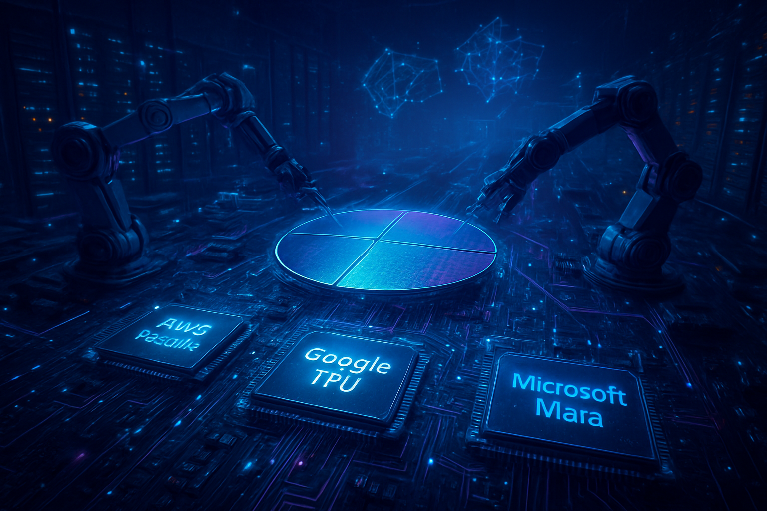
The Rise of Custom Architectures: TPU v7, Trainium3, and Maia 200
The technical specifications of the latest custom silicon reveal a narrowing gap between specialized ASICs (Application-Specific Integrated Circuits) and Nvidia’s flagship GPUs. Google’s TPU v7, codenamed "Ironwood," has emerged as a powerhouse in early 2026. Built on a cutting-edge 3nm process, the TPU v7 matches Nvidia’s Blackwell B200 in raw FP8 compute performance, delivering 4.6 PFLOPS. Google has integrated these chips into massive "pods" of 9,216 units, utilizing an Optical Circuit Switch (OCS) that allows the entire cluster to function as a single 42-exaflop supercomputer. Google now reports that over 75% of its Gemini model computations are handled by its internal TPU fleet, a move that has significantly insulated the company from supply chain volatility.
Amazon Web Services (AWS) has followed suit with the general availability of Trainium3, announced at re:Invent 2025. Trainium3 offers a 2x performance boost over its predecessor and is 4x more energy-efficient, serving as the backbone for "Project Rainier," a massive compute cluster dedicated to Anthropic. Meanwhile, Microsoft is ramping up production of its Maia 200 (Braga) chip. While Maia has faced production delays and currently trails Nvidia’s raw power, Microsoft is leveraging its "MX" data format and advanced liquid-cooled infrastructure to optimize the chip for Azure’s specific AI workloads. These custom chips differ from traditional GPUs by stripping away legacy graphics-processing circuitry, focusing entirely on the dense matrix multiplication required for transformer-based models.
Strategic Realignment: Winners, Losers, and the Shadow Giants
This shift toward vertical integration is fundamentally altering the competitive landscape. For the hyperscalers, the strategic advantage is clear: they can now offer AI compute at prices that Nvidia-based competitors cannot match. In early 2026, AWS implemented a 45% price cut on its Nvidia-based instances, a move widely interpreted as a defensive strategy to keep customers within its ecosystem while it scales up its Trainium and Inferentia offerings. This pricing pressure forces a difficult choice for startups and AI labs: pay a premium for the flexibility of Nvidia’s CUDA ecosystem or migrate to custom silicon for significantly lower operational costs.
While Nvidia remains the dominant force with roughly 90% of the data center GPU market, the "shadow winners" of this transition are the silicon design partners. Broadcom (NASDAQ: AVGO) and Marvell (NASDAQ: MRVL) have become the primary enablers of the custom chip revolution. Broadcom’s AI revenue is projected to reach $46 billion in 2026, driven largely by its role in co-designing Google’s TPUs and Meta’s (NASDAQ: META) MTIA chips. These companies provide the essential intellectual property and design expertise that allow software giants to become hardware manufacturers overnight, effectively commoditizing the silicon layer of the AI stack.
The Great Inference Shift and the Sovereignty Dividend
The broader AI landscape is currently defined by a pivot from training to inference. In 2026, an estimated 70% of all AI workloads are inference-related—the process of running a pre-trained model to generate responses. This is where custom silicon truly shines. While training a frontier model still often requires the raw, flexible power of an Nvidia cluster, the repetitive, high-volume nature of inference is perfectly suited for cost-optimized ASICs. Chips like AWS Inferentia and Meta’s MTIA are designed to maximize "tokens per watt," a metric that has become more important than raw FLOPS for companies operating at a global scale.
This development mirrors previous milestones in computing history, such as the transition from mainframes to distributed cloud computing. Just as the cloud allowed companies to move away from expensive, proprietary hardware toward scalable, utility-based services, custom AI silicon is democratizing access to high-scale inference. However, this trend also raises concerns about "ecosystem lock-in." As hyperscalers optimize their software stacks for their own silicon, moving a model from Google Cloud to Azure or AWS becomes increasingly complex, potentially stifling the interoperability that the open-source AI community has fought to maintain.
The Future of Silicon: Nvidia’s Rubin and Hybrid Ecosystems
Looking ahead, the battle for silicon supremacy is only intensifying. In response to the custom chip threat, Nvidia used CES 2026 to launch its "Vera Rubin" architecture. Named after the pioneering astronomer, the Rubin platform utilizes HBM4 memory and a 3nm process to deliver unprecedented efficiency. Nvidia’s strategy is to make its general-purpose GPUs so efficient that the marginal cost savings of custom silicon become negligible for third-party developers. Furthermore, the upcoming Trainium4 from AWS suggests a future of "hybrid environments," featuring support for Nvidia NVLink Fusion. This will allow custom silicon to sit directly inside Nvidia-designed racks, enabling a mix-and-match approach to compute.
Experts predict that the next two years will see a "tiering" of the AI hardware market. High-end frontier model training will likely remain the domain of Nvidia’s most advanced GPUs, while the vast majority of mid-tier training and global inference will migrate to custom ASICs. The challenge for hyperscalers will be to build software ecosystems that can rival Nvidia’s CUDA, which remains the industry standard for AI development. If the cloud giants can simplify the developer experience for their custom chips, Nvidia’s iron grip on the market may finally be loosened.
Conclusion: A New Era of AI Infrastructure
The rise of custom AI silicon represents one of the most significant shifts in the history of computing. We have moved beyond the "gold rush" phase where any available GPU was a precious commodity, into a sophisticated era of specialized, cost-effective infrastructure. The aggressive moves by Amazon, Google, and Microsoft to build their own chips are not just about saving money; they are about securing their future in an AI-driven world where compute is the most valuable resource.
In the coming months, the industry will be watching the deployment of Nvidia’s Rubin architecture and the performance benchmarks of Microsoft’s Maia 200. As the "Silicon Sovereignty" movement matures, the ultimate winners will be the enterprises and developers who can leverage this new diversity of hardware to build more powerful, efficient, and accessible AI applications. The great silicon divorce is underway, and the AI landscape will never be the same.
This content is intended for informational purposes only and represents analysis of current AI developments.
TokenRing AI delivers enterprise-grade solutions for multi-agent AI workflow orchestration, AI-powered development tools, and seamless remote collaboration platforms.
For more information, visit https://www.tokenring.ai/.