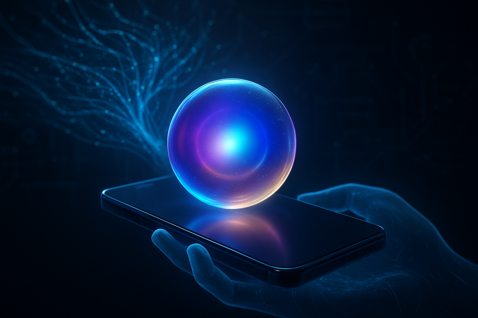
Category: Uncategorized

  • Powering the Cosmos: How Advanced Semiconductors Are Propelling Next-Generation Satellites

    Powering the Cosmos: How Advanced Semiconductors Are Propelling Next-Generation Satellites

    In the vast expanse of space, where extreme conditions challenge even the most robust technology, semiconductors have emerged as the unsung heroes, silently powering the revolution in satellite capabilities. These tiny, yet mighty, components are the bedrock upon which next-generation communication, imaging, and scientific research satellites are built, enabling unprecedented levels of performance, efficiency, and autonomy. As the global space economy expands, fueled by the demand for ubiquitous connectivity and critical Earth observation, the role of advanced semiconductors is becoming ever more critical, transforming our ability to explore, monitor, and connect from orbit.

    The immediate significance of these advancements is profound. We are witnessing the dawn of enhanced global connectivity, with constellations like SpaceX's (NASDAQ: TSLA) Starlink and OneWeb (a subsidiary of Eutelsat Communications S.A. (EPA: ETL)) leveraging these chips to deliver high-speed internet to remote corners of the globe, bridging the digital divide. Earth observation and climate monitoring are becoming more precise and continuous, providing vital data for understanding climate change and predicting natural disasters. Furthermore, radiation-hardened and energy-efficient semiconductors are extending the lifespan and autonomy of spacecraft, allowing for more ambitious and long-duration missions with less human intervention. This miniaturization also leads to more cost-effective space missions, democratizing access to space for a wider array of scientific and commercial endeavors.

    The Microscopic Engines of Orbital Innovation

    The technical prowess behind these next-generation satellites lies in a new breed of semiconductor materials and sophisticated hardening techniques that far surpass the limitations of traditional silicon. Leading the charge are wide-bandgap (WBG) semiconductors like Gallium Nitride (GaN) and Silicon Carbide (SiC), alongside advanced Silicon Germanium (SiGe) alloys.

    GaN, with its wide bandgap of approximately 3.4 eV, offers superior performance in high-frequency and high-power applications. Its high breakdown voltage, exceptional electron mobility, and thermal conductivity make it ideal for RF amplifiers, radar systems, and high-speed communication modules operating in the GHz range. This translates to faster switching speeds, higher power density, and reduced thermal management requirements compared to silicon. SiC, another WBG material with a bandgap of about 3.3 eV, excels in power electronics due to its higher critical electrical field and three times greater thermal conductivity than silicon. SiC devices can operate at temperatures well over 400°C, crucial for power regulation in solar arrays and battery charging in extreme space environments. Both GaN and SiC also boast inherent radiation tolerance, a critical advantage in the harsh cosmic radiation belts.

    Silicon Germanium (SiGe) alloys offer a different set of benefits, particularly in radiation tolerance and high-frequency performance. SiGe heterojunction bipolar transistors (HBTs) can withstand Total Ionizing Dose (TID) levels exceeding 1 Mrad(Si), making them highly resistant to radiation-induced failures. They also operate stably across a broad temperature range, from cryogenic conditions to over 200°C, and achieve cutoff frequencies above 300 GHz, essential for advanced space communication systems. These properties enable increased processing power and efficiency, with SiGe offering four times faster carrier mobility than silicon.

    Radiation hardening, a multifaceted approach, is paramount for ensuring the longevity and reliability of these components. Techniques range from "rad-hard by design" (inherently resilient circuit architectures, error-correcting memory) and "rad-hard by processing" (using insulating substrates like Silicon-on-Insulator (SOI) and specialized materials) to "rad-hard by packaging" (physical shielding with heavy metals). These methods collectively mitigate the effects of cosmic rays, solar flares, and trapped radiation, which can otherwise cause data corruption or catastrophic system failures. Unlike previous silicon-centric approaches that required extensive external shielding, these advanced materials offer intrinsic radiation resistance, leading to lighter, more compact, and more efficient systems.

    The AI research community and industry experts have reacted with significant enthusiasm, recognizing these semiconductor advancements as foundational for enabling sophisticated AI capabilities in space. The superior performance, efficiency, and radiation hardness are critical for deploying complex AI models directly on spacecraft, allowing for real-time decision-making, onboard data processing, and autonomous operations that reduce latency and dependence on Earth-based systems. Experts foresee a "beyond silicon" era where these next-gen semiconductors power more intelligent AI models and high-performance computing (HPC), even exploring in-space manufacturing of semiconductors to produce purer, higher-quality materials.

    Reshaping the Tech Landscape: Benefits, Battles, and Breakthroughs

    The proliferation of advanced semiconductors in space technology is creating ripples across the entire tech industry, offering immense opportunities for semiconductor manufacturers, tech giants, and innovative startups, while also intensifying competitive dynamics.

    Semiconductor manufacturers are at the forefront of this boom. Companies like Advanced Micro Devices (NASDAQ: AMD), Texas Instruments (NASDAQ: TXN), Infineon Technologies AG (ETR: IFX), Microchip Technology (NASDAQ: MCHP), STMicroelectronics N.V. (NYSE: STM), and Teledyne Technologies (NYSE: TDY) are heavily invested in developing radiation-hardened and radiation-tolerant chips, FPGAs, and SoCs tailored for space applications. AMD, for instance, is pushing its Versal Adaptive SoCs, which integrate AI capabilities for on-board inferencing in a radiation-tolerant form factor. AI chip developers like BrainChip Holdings Ltd (ASX: BRN), with its neuromorphic Akida IP, are designing energy-efficient AI solutions specifically for in-orbit processing.

    Tech giants with significant aerospace and defense divisions, such as Lockheed Martin (NYSE: LMT), The Boeing Company (NYSE: BA), and Northrop Grumman Corporation (NYSE: NOC), are major beneficiaries, integrating these advanced semiconductors into their satellite systems and spacecraft. Furthermore, cloud computing leaders and satellite operators like SpaceX (NASDAQ: TSLA) are leveraging these chips for their rapidly expanding constellations, extending global internet coverage and data services. This creates new avenues for tech giants to expand their cloud infrastructure beyond terrestrial boundaries.

    Startups are also finding fertile ground in this specialized market. Companies like AImotive are adapting automotive AI chips for cost-effective Low Earth Orbit (LEO) satellites. More ambitiously, innovative ventures such as Besxar Space Industries and Space Forge are exploring and actively developing in-space manufacturing platforms for semiconductors, aiming to leverage microgravity to produce higher-quality wafers with fewer defects. This burgeoning ecosystem, fueled by increasing government and private investment, indicates a robust environment for new entrants.

    The competitive landscape is marked by significant R&D investment in radiation hardening, miniaturization, and power efficiency. Strategic partnerships between chipmakers, aerospace contractors, and government agencies are becoming crucial for accelerating innovation and market penetration. Vertical integration, where companies control key stages of production, is also a growing trend to ensure supply chain robustness. The specialized nature of space-grade components, with their distinct supply chains and rigorous testing, could also disrupt existing commercial semiconductor supply chains by diverting resources or creating new, space-specific manufacturing paradigms. Ultimately, companies that specialize in radiation-hardened solutions, demonstrate expertise in AI integration for autonomous space systems, and offer highly miniaturized, power-efficient packages will gain significant strategic advantages.

    Beyond Earth's Grasp: Broader Implications and Future Horizons

    The integration of advanced semiconductors and AI in space technology is not merely an incremental improvement; it represents a paradigm shift with profound wider significance, influencing the broader AI landscape, societal well-being, environmental concerns, and geopolitical dynamics.

    This technological convergence fits seamlessly into the broader AI landscape, acting as a crucial enabler for "AI at the Edge" in the most extreme environment imaginable. The demand for specialized hardware to support complex AI algorithms, including large language models and generative AI, is driving innovation in semiconductor design, creating a virtuous cycle where AI helps design better chips, which in turn enable more powerful AI. This extends beyond space, influencing heterogeneous computing, 3D chip stacking, and silicon photonics for faster, more energy-efficient data processing across various sectors.

    The societal impacts are largely positive, promising enhanced global connectivity, improved Earth observation for climate monitoring and disaster management, and advancements in navigation and autonomous systems for deep space exploration. For example, AI-powered systems on satellites can perform real-time cloud masking or identify natural disasters, significantly improving response times. However, there are notable concerns. The manufacturing of semiconductors is resource-intensive, consuming vast amounts of energy and water, and generating greenhouse gas emissions. More critically, the exponential growth in satellite launches, driven by these advancements, exacerbates the problem of space debris. The "Kessler Syndrome" – a cascade of collisions creating more debris – threatens active satellites and could render parts of orbit unusable, impacting essential services and leading to significant financial losses.

    Geopolitical implications are also significant. Advanced semiconductors and AI in space are at the nexus of international competition, particularly between global powers. Control over these technologies is central to national security and military strategies, leading to concerns about an arms race in space, increased military applications of AI-powered systems, and technological sovereignty. Nations are investing heavily in domestic semiconductor production and imposing export controls, disrupting global supply chains and fostering "techno-nationalism." The increasing autonomy of AI in space also raises profound ethical questions regarding data privacy, decision-making without human oversight, and accountability for AI-driven actions, straining existing international space law treaties.

    Comparing this era to previous milestones, the current advancements represent a significant leap from early space semiconductors, which focused primarily on material purity. Today's chips integrate powerful processing capabilities, radiation hardening, miniaturization, and energy efficiency, allowing for complex AI algorithms to run on-board – a stark contrast to the simpler classical computer vision algorithms of past missions. This echoes the Cold War space race in its competitive intensity but is characterized by a "digital cold war" focused on technological decoupling and strategic rivalry over critical supply chains, a shift from overt military and political competition. The current dramatic fall in launch costs, driven by reusable rockets, further democratizes access to space, leading to an explosion in satellite deployment unprecedented in scale.

    The Horizon of Innovation: What Comes Next

    The trajectory for semiconductors in space technology points towards continuous, rapid innovation, promising even more robust, efficient, and intelligent electronics to power future space exploration and commercialization.

    In the near term, we can expect relentless focus on refining radiation hardening techniques, making components inherently more resilient through advanced design, processing, and even software-based approaches. Miniaturization and power efficiency will remain paramount, with the development of more integrated System-on-a-Chip (SoC) solutions and Field-Programmable Gate Arrays (FPGAs) that pack greater computational power into smaller, lighter, and more energy-frugal packages. The adoption of new wide-bandgap materials like GaN and SiC will continue to expand beyond niche applications, becoming core to power architectures due to their superior efficiency and thermal resilience.

    Looking further ahead, the long-term vision includes widespread adoption of advanced packaging technologies like chiplets and 3D integrated circuits (3D ICs) to achieve unprecedented transistor density and performance, pushing past traditional Moore's Law scaling limits. The pursuit of smaller process nodes, such as 3nm and 2nm technologies, will continue to drive performance and energy efficiency. A truly revolutionary prospect is the in-space manufacturing of semiconductors, leveraging microgravity to produce higher-quality wafers with fewer defects, potentially transforming global chip supply chains and enabling novel architectures unachievable on Earth.

    These future developments will unlock a plethora of new applications. We will see even larger, more sophisticated satellite constellations providing ubiquitous connectivity, enhanced Earth observation, and advanced navigation. Deep space exploration and lunar missions will benefit from highly autonomous spacecraft equipped with AI-optimized chips for real-time decision-making and data processing at the "edge," reducing reliance on Earth-based communication. The realm of quantum computing and cryptography in space will also expand, promising breakthroughs in secure communication, ultra-fast problem-solving, and precise quantum navigation. Experts predict the global space semiconductor market, estimated at USD 3.90 billion in 2024, will reach approximately USD 6.65 billion by 2034, with North America leading the growth.

    However, significant challenges remain. The extreme conditions of radiation, temperature fluctuations, and vacuum in space demand components that are incredibly robust, making manufacturing complex and expensive. The specialized nature of space-grade chips often leads to a technological lag compared to commercial counterparts. Moreover, managing power efficiency and thermal dissipation in densely packed, resource-constrained spacecraft will always be a critical engineering hurdle. Geopolitical influences on supply chains, including trade restrictions and the push for technological sovereignty, will continue to shape the industry, potentially driving more onshoring of semiconductor design and manufacturing.

    A New Era of Space Exploration and Innovation

    The journey of semiconductors in space technology is a testament to human ingenuity, pushing the boundaries of what is possible in the most demanding environment. From enabling global internet access to powering autonomous rovers on distant planets, these tiny components are the invisible force behind a new era of space exploration and commercialization.

    The key takeaways are clear: advanced semiconductors, particularly wide-bandgap materials and radiation-hardened designs, are indispensable for next-generation satellite capabilities. They are democratizing access to space, revolutionizing Earth observation, and fundamentally enabling sophisticated AI to operate autonomously in orbit. This development is not just a technological feat but a significant milestone in AI history, marking a pivotal shift towards intelligent, self-sufficient space systems.

    In the coming weeks and months, watch for continued breakthroughs in material science, further integration of AI into onboard processing units, and potentially, early demonstrations of in-space semiconductor manufacturing. The ongoing competitive dynamics, particularly between major global powers, will also dictate the pace and direction of innovation, with a strong emphasis on supply chain resilience and technological sovereignty. As we look to the stars, it's the microscopic marvels within our spacecraft that are truly paving the way for our grandest cosmic ambitions.


    This content is intended for informational purposes only and represents analysis of current AI developments.

    TokenRing AI delivers enterprise-grade solutions for multi-agent AI workflow orchestration, AI-powered development tools, and seamless remote collaboration platforms.
    For more information, visit https://www.tokenring.ai/.

  • The Silicon Brain: How Specialized Chipsets Are Driving Automotive’s Intelligent Revolution

    The Silicon Brain: How Specialized Chipsets Are Driving Automotive’s Intelligent Revolution

    The automotive industry is undergoing a profound transformation, rapidly evolving from a mechanical domain into a sophisticated, software-defined ecosystem where vehicles function as "computers on wheels." At the heart of this revolution lies the escalating integration of specialized chipsets. These advanced semiconductors are no longer mere components but the central nervous system of modern automobiles, enabling a vast array of innovations in safety, performance, connectivity, and user experience. The immediate significance of this trend is its critical role in facilitating next-generation automotive technologies, from extending the range and safety of electric vehicles to making autonomous driving a reality and delivering immersive in-car digital experiences. The increasing demand for these highly reliable and robust semiconductor components highlights their pivotal role in defining the future landscape of mobility, with the global automotive chip market projected for substantial growth in the coming years.

    The Micro-Engineers Behind Automotive Innovation

    The push for smarter, safer, and more connected vehicles has necessitated a departure from general-purpose computing in favor of highly specialized silicon. These purpose-built chipsets are designed to manage the immense data flows and complex algorithms required for cutting-edge automotive functions.

    In Battery Management Systems (BMS) for electric vehicles (EVs), specialized chipsets are indispensable for safe, efficient, and optimized operation. Acting as a "battery nanny," BMS chips meticulously monitor and control rechargeable batteries, performing crucial functions such as precise voltage and current monitoring, temperature sensing, and estimation of the battery's state of charge (SOC) and state of health (SOH). They also manage cell balancing, vital for extending battery life and overall pack performance. These chips enable critical safety features by detecting faults and protecting against overcharge, over-discharge, and thermal runaway. Companies like NXP Semiconductors (NASDAQ: NXPI) and Infineon (XTRA: IFX) are developing advanced BMS chipsets that integrate monitoring, balancing, and protection functionalities, supporting high-voltage applications and meeting stringent safety standards up to ASIL-D.

    Autonomous driving (AD) technology is fundamentally powered by highly specialized AI chips, which serve as the "brain" orchestrating complex real-time operations. These processors handle the massive amounts of data generated by various sensors—cameras, LiDAR, radar, and ultrasound—enabling vehicles to perceive their environment accurately. Specialized AI chips are crucial for processing these inputs, performing sensor fusion, and executing complex AI algorithms for object detection, path planning, and real-time decision-making. For higher levels of autonomy (Level 3 to Level 5), the demand for processing power intensifies, necessitating advanced System-on-Chip (SoC) architectures that integrate AI accelerators, GPUs, and CPUs. Key players include NVIDIA (NASDAQ: NVDA) with its Thor and Orin platforms, Mobileye (NASDAQ: MBLY) with its EyeQ Ultra, Qualcomm (NASDAQ: QCOM) with Snapdragon Ride, and even automakers like Tesla (NASDAQ: TSLA), which designs its custom FSD hardware.

    For in-car entertainment (ICE) and infotainment systems, specialized chipsets play a pivotal role in creating a personalized and connected driving experience. Automotive infotainment SoCs are specifically engineered for managing display audio, navigation, and various in-cabin applications. These chipsets facilitate features such as enhanced connectivity, in-vehicle GPS with real-time mapping, multimedia playback, and intuitive user interfaces. They enable seamless smartphone integration, voice command recognition, and access to digital services. The demand for fast boot times and immediate wake-up from sleep mode is a crucial consideration, ensuring a responsive and user-friendly experience. Manufacturers like STMicroelectronics (NYSE: STM) and MediaTek (TPE: 2454) provide cutting-edge chipsets that power these advanced entertainment and connectivity features.

    Corporate Chessboard: Beneficiaries and Disruptors

    The increasing importance of specialized automotive chipsets is profoundly reshaping the landscape for AI companies, tech giants, and startups, driving innovation, fierce competition, and significant strategic shifts across the industry.

    AI chip startups are at the forefront of designing purpose-built hardware for AI workloads. Companies like Groq, Cerebras Systems, Blaize, and Hailo are developing specialized processors optimized for speed, efficiency, and specific AI models, including transformers essential for large language models (LLMs). These innovations are enabling generative AI capabilities to run directly on edge devices like automotive infotainment systems. Simultaneously, tech giants are leveraging their resources to develop custom silicon and secure supply chains. NVIDIA (NASDAQ: NVDA) remains a leader in AI computing, expanding its influence in automotive AI. AMD (NASDAQ: AMD), with its acquisition of Xilinx, offers FPGA solutions and CPU processors for edge computing. Intel (NASDAQ: INTC), through its Intel Foundry services, is poised to benefit from increased chip demand. Hyperscale cloud providers like Google (NASDAQ: GOOGL), Microsoft (NASDAQ: MSFT), and Amazon (NASDAQ: AMZN) are also developing custom ASICs (e.g., Google's TPUs) to optimize their cloud AI workloads, reduce operational costs, and offer differentiated AI services. Samsung (KRX: 005930) benefits from its foundry business, exemplified by its deal to produce Tesla's next-generation AI6 automotive chips.

    Automotive OEMs are embracing vertical integration or collaboration. Tesla (NASDAQ: TSLA) designs its own chips and controls its hardware and software stack, offering streamlined development and better performance. European OEMs like Stellantis (NYSE: STLA), Mercedes-Benz (ETR: MBG), and Volkswagen (OTC: VWAGY) are adopting collaborative, platform-centric approaches to accelerate the development of software-defined vehicles (SDVs). Traditional automotive suppliers like NXP Semiconductors (NASDAQ: NXPI) and Bosch are also actively developing AI-driven solutions for automated driving and electrification. Crucially, TSMC (NYSE: TSM), as the world's largest outsourced semiconductor foundry, is a primary beneficiary, manufacturing high-end AI chipsets for major tech companies.

    This intense competition is driving a "AI chip arms race," leading to diversification of hardware supply chains, where major AI labs seek to reduce reliance on single-source suppliers. Tech giants are pursuing strategic independence through custom silicon, disrupting traditional cloud AI services. Chipmakers are evolving from mere hardware suppliers to comprehensive solution providers, expanding their software capabilities. The rise of specialized chipsets is also disrupting the traditional automotive business model, shifting towards revenue generation from software upgrades and services delivered via over-the-air (OTA) updates. This redefines power dynamics, potentially elevating tech giants while challenging traditional car manufacturers to adapt or risk being relegated to hardware suppliers.

    Beyond the Dashboard: Wider Significance and Concerns

    The integration of specialized automotive chipsets is a microcosm of a broader "AI supercycle" that is reshaping the semiconductor industry and the entire technological landscape. This trend signifies a diversification and customization of AI chips, driven by the imperative for enhanced performance, greater energy efficiency, and the widespread enablement of edge computing. This "hardware renaissance" is making advanced AI more accessible, sustainable, and powerful across various sectors, with the global AI chip market projected to reach $460.9 billion by 2034.

    Beyond the automotive sector, these advancements are driving industrial transformation in healthcare, robotics, natural language processing, and scientific research. The demand for low-power, high-efficiency NPUs, initially propelled by automotive needs, is transforming other edge AI devices like industrial robotics, smart cameras, and AI-enabled PCs. This enables real-time decision-making, enhanced privacy, and reduced reliance on cloud resources. The semiconductor industry is evolving, with players shifting from hardware suppliers to solution providers. The increased reliance on specialized chipsets is also part of a larger trend towards software-defined everything, meaning more functionality is determined by software running on powerful, specialized hardware, opening new avenues for updates, customization, and new business models. Furthermore, the push for energy-efficient chips in automotive applications translates into broader efforts to reduce the significant energy demands of AI workloads.

    However, this rapid evolution brings potential concerns. The reliance on specialized chipsets exacerbates existing supply chain vulnerabilities, as evidenced by past chip shortages that caused production delays. The high development and manufacturing costs of cutting-edge AI chips pose a significant barrier, potentially concentrating power among a few large corporations and driving up vehicle costs. Ethical implications include data privacy and security, as AI chipsets gather vast amounts of vehicular data. The transparency of AI decision-making in autonomous vehicles is crucial for accountability. There are also concerns about potential job displacement due to automation and the risk of algorithmic bias if training data is flawed. The complexity of integrating diverse specialized chips can lead to hardware fragmentation and interoperability challenges.

    Compared to previous AI milestones, the current trend of specialized automotive chipsets represents a further refinement beyond the shift from CPUs to GPUs for AI workloads. It signifies a move to even more tailored solutions like ASICs and NPUs, analogous to how AI's specialized demands moved beyond general-purpose CPUs and now beyond general-purpose GPUs to achieve optimal performance and efficiency, especially with the rise of generative AI. This "hardware renaissance" is not just making existing AI faster but fundamentally expanding what AI can achieve, paving the way for more powerful, pervasive, and sustainable intelligent systems.

    The Road Ahead: Future Developments

    The future of specialized automotive chipsets is characterized by unprecedented growth and innovation, fundamentally reshaping vehicles into intelligent, connected, and autonomous systems.

    In the near term (next 1-5 years), we can expect enhanced ADAS capabilities, driven by chips that process real-time sensor data more effectively. The integration of 5G-capable chipsets will become essential for Vehicle-to-Everything (V2X) communication and edge computing, ensuring faster and safer decision-making. AI and machine learning integration will deepen, requiring more sophisticated processing units for object detection, movement prediction, and traffic management. For EVs, power management innovations will focus on maximizing energy efficiency and optimizing battery performance. We will also see a rise in heterogeneous systems and chiplet technology to manage increasing complexity and performance demands.

    Long-term advancements (beyond 5 years) will push towards higher levels of autonomous driving (L4/L5), demanding exponentially faster and more capable chips, potentially rivaling today's supercomputers. Neuromorphic chips, designed to mimic the human brain, offer real-time decision-making with significantly lower power consumption, ideal for self-driving cars. Advanced in-cabin user experiences will include augmented reality (AR) heads-up displays, sophisticated in-car gaming, and advanced conversational voice interfaces powered by LLMs. Breakthroughs are anticipated in new materials like graphene and wide bandgap semiconductors (SiC, GaN) for power electronics. The concept of Software-Defined Vehicles (SDVs) will fully mature, where vehicle controls are primarily managed by software, offering continuous updates and customizable experiences.

    These chipsets will enable a wide array of applications, from advanced sensor fusion for autonomous driving to enhanced V2X connectivity for intelligent traffic management. They will power sophisticated infotainment systems, optimize electric powertrains, and enhance active safety systems.

    However, significant challenges remain. The immense complexity of modern vehicles, with over 100 Electronic Control Units (ECUs) and millions of lines of code, makes verification and integration difficult. Security is a growing concern as connected vehicles present a larger attack surface for cyber threats, necessitating robust encryption and continuous monitoring. A lack of unified standardization for rapidly changing automotive systems, especially concerning cybersecurity, poses difficulties. Supply chain resilience remains a critical issue, pushing automakers towards vertical integration or long-term partnerships. The high R&D investment for new chips, coupled with relatively smaller automotive market volumes compared to consumer electronics, also presents a challenge.

    Experts predict significant market growth, with the automotive semiconductor market forecast to double to $132 billion by 2030. The average semiconductor content per vehicle is expected to grow, with EVs requiring three times more semiconductors than internal combustion engine (ICE) vehicles. The shift to software-defined platforms and the mainstreaming of Level 2 automation are also key predictions.

    The Intelligent Journey: A Comprehensive Wrap-Up

    The rapid evolution of specialized automotive chipsets stands as a pivotal development in the ongoing transformation of the automotive industry, heralding an era of unprecedented innovation in vehicle intelligence, safety, and connectivity. These advanced silicon solutions are no longer mere components but the "digital heart" of modern vehicles, underpinning a future where cars are increasingly smart, autonomous, and integrated into a broader digital ecosystem.

    The key takeaway is that specialized chipsets are indispensable for enabling advanced driver-assistance systems, fully autonomous driving, sophisticated in-vehicle infotainment, and seamless connected car ecosystems. The market is experiencing robust growth, driven by the increasing deployment of autonomous and semi-autonomous vehicles and the imperative for real-time data processing. This progression showcases AI's transition from theoretical concepts to becoming an embedded, indispensable component of safety-critical and highly complex machines.

    The long-term impact will be profound, fundamentally redefining personal and public transportation. We can anticipate transformative mobility through safer roads and more efficient traffic management, with SDVs becoming the standard, allowing for continuous OTA updates and personalized experiences. This will drive significant economic shifts and further strategic partnerships within the automotive supply chain. Continuous innovation in energy-efficient AI processors and neuromorphic computing will be crucial, alongside the development of robust ethical guidelines and harmonized regulatory standards.

    In the coming weeks and months, watch for continued advancements in chiplet technology, increased NPU integration for advanced AI tasks, and enhanced edge AI capabilities to minimize latency. Strategic collaborations between automakers and semiconductor companies will intensify to fortify supply chains. Keep an eye on progress towards higher levels of autonomy and the wider adoption of 5G and V2X communication, which will collectively underscore the foundational role of specialized automotive chipsets in driving the next wave of automotive innovation.


    This content is intended for informational purposes only and represents analysis of current AI developments.

    TokenRing AI delivers enterprise-grade solutions for multi-agent AI workflow orchestration, AI-powered development tools, and seamless remote collaboration platforms.
    For more information, visit https://www.tokenring.ai/.

  • The 2-Nanometer Frontier: A Global Race to Reshape AI and Computing

    The 2-Nanometer Frontier: A Global Race to Reshape AI and Computing

    The semiconductor industry is currently embroiled in an intense global race to develop and mass-produce advanced 2-nanometer (nm) chips, pushing the very boundaries of miniaturization and performance. This pursuit represents a pivotal moment for technology, promising unprecedented advancements that will redefine computing capabilities across nearly every sector. These next-generation chips are poised to deliver revolutionary improvements in processing speed and energy efficiency, allowing for significantly more powerful and compact devices.

    The immediate significance of 2nm chips is profound. Prototypes, such as IBM's groundbreaking 2nm chip, project an astonishing 45% higher performance or 75% lower energy consumption compared to current 7nm chips. Similarly, Taiwan Semiconductor Manufacturing Company (TSMC) (NYSE: TSM) aims for a 10-15% performance boost and a 25-30% reduction in power consumption over its 3nm predecessors. This leap in efficiency and power directly translates to longer battery life for mobile devices, faster processing for AI workloads, and a reduced carbon footprint for data centers. Moreover, the smaller 2nm process allows for an exponential increase in transistor density, with designs like IBM's capable of fitting up to 50 billion transistors on a chip the size of a fingernail, ensuring the continued march of Moore's Law. This miniaturization is crucial for accelerating advancements in artificial intelligence (AI), high-performance computing (HPC), autonomous vehicles, 5G/6G communication, and the Internet of Things (IoT).

    The Technical Leap: Gate-All-Around and Beyond

    The transition to 2nm technology is fundamentally driven by a significant architectural shift in transistor design. For years, the industry relied on FinFET (Fin Field-Effect Transistor) architecture, but at 2nm and beyond, FinFETs face physical limitations in controlling current leakage and maintaining performance. The key technological advancement enabling 2nm is the widespread adoption of Gate-All-Around (GAA) transistor architecture, often implemented as nanosheet or nanowire FETs. This innovative design allows the gate to completely surround the channel, providing superior electrostatic control, which significantly reduces leakage current and enhances performance at smaller scales.

    Leading the charge in this technical evolution are industry giants like TSMC, Samsung (KRX: 005930), and Intel (NASDAQ: INTC). TSMC's N2 process, set for mass production in the second half of 2025, is its first to fully embrace GAA. Samsung, a fierce competitor, was an early adopter of GAA for its 3nm chips and is "all-in" on the technology for its 2nm process, slated for production in 2025. Intel, with its aggressive 18A (1.8nm-class) process, incorporates its own version of GAAFETs, dubbed RibbonFET, alongside a novel power delivery system called PowerVia, which moves power lines to the backside of the wafer to free up space on the front for more signal routing. These innovations are critical for achieving the density and performance targets of the 2nm node.

    The technical specifications of these 2nm chips are staggering. Beyond raw performance and power efficiency gains, the increased transistor density allows for more complex and specialized logic circuits to be integrated directly onto the chip. This is particularly beneficial for AI accelerators, enabling more sophisticated neural network architectures and on-device AI processing. Initial reactions from the AI research community and industry experts have been overwhelmingly positive, marked by intense demand. TSMC has reported promising early yields for its N2 process, estimated between 60% and 70%, and its 2nm production capacity for 2026 is already fully booked, with Apple (NASDAQ: AAPL) reportedly reserving over half of the initial output for its future iPhones and Macs. This high demand underscores the industry's belief that 2nm chips are not just an incremental upgrade, but a foundational technology for the next wave of innovation, especially in AI. The economic and geopolitical importance of mastering this technology cannot be overstated, as nations invest heavily to secure domestic semiconductor production capabilities.

    Competitive Implications and Market Disruption

    The global race for 2-nanometer chips is creating a highly competitive landscape, with significant implications for AI companies, tech giants, and startups alike. The foundries that successfully achieve high-volume, high-yield 2nm production stand to gain immense strategic advantages, dictating the pace of innovation for their customers. TSMC, with its reported superior early yields and fully booked 2nm capacity for 2026, appears to be in a commanding position, solidifying its role as the primary enabler for many of the world's leading AI and tech companies. Companies like Apple, AMD (NASDAQ: AMD), NVIDIA (NASDAQ: NVDA), and Qualcomm (NASDAQ: QCOM) are deeply reliant on these advanced nodes for their next-generation products, making access to TSMC's 2nm capacity a critical competitive differentiator.

    Samsung is aggressively pursuing its 2nm roadmap, aiming to catch up and even surpass TSMC. Its "all-in" strategy on GAA technology and significant deals, such as the reported $16.5 billion agreement with Tesla (NASDAQ: TSLA) for 2nm chips, indicate its determination to secure a substantial share of the high-end foundry market. If Samsung can consistently improve its yield rates, it could offer a crucial alternative sourcing option for companies looking to diversify their supply chains or gain a competitive edge. Intel, with its ambitious 18A process, is not only aiming to reclaim its manufacturing leadership but also to become a major foundry for external customers. Its recent announcement of mass production for 18A chips in October 2025, claiming to be ahead of some competitors in this class, signals a serious intent to disrupt the foundry market. The success of Intel Foundry Services (IFS) in attracting major clients will be a key factor in its resurgence.

    The availability of 2nm chips will profoundly disrupt existing products and services. For AI, the enhanced performance and efficiency mean that more complex models can run faster, both in data centers and on edge devices. This could lead to a new generation of AI-powered applications that were previously computationally infeasible. Startups focusing on advanced AI hardware or highly optimized AI software stand to benefit immensely, as they can leverage these powerful new chips to bring their innovative solutions to market. However, companies reliant on older process nodes may find their products quickly becoming obsolete, facing pressure to adopt the latest technology or risk falling behind. The immense cost of 2nm chip development and production also means that only the largest and most well-funded companies can afford to design and utilize these cutting-edge components, potentially widening the gap between tech giants and smaller players, unless innovative ways to access these technologies emerge.

    Wider Significance in the AI Landscape

    The advent of 2-nanometer chips represents a monumental stride that will profoundly reshape the broader AI landscape and accelerate prevailing technological trends. At its core, this miniaturization and performance boost directly fuels the insatiable demand for computational power required by increasingly complex AI models, particularly in areas like large language models (LLMs), generative AI, and advanced machine learning. These chips will enable faster training of models, more efficient inference at scale, and the proliferation of on-device AI capabilities, moving intelligence closer to the data source and reducing latency. This fits perfectly into the trend of pervasive AI, where AI is integrated into every aspect of computing, from cloud servers to personal devices.

    The impacts of 2nm chips are far-reaching. In AI, they will unlock new levels of performance for real-time processing in autonomous systems, enhance the capabilities of AI-driven scientific discovery, and make advanced AI more accessible and energy-efficient for a wider array of applications. For instance, the ability to run sophisticated AI algorithms directly on a smartphone or in an autonomous vehicle without constant cloud connectivity opens up new paradigms for privacy, security, and responsiveness. Potential concerns, however, include the escalating cost of developing and manufacturing these cutting-edge chips, which could further centralize power among a few dominant foundries and chip designers. There are also environmental considerations regarding the energy consumption of fabrication plants and the lifecycle of these increasingly complex devices.

    Comparing this milestone to previous AI breakthroughs, the 2nm chip race is analogous to the foundational leaps in transistor technology that enabled the personal computer revolution or the rise of the internet. Just as those advancements provided the hardware bedrock for subsequent software innovations, 2nm chips will serve as the crucial infrastructure for the next generation of AI. They promise to move AI beyond its current capabilities, allowing for more human-like reasoning, more robust decision-making in real-world scenarios, and the development of truly intelligent agents. This is not merely an incremental improvement but a foundational shift that will underpin the next decade of AI progress, facilitating advancements in areas from personalized medicine to climate modeling.

    The Road Ahead: Future Developments and Challenges

    The immediate future will see the ramp-up of 2nm mass production from TSMC, Samsung, and Intel throughout 2025 and into 2026. Experts predict a fierce battle for market share, with each foundry striving to optimize yields and secure long-term contracts with key customers. Near-term developments will focus on integrating these chips into flagship products: Apple's next-generation iPhones and Macs, new high-performance computing platforms from AMD and NVIDIA, and advanced mobile processors from Qualcomm and MediaTek. The initial applications will primarily target high-end consumer electronics, data center AI accelerators, and specialized components for autonomous driving and advanced networking.

    Looking further ahead, the pursuit of even smaller nodes, such as 1.4nm (often referred to as A14) and potentially 1nm, is already underway. Challenges that need to be addressed include the increasing complexity and cost of manufacturing, which demands ever more sophisticated Extreme Ultraviolet (EUV) lithography machines and advanced materials science. The physical limits of silicon-based transistors are also becoming apparent, prompting research into alternative materials and novel computing paradigms like quantum computing or neuromorphic chips. Experts predict that while silicon will remain dominant for the foreseeable future, hybrid approaches and new architectures will become increasingly important to continue the trajectory of performance improvements. The integration of specialized AI accelerators directly onto the chip, designed for specific AI workloads, will also become more prevalent.

    What experts predict will happen next is a continued specialization of chip design. Instead of a one-size-fits-all approach, we will see highly customized chips optimized for specific AI tasks, leveraging the increased transistor density of 2nm and beyond. This will lead to more efficient and powerful AI systems tailored for everything from edge inference in IoT devices to massive cloud-based training of foundation models. The geopolitical implications will also intensify, as nations recognize the strategic importance of domestic chip manufacturing capabilities, leading to further investments and potential trade policy shifts. The coming years will be defined by how successfully the industry navigates these technical, economic, and geopolitical challenges to fully harness the potential of 2nm technology.

    A New Era of Computing: Wrap-Up

    The global race to produce 2-nanometer chips marks a monumental inflection point in the history of technology, heralding a new era of unprecedented computing power and efficiency. The key takeaways from this intense competition are the critical shift to Gate-All-Around (GAA) transistor architecture, the staggering performance and power efficiency gains promised by these chips, and the fierce competition among TSMC, Samsung, and Intel to lead this technological frontier. These advancements are not merely incremental; they are foundational, providing the essential hardware bedrock for the next generation of artificial intelligence, high-performance computing, and ubiquitous smart devices.

    This development's significance in AI history cannot be overstated. Just as earlier chip advancements enabled the rise of deep learning, 2nm chips will unlock new paradigms for AI, allowing for more complex models, faster training, and pervasive on-device intelligence. They will accelerate the development of truly autonomous systems, more sophisticated generative AI, and AI-driven solutions across science, medicine, and industry. The long-term impact will be a world where AI is more deeply integrated, more powerful, and more energy-efficient, driving innovation across every sector.

    In the coming weeks and months, industry observers should watch for updates on yield rates from the major foundries, announcements of new design wins for 2nm processes, and the first wave of consumer and enterprise products incorporating these cutting-edge chips. The strategic positioning of Intel Foundry Services, the continued expansion plans of TSMC and Samsung, and the emergence of new players like Rapidus will also be crucial indicators of the future trajectory of the semiconductor industry. The 2nm frontier is not just about smaller chips; it's about building the fundamental infrastructure for a smarter, more connected, and more capable future powered by advanced AI.


    This content is intended for informational purposes only and represents analysis of current AI developments.

    TokenRing AI delivers enterprise-grade solutions for multi-agent AI workflow orchestration, AI-powered development tools, and seamless remote collaboration platforms.
    For more information, visit https://www.tokenring.ai/.

  • Micron Surges as AI Ignites a New Memory Chip Supercycle

    Micron Surges as AI Ignites a New Memory Chip Supercycle

    Micron Technology (NASDAQ: MU) is currently experiencing an unprecedented surge in its stock performance, reflecting a profound shift in the semiconductor sector, particularly within the memory chip market. As of late October 2025, the company's shares have not only reached all-time highs but have also significantly outpaced broader market indices, with a year-to-date gain of over 166%. This remarkable momentum is largely attributed to Micron's exceptional financial results and, more critically, the insatiable demand for high-bandwidth memory (HBM) driven by the accelerating artificial intelligence (AI) revolution.

    The immediate significance of Micron's ascent extends beyond its balance sheet, signaling a robust and potentially prolonged "super cycle" for the entire memory industry. Investor sentiment is overwhelmingly bullish, as the market recognizes AI's transformative impact on memory chip requirements, pushing both DRAM and NAND prices upwards after a period of oversupply. Micron's strategic pivot towards high-margin, AI-centric products like HBM is positioning it as a pivotal player in the global AI infrastructure build-out, reshaping the competitive landscape for memory manufacturers and influencing the broader technology ecosystem.

    The AI Engine: HBM3E and the Redefinition of Memory Demand

    Micron Technology's recent success is deeply rooted in its strategic technical advancements and its ability to capitalize on the burgeoning demand for specialized memory solutions. A cornerstone of this momentum is the company's High-Bandwidth Memory (HBM) offerings, particularly its HBM3E products. Micron has successfully qualified its HBM3E with NVIDIA (NASDAQ: NVDA) for the "Blackwell" AI accelerator platform and is actively shipping high-volume HBM to four major customers across GPU and ASIC platforms. This advanced memory technology is critical for AI workloads, offering significantly higher bandwidth and lower power consumption compared to traditional DRAM, which is essential for processing the massive datasets required by large language models and other complex AI algorithms.

    The technical specifications of HBM3E represent a significant leap from previous memory architectures. It stacks multiple DRAM dies vertically, connected by through-silicon vias (TSVs), allowing for a much wider data bus and closer proximity to the processing unit. This design dramatically reduces latency and increases data throughput, capabilities that are indispensable for high-performance computing and AI accelerators. Micron's entire 2025 HBM production capacity is already sold out, with bookings extending well into 2026, underscoring the unprecedented demand for this specialized memory. HBM revenue for fiscal Q4 2025 alone approached $2 billion, indicating an annualized run rate of nearly $8 billion.

    This current memory upcycle fundamentally differs from previous cycles, which were often driven by PC or smartphone demand fluctuations. The distinguishing factor now is the structural and persistent demand generated by AI. Unlike traditional commodity memory, HBM commands a premium due to its complexity and critical role in AI infrastructure. This shift has led to an "unprecedented" demand for DRAM from AI, causing prices to surge by 20-30% across the board in recent weeks, with HBM seeing even steeper jumps of 13-18% quarter-over-quarter in Q4 2025. Even the NAND flash market, after nearly two years of price declines, is showing strong signs of recovery, with contract prices expected to rise by 5-10% in Q4 2025, driven by AI and high-capacity applications.

    Initial reactions from the AI research community and industry experts have been overwhelmingly positive, highlighting the critical enabler role of advanced memory in AI's progression. Analysts have upgraded Micron's ratings and raised price targets, recognizing the company's successful pivot. The consensus is that the memory market is entering a new "super cycle" that is less susceptible to the traditional boom-and-bust patterns, given the long-term structural demand from AI. This sentiment is further bolstered by Micron's expectation to achieve HBM market share parity with its overall DRAM share by the second half of 2025, solidifying its position as a key beneficiary of the AI era.

    Ripple Effects: How the Memory Supercycle Reshapes the Tech Landscape

    Micron Technology's (NASDAQ: MU) surging fortunes are emblematic of a profound recalibration across the entire technology sector, driven by the AI-powered memory chip supercycle. While Micron, along with its direct competitors like SK Hynix (KRX: 000660) and Samsung Electronics (KRX: 005930), stands as a primary beneficiary, the ripple effects extend to AI chip developers, major tech giants, and even nascent startups, reshaping competitive dynamics and strategic priorities.

    Other major memory producers are similarly thriving. South Korean giants SK Hynix (KRX: 000660) and Samsung Electronics (KRX: 005930) have also reported record profits and sold-out HBM capacities through 2025 and well into 2026. This intense demand for HBM means that while these companies are enjoying unprecedented revenue and margin growth, they are also aggressively expanding production, which in turn impacts the supply and pricing of conventional DRAM and NAND used in PCs, smartphones, and standard servers. For AI chip developers such as NVIDIA (NASDAQ: NVDA), Advanced Micro Devices (NASDAQ: AMD), and Intel (NASDAQ: INTC), the availability and cost of HBM are critical. NVIDIA, a primary driver of HBM demand, relies heavily on its suppliers to meet the insatiable appetite for its AI accelerators, making memory supply a key determinant of its scaling capabilities and product costs.

    For major AI labs and tech giants like OpenAI, Alphabet (NASDAQ: GOOGL), Amazon (NASDAQ: AMZN), Microsoft (NASDAQ: MSFT), and Meta Platforms (NASDAQ: META), the supercycle presents a dual challenge and opportunity. These companies are the architects of the AI boom, investing billions in infrastructure projects like OpenAI’s "Stargate." However, the rapidly escalating prices and scarcity of HBM translate into significant cost pressures, impacting the margins of their cloud services and the budgets for their AI development. To mitigate this, tech giants are increasingly forging long-term supply agreements with memory manufacturers and intensifying their in-house chip development efforts to gain greater control over their supply chains and optimize for specific AI workloads, as seen with Google’s (NASDAQ: GOOGL) TPUs.

    Startups, while facing higher barriers to entry due to elevated memory costs and limited supply access, are also finding strategic opportunities. The scarcity of HBM is spurring innovation in memory efficiency, alternative architectures like Processing-in-Memory (PIM), and solutions that optimize existing, cheaper memory types. Companies like Enfabrica, backed by NVIDIA (NASDAQ: NVDA), are developing systems that leverage more affordable DDR5 memory to help AI companies scale cost-effectively. This environment fosters a new wave of innovation focused on memory-centric designs and efficient data movement, which could redefine the competitive landscape for AI hardware beyond raw compute power.

    A New Industrial Revolution: Broadening Impacts and Lingering Concerns

    The AI-driven memory chip supercycle, spearheaded by companies like Micron Technology (NASDAQ: MU), signifies far more than a cyclical upturn; it represents a fundamental re-architecture of the global technology landscape, akin to a new industrial revolution. Its impacts reverberate across economic, technological, and societal spheres, while also raising critical concerns about accessibility and sustainability.

    Economically, the supercycle is propelling the semiconductor industry towards unprecedented growth. The global AI memory chip design market, estimated at $110 billion in 2024, is forecast to skyrocket to nearly $1.25 trillion by 2034, exhibiting a staggering compound annual growth rate of 27.50%. This surge is translating into substantial revenue growth for memory suppliers, with conventional DRAM and NAND contract prices projected to see significant increases through late 2025 and into 2026. This financial boom underscores memory's transformation from a commodity to a strategic, high-value component, driving significant capital expenditure and investment in advanced manufacturing facilities, particularly in the U.S. with CHIPS Act funding.

    Technologically, the supercycle highlights a foundational shift where AI advancement is directly bottlenecked and enabled by hardware capabilities, especially memory. High-Bandwidth Memory (HBM), with its 3D-stacked architecture, offers unparalleled low latency and high bandwidth, serving as a "superhighway for data" that allows AI accelerators to operate at their full potential. Innovations are extending beyond HBM to concepts like Compute Express Link (CXL) for in-memory computing, addressing memory disaggregation and latency challenges in next-generation server architectures. Furthermore, AI itself is being leveraged to accelerate chip design and manufacturing, creating a symbiotic relationship where AI both demands and empowers the creation of more advanced semiconductors, with HBM4 memory expected to commercialize in late 2025.

    Societally, the implications are profound, as AI-driven semiconductor advancements spur transformations in healthcare, finance, manufacturing, and autonomous systems. However, this rapid growth also brings critical concerns. The immense power demands of AI systems and data centers are a growing environmental issue, with global AI energy consumption projected to increase tenfold, potentially exceeding Belgium’s annual electricity use by 2026. Semiconductor manufacturing is also highly water-intensive, raising sustainability questions. Furthermore, the rising cost and scarcity of advanced AI resources could exacerbate the digital divide, potentially favoring well-funded tech giants over smaller startups and limiting broader access to cutting-edge AI capabilities. Geopolitical tensions and export restrictions also contribute to supply chain stress and could impact global availability.

    This current AI-driven memory chip supercycle fundamentally differs from previous AI milestones and tech booms. Unlike past cycles driven by broad-based demand for PCs or smartphones, this supercycle is fueled by a deeper, structural shift in how computers are built, with AI inference and training requiring massive and specialized memory infrastructure. Previous breakthroughs focused primarily on processing power; while GPUs remain indispensable, specialized memory is now equally vital for data throughput. This era signifies a departure where memory, particularly HBM, has transitioned from a supporting component to a critical, strategic asset and the central bottleneck for AI advancement, actively enabling new frontiers in AI development. The "memory wall"—the performance gap between processors and memory—remains a critical challenge that necessitates fundamental architectural changes in memory systems, distinguishing this sustained demand from typical 2-3 year market fluctuations.

    The Road Ahead: Memory Innovations Fueling AI's Next Frontier

    The trajectory of AI's future is inextricably linked to the relentless evolution of memory technology. As of late 2025, the industry stands on the cusp of transformative developments in memory architectures that will enable increasingly sophisticated AI models and applications, though significant challenges related to supply, cost, and energy consumption remain.

    In the near term (late 2025-2027), High-Bandwidth Memory (HBM) will continue its critical role. HBM4 is projected for mass production in 2025, promising a 40% increase in bandwidth and a 70% reduction in power consumption compared to HBM3E, with HBM4E following in 2026. This continuous improvement in HBM capacity and efficiency is vital for the escalating demands of AI accelerators. Concurrently, Low-Power Double Data Rate 6 (LPDDR6) is expected to enter mass production by late 2025 or 2026, becoming indispensable for edge AI devices such as smartphones, AR/VR headsets, and autonomous vehicles, enabling high bandwidth at significantly lower power. Compute Express Link (CXL) is also rapidly gaining traction, with CXL 3.0/3.1 enabling memory pooling and disaggregation, allowing CPUs and GPUs to dynamically access a unified memory pool, a powerful capability for complex AI/HPC workloads.

    Looking further ahead (2028 and beyond), the memory roadmap envisions HBM5 by 2029, doubling I/O count and increasing bandwidth to 4 TB/s per stack, with HBM6 projected for 2032 to reach 8 TB/s. Beyond incremental HBM improvements, the long-term future points to revolutionary paradigms like In-Memory Computing (IMC) or Processing-in-Memory (PIM), where computation occurs directly within or very close to memory. This approach promises to drastically reduce data movement, a major bottleneck and energy drain in current architectures. IBM Research, for instance, is actively exploring analog in-memory computing with 3D analog memory architectures and phase-change memory, while new memory technologies like Resistive Random-Access Memory (ReRAM) and Magnetic Random-Access Memory (MRAM) are being developed for their higher density and energy efficiency in IMC applications.

    These advancements will unlock a new generation of AI applications. Hyper-personalization and "infinite memory" AI are on the horizon, allowing AI systems to remember past interactions and context for truly individualized experiences across various sectors. Real-time AI at the edge, powered by LPDDR6 and emerging non-volatile memories, will enable more sophisticated on-device intelligence with low latency. HBM and CXL are essential for scaling Large Language Models (LLMs) and generative AI, accelerating training and reducing inference latency. Experts predict that agentic AI, capable of persistent memory, long-term goals, and multi-step task execution, will become mainstream by 2027-2028, potentially automating entire categories of administrative work.

    However, the path forward is fraught with challenges. A severe global shortage of HBM is expected to persist through 2025 and into 2026, leading to price hikes and potential delays in AI chip shipments. The advanced packaging required for HBM integration, such as TSMC’s (NYSE: TSM) CoWoS, is also a major bottleneck, with demand far exceeding capacity. The high cost of HBM, often accounting for 50-60% of an AI GPU’s manufacturing cost, along with rising prices for conventional memory, presents significant financial hurdles. Furthermore, the immense energy consumption of AI workloads is a critical concern, with memory subsystems alone accounting for up to 50% of total system power. Global AI energy demand is projected to double from 2022 to 2026, posing significant sustainability challenges and driving investments in renewable power and innovative cooling techniques. Experts predict that memory-centric architectures, prioritizing performance per watt, will define the future of sustainable AI infrastructure.

    The Enduring Impact: Micron at the Forefront of AI's Memory Revolution

    Micron Technology's (NASDAQ: MU) extraordinary stock momentum in late 2025 is not merely a fleeting market trend but a definitive indicator of a fundamental and enduring shift in the technology landscape: the AI-driven memory chip supercycle. This period marks a pivotal moment where advanced memory has transitioned from a supporting component to the very bedrock of AI's exponential growth, with Micron strategically positioned at its epicenter.

    Key takeaways from this transformative period include Micron's successful evolution from a historically cyclical memory company to a more stable, high-margin innovator. Its leadership in High-Bandwidth Memory (HBM), particularly the successful qualification and high-volume shipments of HBM3E for critical AI platforms like NVIDIA’s (NASDAQ: NVDA) Blackwell accelerators, has solidified its role as an indispensable enabler of the AI revolution. This strategic pivot, coupled with disciplined supply management, has translated into record revenues and significantly expanded gross margins, signaling a robust comeback and establishing a "structurally higher margin floor" for the company. The overwhelming demand for Micron's HBM, with 2025 capacity sold out and much of 2026 secured through long-term agreements, underscores the sustained nature of this supercycle.

    In the grand tapestry of AI history, this development is profoundly significant. It highlights that the "memory wall"—the performance gap between processors and memory—has become the primary bottleneck for AI advancement, necessitating fundamental architectural changes in memory systems. Micron's ability to innovate and scale HBM production directly supports the exponential growth of AI capabilities, from training massive large language models to enabling real-time inference at the edge. The era where memory was treated as a mere commodity is over; it is now recognized as a critical strategic asset, dictating the pace and potential of artificial intelligence.

    Looking ahead, the long-term impact for Micron and the broader memory industry appears profoundly positive. The AI supercycle is establishing a new paradigm of more stable pricing and higher margins for leading memory manufacturers. Micron's strategic investments in capacity expansion, such as its $7 billion advanced packaging facility in Singapore, and its aggressive development of next-generation HBM4 and HBM4E technologies, position it for sustained growth. The company's focus on high-value products and securing long-term customer agreements further de-risks its business model, promising a more resilient and profitable future.

    In the coming weeks and months, investors and industry observers should closely watch Micron's Q1 Fiscal 2026 earnings report, expected around December 17, 2025, for further insights into its HBM revenue and forward guidance. Updates on HBM capacity ramp-up, especially from its Malaysian, Taichung, and new Hiroshima facilities, will be critical. The competitive dynamics with SK Hynix (KRX: 000660) and Samsung (KRX: 005930) in HBM market share, as well as the progress of HBM4 and HBM4E development, will also be key indicators. Furthermore, the evolving pricing trends for standard DDR5 and NAND flash, and the emerging demand from "Edge AI" devices like AI-enhanced PCs and smartphones from 2026 onwards, will provide crucial insights into the enduring strength and breadth of this transformative memory supercycle.


    This content is intended for informational purposes only and represents analysis of current AI developments.

    TokenRing AI delivers enterprise-grade solutions for multi-agent AI workflow orchestration, AI-powered development tools, and seamless remote collaboration platforms.
    For more information, visit https://www.tokenring.ai/.

  • KLA Corporation: The Unseen Architect Powering the AI Revolution in Semiconductor Manufacturing

    KLA Corporation: The Unseen Architect Powering the AI Revolution in Semiconductor Manufacturing

    KLA Corporation (NASDAQ: KLAC), a silent but indispensable giant in the semiconductor industry, is currently experiencing a surge in market confidence, underscored by Citigroup's recent reaffirmation of a 'Buy' rating and a significantly elevated price target of $1,450. This bullish outlook, updated on October 31, 2025, reflects KLA's pivotal role in enabling the next generation of artificial intelligence (AI) and high-performance computing (HPC) chips. As the world races to build more powerful and efficient AI infrastructure, KLA's specialized process control and yield management solutions are proving to be the linchpin, ensuring the quality and manufacturability of the most advanced semiconductors.

    The market's enthusiasm for KLA is not merely speculative; it is rooted in the company's robust financial performance and its strategic positioning at the forefront of critical technological transitions. With a remarkable year-to-date gain of 85.8% as of late October 2025 and consistent outperformance in earnings, KLA demonstrates a resilience and growth trajectory that defies broader market cyclicality. This strong showing indicates that investors recognize KLA not just as a semiconductor equipment supplier, but as a fundamental enabler of the AI revolution, providing the essential "eyes and brains" that allow chipmakers to push the boundaries of innovation.

    The Microscopic Precision Behind Macro AI Breakthroughs

    KLA Corporation's technological prowess lies in its comprehensive suite of process control and yield management solutions, which are absolutely critical for the fabrication of today's most advanced semiconductors. As transistors shrink to atomic scales and chip architectures become exponentially more complex, even the slightest defect or variation can compromise an entire wafer. KLA's systems are designed to detect, analyze, and help mitigate these microscopic imperfections, ensuring high yields and reliable performance for cutting-edge chips.

    The company's core offerings include sophisticated defect inspection, defect review, and metrology systems. Its patterned and unpatterned wafer defect inspection tools, leveraging advanced photon (optical) and e-beam technologies coupled with AI-driven algorithms, can identify particles and pattern defects on sub-5nm logic and leading-edge memory design nodes with nanoscale precision. For instance, e-beam inspection systems like the eSL10 achieve 1-3nm sensitivity, balancing detection capabilities with speed and accuracy. Complementing inspection, KLA's metrology systems, such as the Archer™ 750 for overlay and SpectraFilm™ for film thickness, provide precise measurements of critical dimensions, ensuring every layer of a chip is perfectly aligned and formed. The PWG5™ platform, for instance, measures full wafer dense shape and nanotopography for advanced 3D NAND, DRAM, and logic.

    What sets KLA apart from other semiconductor equipment giants like ASML (AMS: ASML), Applied Materials (NASDAQ: AMAT), and Lam Research (NASDAQ: LRCX) is its singular focus and dominant market share (over 50%) in process control. While ASML excels in lithography (printing circuits) and Applied Materials/Lam Research in deposition and etching (building circuits), KLA specializes in verifying and optimizing these intricate structures. Its AI-driven software solutions, like Klarity® Defect, centralize and analyze vast amounts of data, transforming raw production insights into actionable intelligence to accelerate yield learning cycles. This specialization makes KLA an indispensable partner, rather than a direct competitor, to these other equipment providers. KLA's integration of AI into its tools not only enhances defect detection and data analysis but also positions it as both a beneficiary and a catalyst for the AI revolution, as its tools enable the creation of AI chips, and those chips, in turn, can improve KLA's own AI capabilities.

    Enabling the AI Ecosystem: Beneficiaries and Competitive Dynamics

    KLA Corporation's market strength and technological leadership in process control and yield management have profound ripple effects across the AI and semiconductor industries, creating a landscape of direct beneficiaries and intensified competitive pressures. At its core, KLA acts as a critical enabler for the entire AI ecosystem.

    Major AI chip developers, including NVIDIA Corporation (NASDAQ: NVDA), Advanced Micro Devices (NASDAQ: AMD), and Intel Corporation (NASDAQ: INTC), are direct beneficiaries of KLA's advanced solutions. Their ability to design and mass-produce increasingly complex AI accelerators, GPUs, and high-bandwidth memory (HBM) relies heavily on the precision and yield assurance provided by KLA's tools. Without KLA's capability to ensure manufacturability and high-quality output for advanced process nodes (like 5nm, 3nm, and 2nm) and intricate 3D architectures, the rapid innovation in AI hardware would be severely hampered. Similarly, leading semiconductor foundries such as Taiwan Semiconductor Manufacturing Company (NYSE: TSM) and Samsung Foundry (KRX: 005930) are deeply reliant on KLA's equipment to meet the stringent demands of their cutting-edge manufacturing lines, with TSMC alone accounting for a significant portion of KLA's revenue.

    While KLA's dominance benefits these key players by enabling their advanced production, it also creates significant competitive pressure. Smaller semiconductor equipment manufacturers and emerging startups in the process control or metrology space face immense challenges in competing with KLA's extensive R&D, vast patent portfolio, and deeply entrenched customer relationships. KLA's strategic acquisitions and continuous innovation have contributed to a consolidation in the metrology/inspection market over the past two decades. Even larger, diversified equipment players like Applied Materials, which has seen some market share loss to KLA in inspection segments, acknowledge KLA's specialized leadership. KLA's indispensable position effectively makes it a "gatekeeper" for the manufacturability of advanced AI hardware, influencing manufacturing roadmaps and solidifying its role as an "essential enabler" of next-generation technology.

    A Bellwether for the Industrialization of AI

    KLA Corporation's robust market performance and technological leadership transcend mere corporate success; they serve as a potent indicator of broader trends shaping the AI and semiconductor landscapes. The company's strength signifies a critical phase in the industrialization of AI, where the focus has shifted from theoretical breakthroughs to the rigorous, high-volume manufacturing of the silicon infrastructure required to power it.

    This development fits perfectly into several overarching trends. The insatiable demand for AI and high-performance computing (HPC) is driving unprecedented complexity in chip design, necessitating KLA's advanced process control solutions at every stage. Furthermore, the increasing reliance on advanced packaging techniques, such as 2.5D/3D stacking and chiplet architectures, for heterogeneous integration (combining diverse chip technologies into a single package) is a major catalyst. KLA's expertise in yield management, traditionally applied to front-end wafer fabrication, is now indispensable for these complex back-end processes, with advanced packaging revenue projected to surge by 70% in 2025. This escalating "process control intensity" is a long-term growth driver, as achieving high yields for billions of transistors on a single chip becomes ever more challenging.

    However, this pivotal role also exposes KLA to significant concerns. The semiconductor industry remains notoriously cyclical, and while KLA has demonstrated resilience, its fortunes are ultimately tied to the capital expenditure cycles of chipmakers. More critically, geopolitical risks, particularly U.S. export controls on advanced semiconductor technology to China, pose a direct threat. China and Taiwan together represent a substantial portion of KLA's revenue, and restrictions could impact 2025 revenue by hundreds of millions of dollars. This uncertainty around global customer investments adds a layer of complexity. Comparatively, KLA's current significance echoes its historical role in enabling Moore's Law. Just as its early inspection tools were vital for detecting defects as transistors shrank, its modern AI-augmented systems are now critical for navigating the complexities of 3D architectures and advanced packaging, pushing the boundaries of what semiconductor technology can achieve in the AI era.

    The Horizon: Unpacking Future AI and Semiconductor Frontiers

    Looking ahead, KLA Corporation and the broader semiconductor manufacturing equipment industry are poised for continuous evolution, driven by the relentless demands of AI and emerging technologies. Near-term, KLA anticipates mid-to-high single-digit growth in wafer fab equipment (WFE) for 2025, fueled by investments in AI, leading-edge logic, and advanced memory. Despite potential headwinds from export restrictions to China, which could see KLA's China revenue decline by 20% in 2025, the company remains optimistic, citing new investments in 2nm process nodes and advanced packaging as key growth drivers.

    Long-term, KLA is strategically expanding its footprint in advanced packaging and deepening customer collaborations. Analysts predict an 8% annual revenue growth through 2028, with robust operating margins, as the increasing complexity of AI chips sustains demand for its sophisticated process control and yield management solutions. The global semiconductor manufacturing equipment market is projected to reach over $280 billion by 2035, with the "3D segment" – directly benefiting KLA – securing a significant share, driven by AI-powered tools for enhanced yield and inspection accuracy.

    On the horizon, potential applications and use cases are vast. The exponential growth of AI and HPC will continue to necessitate new chip designs and manufacturing processes, particularly for AI accelerators, GPUs, and data center processors. Advanced packaging and heterogeneous integration, including 2.5D/3D packaging and chiplet architectures, will become increasingly crucial for performance and power efficiency, where KLA's tools are indispensable. Furthermore, AI itself will increasingly be integrated into manufacturing, enabling predictive maintenance, real-time monitoring, and optimized production lines. However, significant challenges remain. The escalating complexity and cost of manufacturing at sub-2nm nodes, global supply chain vulnerabilities, a persistent shortage of skilled workers, and the immense capital investment required for cutting-edge equipment are all hurdles that need to be addressed. Experts predict a continued intensification of investment in advanced packaging and HBM, a growing role for AI across design, manufacturing, and testing, and a strategic shift towards regional semiconductor production driven by geopolitical factors. New architectures like quantum computing and neuromorphic chips, alongside sustainable manufacturing practices, will also shape the long-term future.

    KLA's Enduring Legacy and the Road Ahead

    KLA Corporation's current market performance and its critical role in semiconductor manufacturing underscore its enduring significance in the history of technology. As the premier provider of process control and yield management solutions, KLA is not merely reacting to the AI revolution; it is actively enabling it. The company's ability to ensure the quality and manufacturability of the most complex AI chips positions it as an indispensable partner for chip designers and foundries alike, a true "bellwether for the broader industrialization of Artificial Intelligence."

    The key takeaways are clear: KLA's technological leadership in inspection and metrology is more vital than ever, driving high yields for increasingly complex chips. Its strong financial health and strategic focus on AI and advanced packaging position it for sustained growth. However, investors and industry watchers must remain vigilant regarding market cyclicality and the potential impacts of geopolitical tensions, particularly U.S. export controls on China.

    As we move into the coming weeks and months, watch for KLA's continued financial reporting, any updates on its strategic initiatives in advanced packaging, and how it navigates the evolving geopolitical landscape. The company's performance will offer valuable insights into the health and trajectory of the foundational layer of the AI-driven future. KLA's legacy is not just about making better chips; it's about making the AI future possible, one perfectly inspected and measured transistor at a time.


    This content is intended for informational purposes only and represents analysis of current AI developments.

    TokenRing AI delivers enterprise-grade solutions for multi-agent AI workflow orchestration, AI-powered development tools, and seamless remote collaboration platforms.
    For more information, visit https://www.tokenring.ai/.

  • Semiconductor Surge Ignites Global Industrial Production and Investment Boom

    Semiconductor Surge Ignites Global Industrial Production and Investment Boom

    October 31, 2025 – September 2025 marked a significant turning point for the global economy, as a robust and rapidly improving semiconductor sector unleashed a powerful wave of growth in industrial production and facility investment worldwide. This resurgence, fueled by insatiable demand for advanced chips across burgeoning technology frontiers, underscores the semiconductor industry's critical role as the foundational engine of modern economic expansion and technological advancement.

    The dramatic uptick signals a strong rebound and a new phase of expansion, particularly after periods of supply chain volatility. Industries from automotive to consumer electronics, and crucially, the burgeoning Artificial Intelligence (AI) and machine learning (ML) domains, are experiencing a revitalized supply of essential components. This newfound stability and growth in semiconductor availability are not merely facilitating existing production but are actively driving new capital expenditures and a strategic re-evaluation of global manufacturing capabilities.

    The Silicon Catalyst: Unpacking September's Technical Drivers

    The impressive performance of the semiconductor economy in September 2025 was not a singular event but the culmination of several powerful, interconnected technological accelerants. At its core, the relentless advance of Artificial Intelligence and Machine Learning remains the paramount driver, demanding ever more powerful and specialized chips—from high-performance GPUs and NPUs to custom AI accelerators—to power everything from massive cloud-based models to edge AI devices. This demand is further amplified by the ongoing global rollout of 5G infrastructure and the nascent stages of 6G research, requiring sophisticated components for telecommunications equipment and next-generation mobile devices.

    Beyond connectivity, the proliferation of the Internet of Things (IoT) across consumer, industrial, and automotive sectors continues to generate vast demand for low-power, specialized microcontrollers and sensors. Concurrently, the automotive industry's accelerating shift towards electric vehicles (EVs) and autonomous driving technologies necessitates a dramatic increase in power management ICs, advanced microcontrollers, and complex sensor processing units. Data centers and cloud computing, the backbone of the digital economy, also sustain robust demand for server processors, memory (DRAM and NAND), and networking chips. This intricate web of demand has spurred a new era of industrial automation, often termed Industry 4.0, where smart factories and interconnected systems rely heavily on advanced semiconductors for control, sensing, and communication.

    This period of growth distinguishes itself from previous cycles through its specific focus on advanced process nodes and specialized chip architectures, rather than just broad commodity chip demand. The immediate industry reaction has been overwhelmingly positive, with major semiconductor companies reportedly announcing increased capital expenditure (CapEx) projections for 2026, signaling confidence in sustained demand and plans for new fabrication plants (fabs). These multi-billion dollar investments are not just about capacity but also about advancing process technology, pushing the boundaries of what chips can do, and strategically diversifying manufacturing footprints to enhance supply chain resilience.

    Corporate Beneficiaries and Competitive Realignment

    The revitalized semiconductor economy has created a clear hierarchy of beneficiaries, profoundly impacting AI companies, tech giants, and startups alike. Leading semiconductor manufacturers are at the forefront, with companies like NVIDIA (NASDAQ: NVDA), TSMC (NYSE: TSM), Intel (NASDAQ: INTC), and Samsung Electronics (KRX: 005930) reporting strong performance and increased order backlogs. Equipment suppliers such as ASML Holding (AMS: ASML) are also seeing heightened demand for their advanced lithography tools, indispensable for next-generation chip production.

    For tech giants like Microsoft (NASDAQ: MSFT), Amazon (NASDAQ: AMZN), and Alphabet (NASDAQ: GOOGL), who are heavily invested in cloud computing and AI development, a stable and growing supply of high-performance chips is crucial for expanding their data center capabilities and accelerating AI innovation. Industrial automation leaders such as Siemens AG (ETR: SIE) and Rockwell Automation (NYSE: ROK) are also poised to capitalize, as the availability of advanced chips enables the deployment of more sophisticated smart factory solutions and robotics.

    The competitive landscape is intensifying, with companies vying for strategic advantages through vertical integration, R&D leadership, and robust supply chain partnerships. Those with diversified manufacturing locations and strong intellectual property in cutting-edge chip design stand to gain significant market share. This development also has the potential to disrupt industries that have lagged in adopting automation, pushing them towards greater technological integration to remain competitive. Market positioning is increasingly defined by access to advanced chip technology and the ability to rapidly innovate in AI-driven applications, making resilience in the semiconductor supply chain a paramount strategic asset.

    A Wider Economic and Geopolitical Ripple Effect

    The September semiconductor boom transcends mere industry statistics; it represents a significant milestone within the broader AI landscape and global economic trends. This surge is intrinsically linked to the accelerating AI revolution, as semiconductors are the fundamental building blocks for every AI application, from large language models to autonomous systems. Without a robust and innovative chip sector, the ambitious goals of AI development would remain largely unattainable.

    The impacts are far-reaching: economically, it promises sustained growth, job creation across the manufacturing and technology sectors, and a boost in global trade. Technologically, it accelerates the deployment of advanced solutions in healthcare, transportation, energy, and defense. However, potential concerns loom, including the risk of oversupply in certain chip segments if investment outpaces actual demand, and the enduring geopolitical tensions surrounding semiconductor manufacturing dominance. Nations are increasingly viewing domestic chip production as a matter of national security, leading to significant government subsidies and strategic investments in regions like the United States and Europe, exemplified by initiatives such as the European Chips Act. This period echoes past tech booms, but the AI-driven nature of this cycle suggests a more profound and transformative impact on industrial and societal structures.

    The Horizon: Anticipated Developments and Challenges

    Looking ahead, the momentum from September 2025 is expected to drive both near-term and long-term developments. In the near term, experts predict continued strong demand for AI accelerators, specialized automotive chips, and advanced packaging technologies that integrate multiple chiplets into powerful systems. We can anticipate further announcements of new fabrication plants coming online, particularly in regions keen to bolster their domestic semiconductor capabilities. The long-term outlook points towards pervasive AI, where intelligence is embedded in virtually every device and system, from smart cities to personalized healthcare, requiring an even more diverse and powerful array of semiconductors. Fully autonomous systems, hyper-connected IoT ecosystems, and new frontiers in quantum computing will also rely heavily on continued semiconductor innovation.

    However, significant challenges remain. The industry faces persistent talent shortages, particularly for highly skilled engineers and researchers. The massive energy consumption associated with advanced chip manufacturing and the burgeoning AI data centers poses environmental concerns that demand sustainable solutions. Sourcing of critical raw materials and maintaining stable global supply chains amid geopolitical uncertainties will also be crucial. Experts predict a sustained period of growth, albeit with the inherent cyclical nature of the semiconductor industry suggesting potential for future adjustments. The race for technological supremacy, particularly in AI and advanced manufacturing, will continue to shape global investment and innovation strategies.

    Concluding Thoughts on a Pivotal Period

    September 2025 will likely be remembered as a pivotal moment in the ongoing narrative of the global economy and technological advancement. The significant improvement in the semiconductor economy, acting as a powerful catalyst for increased industrial production and facility investment, underscores the undeniable truth that semiconductors are the bedrock of our modern, digitally driven world. The primary driver for this surge is unequivocally the relentless march of Artificial Intelligence, transforming demand patterns and pushing the boundaries of chip design and manufacturing.

    This development signifies more than just an economic upswing; it represents a strategic realignment of global manufacturing capabilities and a renewed commitment to innovation. The long-term impact will be profound, reshaping industrial landscapes, fostering new technological ecosystems, and driving national economic policies. As we move forward, the coming weeks and months will be crucial for observing quarterly earnings reports from major tech and semiconductor companies, tracking further capital expenditure announcements, and monitoring governmental policy shifts related to semiconductor independence and technological leadership. The silicon heart of the global economy continues to beat stronger, powering an increasingly intelligent and interconnected future.


    This content is intended for informational purposes only and represents analysis of current AI developments.

    TokenRing AI delivers enterprise-grade solutions for multi-agent AI workflow orchestration, AI-powered development tools, and seamless remote collaboration platforms.
    For more information, visit https://www.tokenring.ai/.

  • Japan’s Material Maestros: Fueling the 2nm Chip Revolution and AI’s Future

    Japan’s Material Maestros: Fueling the 2nm Chip Revolution and AI’s Future

    In a significant strategic pivot, Japan's semiconductor materials suppliers are dramatically ramping up capital expenditure, positioning themselves as indispensable architects in the global race to mass-produce advanced 2-nanometer (nm) chips. This surge in investment, coupled with robust government backing and industry collaboration, underscores Japan's renewed ambition to reclaim a pivotal role in the semiconductor supply chain, a move that carries profound implications for the future of artificial intelligence (AI) and the broader tech industry.

    The immediate significance of this development cannot be overstated. As the world grapples with persistent supply chain vulnerabilities and escalating geopolitical tensions, Japan's concentrated effort to dominate the foundational materials segment for next-generation chips offers a critical pathway towards greater global resilience. For AI developers and tech giants alike, the promise of 2nm chips—delivering unprecedented processing power and energy efficiency—is a game-changer, and Japan's material prowess is proving to be the silent engine driving this technological leap.

    The Microscopic Frontier: Japan's Advanced Materials Edge

    The journey to 2nm chip manufacturing is not merely about shrinking transistors; it demands an entirely new paradigm in material science and advanced packaging. Japanese companies are at the forefront of this microscopic frontier, investing heavily in specialized materials crucial for processes like 3D chip packaging, which is essential for achieving the density and performance required at 2nm. This includes the development of sophisticated temporary bonding adhesives, advanced resins compatible with complex back-end production, and precision equipment for removing microscopic debris that can compromise chip integrity. The alliance JOINT2 (Jisso Open Innovation Network of Tops 2), a consortium of Japanese firms including Renosac and Ajinomoto Fine-Techno, is actively collaborating with the government-backed Rapidus and the Leading-Edge Semiconductor Technology Center (LSTC) on these advanced packaging technologies.

    These advancements represent a significant departure from previous manufacturing approaches, where the focus was primarily on lithography and front-end processes. At 2nm, the intricate interplay of materials, their purity, and how they interact during advanced packaging, including Gate-All-Around (GAA) transistors, becomes paramount. GAA transistors, which surround the gate on all four sides of the channel, are a key innovation for 2nm, offering superior gate control and reduced leakage compared to FinFETs used in previous nodes. This technical shift necessitates materials with unparalleled precision and consistency. Initial reactions from the AI research community and industry experts highlight the strategic brilliance of Japan's focus on materials and equipment, recognizing it as a pragmatic and high-impact approach to re-enter the leading edge of chip manufacturing.

    The performance gains promised by 2nm chips are staggering: up to 45% faster or 75% lower power consumption compared to 3nm chips. Achieving these metrics relies heavily on the quality and innovation of the underlying materials. Japanese giants like SUMCO (TYO: 3436) and Shin-Etsu Chemical (TYO: 4063) already command approximately 60% of the global silicon wafer market, and their continued investment ensures a robust supply of foundational elements. Other key players like Nissan Chemical (TYO: 4021), Showa Denko (TYO: 4004), and Sumitomo Bakelite (TYO: 4203) are scaling up investments in everything from temporary bonding adhesives to specialized resins, cementing Japan's role as the indispensable material supplier for the next generation of semiconductors.

    Reshaping the AI Landscape: Beneficiaries and Competitive Shifts

    The implications of Japan's burgeoning role in 2nm chip materials ripple across the global technology ecosystem, profoundly affecting AI companies, tech giants, and nascent startups. Global chipmakers such as Taiwan Semiconductor Manufacturing Company (TSMC) (TPE: 2330), Samsung Electronics (KRX: 005930), and Intel (NASDAQ: INTC), all vying for 2nm production leadership, will heavily rely on the advanced materials and equipment supplied by Japanese firms. This dependency ensures that Japan's material suppliers are not merely participants but critical enablers of the next wave of computing power.

    Within Japan, the government-backed Rapidus consortium, comprising heavyweights like Denso (TYO: 6902), Kioxia, MUFG Bank (TYO: 8306), NEC (TYO: 6701), NTT (TYO: 9432), SoftBank (TYO: 9984), Sony (TYO: 6758), and Toyota (TYO: 7203), stands to be a primary beneficiary. Their collective investment in Rapidus aims to establish domestic 2nm chip manufacturing by 2027, securing a strategic advantage for Japanese industries in AI, automotive, and high-performance computing. This initiative directly addresses competitive concerns, aiming to prevent Japanese equipment and materials manufacturers from relocating overseas and consolidating the nation's technological base.

    The competitive landscape is set for a significant shift. Japan's strategic focus on the high-value, high-barrier-to-entry materials segment diversifies the global semiconductor supply chain, reducing over-reliance on a few key regions for advanced chip manufacturing. This move could potentially disrupt existing product development cycles by enabling more powerful and energy-efficient AI hardware, fostering innovation in areas like edge AI, autonomous systems, and advanced robotics. For startups developing AI solutions, access to these cutting-edge chips means the ability to run more complex models locally, opening up new product categories and services that were previously computationally unfeasible.

    Wider Significance: A Pillar for Global Tech Sovereignty

    Japan's resurgence in semiconductor materials for 2nm chips extends far beyond mere commercial interests; it is a critical component of the broader global AI landscape and a strategic move towards technological sovereignty. These ultra-advanced chips are the foundational bedrock for the next generation of AI, enabling unprecedented capabilities in large language models, complex simulations, and real-time data processing. They are also indispensable for the development of 6G wireless communication, fully autonomous driving systems, and the nascent field of quantum computing.

    The impacts of this initiative are multi-faceted. On a geopolitical level, it enhances global supply chain resilience by diversifying the sources of critical semiconductor components, a lesson painfully learned during recent global shortages. Economically, it represents a massive investment in Japan's high-tech manufacturing base, promising job creation, innovation, and sustained growth. From a national security perspective, securing domestic access to leading-edge chip technology is paramount for maintaining a competitive edge in defense, intelligence, and critical infrastructure.

    However, potential concerns also loom. The sheer scale of investment required, coupled with intense global competition from established chip manufacturing giants, presents significant challenges. Talent acquisition and retention in a highly specialized field will also be crucial. Nevertheless, this effort marks a determined attempt by Japan to regain leadership in an industry it once dominated in the 1980s. Unlike previous attempts, the current strategy focuses on leveraging existing strengths in materials and equipment, rather than attempting to compete directly with foundry giants on all fronts, making it a more focused and potentially more successful endeavor.

    The Road Ahead: Anticipating Next-Gen AI Enablers

    Looking ahead, the near-term developments are poised to be rapid and transformative. Rapidus, with substantial government backing (including an additional 100 billion yen under the fiscal 2025 budget), is on an aggressive timeline. Test production at its Innovative Integration for Manufacturing (IIM-1) facility in Chitose, Hokkaido, is slated to commence in April 2025. The company has already successfully prototyped Japan's first 2nm wafer in August 2025, a significant milestone. Global competitors like TSMC aim for 2nm mass production in the second half of 2025, while Samsung targets 2025, and Intel's (NASDAQ: INTC) 18A (2nm equivalent) is projected for late 2024. These timelines underscore the fierce competition but also the rapid progression towards the 2nm era.

    In the long term, the applications and use cases on the horizon are revolutionary. More powerful and energy-efficient 2nm chips will unlock capabilities for AI models that are currently constrained by computational limits, leading to breakthroughs in fields like personalized medicine, climate modeling, and advanced robotics. Edge AI devices will become significantly more intelligent and autonomous, processing complex data locally without constant cloud connectivity. The challenges, however, remain substantial, particularly in achieving high yield rates, managing the escalating costs of advanced manufacturing, and sustaining continuous research and development to push beyond 2nm to even smaller nodes.

    Experts predict that Japan's strategic focus on materials and equipment will solidify its position as an indispensable partner in the global semiconductor ecosystem. This specialized approach, coupled with strong government-industry collaboration, is expected to lead to further innovations in material science, potentially enabling future breakthroughs in chip architecture and packaging beyond 2nm. The ongoing success of Rapidus and its Japanese material suppliers will be a critical indicator of this trajectory.

    A New Era of Japanese Leadership in Advanced Computing

    In summary, Japan's semiconductor materials suppliers are unequivocally stepping into a critical leadership role in the production of advanced 2-nanometer chips. This strategic resurgence, driven by significant capital investment, robust government support for initiatives like Rapidus, and a deep-seated expertise in material science, is not merely a commercial endeavor but a national imperative. It represents a crucial step towards building a more resilient and diversified global semiconductor supply chain, essential for the continued progress of artificial intelligence and other cutting-edge technologies.

    This development marks a significant chapter in AI history, as the availability of 2nm chips will fundamentally reshape the capabilities of AI systems, enabling more powerful, efficient, and intelligent applications across every sector. The long-term impact will likely see Japan re-established as a technological powerhouse, not through direct competition in chip fabrication across all nodes, but by dominating the foundational elements that make advanced manufacturing possible. What to watch for in the coming weeks and months includes Rapidus's progress towards its 2025 test production goals, further announcements regarding material innovation from key Japanese suppliers, and the broader global competition for 2nm chip supremacy. The stage is set for a new era where Japan's mastery of materials will power the AI revolution.


    This content is intended for informational purposes only and represents analysis of current AI developments.

    TokenRing AI delivers enterprise-grade solutions for multi-agent AI workflow orchestration, AI-powered development tools, and seamless remote collaboration platforms.
    For more information, visit https://www.tokenring.ai/.

  • Texas Instruments Fortifies NISAR Mission with Radiation-Hardened Silicon, Unlocking Unprecedented Earth Insights

    Texas Instruments Fortifies NISAR Mission with Radiation-Hardened Silicon, Unlocking Unprecedented Earth Insights

    Dallas, TX – October 31, 2025 – Texas Instruments (NASDAQ: TXN) is playing a pivotal role in humanity's quest to understand Earth's dynamic systems from space, supplying crucial radiation-hardened semiconductors for the NASA-ISRO Synthetic Aperture Radar (NISAR) mission. These specialized chips are the silent guardians ensuring the satellite's advanced imaging capabilities remain stable and precise amidst the brutal radiation environment of space. Without TI's robust silicon, the NISAR mission's ambitious goal of delivering high-resolution, continuous data on our planet's changing surface would be severely compromised, underscoring the indispensable link between cutting-edge semiconductor technology and groundbreaking space exploration.

    The NISAR mission, a collaborative effort between NASA and the Indian Space Research Organisation (ISRO), is poised to revolutionize our understanding of climate change, natural hazards, and ecosystem dynamics. By providing an unprecedented view of Earth's land and ice surfaces, NISAR will track subtle movements and changes with centimeter-level precision. Texas Instruments' radiation-hardened components are fundamental to the integrity and longevity of the satellite's sophisticated radar and data processing systems, allowing scientists to gather invaluable data day and night, regardless of weather conditions, and ultimately enhancing our ability to predict and respond to environmental shifts.

    Engineering Resilience: The Technical Edge of TI's Space-Grade Semiconductors

    Texas Instruments' contribution to the NISAR mission is rooted in its extensive portfolio of radiation-hardened (rad-hard) and radiation-tolerant semiconductors, meticulously engineered to survive and perform in the hostile cosmic environment. These aren't ordinary chips; they are designed to withstand the relentless bombardment of cosmic rays, solar winds, and charged particles that can wreak havoc on conventional electronics. TI's space-grade offerings span critical functions, including power management solutions, ultra-high sampling rate data converters (ADCs), and a suite of mixed-signal and analog technologies like precision amplifiers and high-speed data transfer interfaces. These components are available in robust ceramic packages (QML Class V) and advanced plastic packages (QML Classes P, Y, and Space Enhanced Products – Space EP), all rigorously tested for Total Ionizing Dose (TID) and Single Event Effects (SEE) to predict and mitigate performance degradation.

    Specifically for NISAR, TI's high-resolution ADCs are the backbone of the satellite's dual-band (L-band and S-band) Synthetic Aperture Radar (SAR) system. These converters are essential for transforming raw radar signals into the fine-grained, high-resolution imagery required for scientific analysis. Furthermore, radiation-hardened power management ICs ensure that the complex radar systems and other scientific instruments receive stable and efficient power, optimizing overall system performance and extending the mission's operational lifespan. High-speed data transfer interfaces and precision clocking solutions facilitate the rapid and accurate processing and transmission of the enormous datasets collected by the SAR instruments, maintaining the integrity and coherence of the radar signals crucial for precise measurements.

    The extreme conditions of space, characterized by constant radiation exposure, drastic thermal fluctuations, and mechanical stresses during launch, pose immense challenges for electronic components. Radiation can cause Single Event Upsets (SEUs) – temporary malfunctions – or more severe, permanent damage like Single Event Latch-ups (SELs), while cumulative exposure leads to Total Ionizing Dose (TID) degradation. TI's rad-hard chips are specifically designed to counteract these effects, ensuring the satellite's electronic systems, particularly its sensitive imaging capabilities, remain operational and accurate throughout its multi-year mission. This intrinsic robustness is what allows NISAR to achieve its ambitious scientific objectives, delivering stable, high-resolution, and continuous Earth observation data from an unforgiving environment.

    Market Implications: Who Benefits from Enhanced Space-Grade Electronics

    The advancements in radiation-hardened semiconductor technology, exemplified by Texas Instruments' (NASDAQ: TXN) role in the NISAR mission, have significant implications across the aerospace and defense sectors, as well as for the broader tech industry. Companies specializing in satellite manufacturing, such as Lockheed Martin (NYSE: LMT), Northrop Grumman (NYSE: NOC), and Boeing (NYSE: BA), stand to directly benefit. Their ability to integrate increasingly sophisticated and reliable electronic components allows them to build more capable and longer-lasting satellites, meeting the growing demand for advanced Earth observation, communication, and navigation systems. This also fuels innovation in smaller, agile satellite companies and those developing constellations for various commercial applications.

    Beyond the prime contractors, the competitive landscape for specialized component suppliers is also impacted. While TI is a dominant player, other companies like Analog Devices (NASDAQ: ADI), Microchip Technology (NASDAQ: MCHP), and BAE Systems (LON: BA) also offer radiation-tolerant or hardened solutions. TI's continued leadership in providing highly integrated and robust solutions for missions like NISAR strengthens its market positioning in the high-reliability space segment. This pushes competitors to innovate further in areas like power efficiency, data processing speed, and miniaturization for extreme environments, potentially leading to a new generation of more capable and cost-effective space-grade electronics.

    The ripple effect extends to companies involved in data analytics, geospatial intelligence, and climate science. With missions like NISAR providing unprecedented volumes of high-resolution, reliable data, the demand for AI and machine learning algorithms to process and interpret this information will surge. This benefits cloud computing providers, data analytics platforms, and startups focused on environmental monitoring and predictive modeling. The enhanced reliability of the underlying hardware ensures the integrity of the data stream, which is crucial for the development of accurate AI models and for making critical decisions based on satellite observations, from disaster response to agricultural planning.

    Broader Significance: A Foundation for the Future of Space AI

    Texas Instruments' mastery of radiation-hardened semiconductors for missions like NISAR represents more than just a component supply; it's a foundational element for the broader evolution of AI in space. The ability to deploy complex, high-performance electronics in extreme environments directly enables the shift towards more autonomous and intelligent satellites. As AI algorithms become more sophisticated, they require robust processing power and reliable data handling capabilities directly on board the satellite. TI's chips provide this bedrock, allowing for increased onboard processing, reduced reliance on intermittent ground station communication, and the potential for real-time decision-making in orbit.

    This development fits perfectly into the burgeoning trend of edge AI in space. Instead of transmitting vast quantities of raw data to Earth for processing, future satellites equipped with TI's advanced components can perform initial data analysis, anomaly detection, and even feature extraction directly in orbit. This significantly reduces data downlink bandwidth requirements, accelerates response times for critical events like natural disasters, and makes satellite operations more efficient. The implications are profound for missions that require rapid analysis, such as monitoring fast-evolving weather patterns or tracking dynamic geological activity.

    While the immediate impact is on scientific observation and data collection, the long-term vision includes AI-powered autonomous navigation, in-orbit manufacturing, and even advanced robotic operations in deep space. Potential concerns, however, include the increasing complexity of these systems and the need for robust AI safety and validation protocols to ensure reliable operation far from Earth. Compared to earlier space missions that relied on simpler, less powerful electronics, TI's current generation of rad-hard chips represents a significant leap, enabling a new era where AI is not just a tool for analyzing space data on Earth, but an integral, operational component of space missions themselves, pushing the boundaries of what satellites can achieve.

    The Horizon: Autonomous Intelligence and Beyond

    The trajectory of radiation-hardened semiconductors, propelled by the demands of missions like NISAR, points towards increasingly sophisticated and autonomous space systems. In the near term, we can expect further integration of AI accelerators and more powerful processors directly into radiation-hardened packages. This will enable satellites to perform more complex machine learning tasks on-orbit, such as advanced image recognition, predictive maintenance for onboard systems, and sophisticated anomaly detection without human intervention. The goal is to maximize the utility of collected data by processing it closer to the source, reducing latency and making information actionable faster.

    Long-term developments will likely see the proliferation of reconfigurable computing architectures and even AI chips capable of adapting to changing mission parameters or unexpected space events. Experts predict a future where satellite swarms, each equipped with advanced TI-like rad-hard AI components, can collectively perform distributed intelligence tasks, enabling unprecedented levels of data collection and analysis. Potential applications on the horizon include AI-driven asteroid mining, autonomous orbital debris removal, and highly adaptive communication networks that can self-optimize.

    However, significant challenges remain. Miniaturization without compromising radiation hardness, increasing power efficiency for resource-constrained spacecraft, and developing robust software and firmware for these complex AI systems are paramount. The need for even more stringent testing and validation methodologies for AI in space is also a critical area of focus. Experts predict a continued arms race in space-grade electronics, with companies like Texas Instruments leading the charge to provide the foundational hardware that will enable the next generation of intelligent, self-reliant space missions, pushing the boundaries of exploration and scientific discovery.

    A New Era for Space Exploration, Forged in Silicon

    Texas Instruments' (NASDAQ: TXN) contribution to the NISAR mission with its radiation-hardened semiconductors marks a significant milestone in the history of space technology and AI. The key takeaway is the absolute necessity of robust, reliable electronics to enable advanced scientific endeavors in the unforgiving environment of space. TI's specialized chips are not merely components; they are the unsung heroes that ensure the NISAR satellite's ability to provide stable, high-resolution Earth imaging, delivering critical data for understanding climate change, natural hazards, and ecosystem health. This partnership highlights the deep engineering expertise required to bridge the gap between terrestrial technological advancements and the extreme demands of orbital operations.

    The significance of this development in the broader AI landscape cannot be overstated. By providing the bedrock for reliable high-performance computing in space, TI is directly enabling the future of edge AI on satellites. This paradigm shift will lead to more autonomous, data-efficient, and responsive space missions, transforming everything from disaster prediction to environmental monitoring. It underscores a growing trend where AI is moving from being a ground-based analysis tool to an integral, operational part of the spacecraft itself.

    In the coming weeks and months, as NISAR continues its journey and begins transmitting its unprecedented data, the world will witness the direct impact of this robust semiconductor technology. What to watch for is not just the scientific discoveries that emerge from NISAR's observations, but also how this mission further validates the critical role of radiation-hardened AI-enabling hardware. This success will undoubtedly spur further investment and innovation in space-grade electronics, paving the way for even more ambitious and intelligent missions that will continue to expand humanity's understanding of our planet and the cosmos.


    This content is intended for informational purposes only and represents analysis of current AI developments.

    TokenRing AI delivers enterprise-grade solutions for multi-agent AI workflow orchestration, AI-powered development tools, and seamless remote collaboration platforms.
    For more information, visit https://www.tokenring.ai/.

  • NXP Unveils Industry-First EIS Battery Management Chipset: A Leap Forward for Automotive AI and Electrification

    NXP Unveils Industry-First EIS Battery Management Chipset: A Leap Forward for Automotive AI and Electrification

    Eindhoven, Netherlands – October 31, 2025 – NXP Semiconductors (NASDAQ: NXPI) has ignited a new era in automotive innovation with the recent launch of its industry-first Electrochemical Impedance Spectroscopy (EIS) battery management chipset. This groundbreaking solution, featuring in-hardware battery cell impedance measurement, promises to profoundly enhance the safety, longevity, and performance of electric vehicles (EVs) and energy storage systems. Unveiled on October 29, 2025, the chipset brings sophisticated, lab-grade diagnostics directly into the vehicle, setting a new benchmark for battery intelligence and laying critical groundwork for the next generation of AI-driven battery management systems.

    The immediate significance of NXP's announcement lies in its novel approach: integrating EIS measurement directly into the hardware of a Battery Management System (BMS) with nanosecond-level synchronization across all devices. This not only simplifies system design and reduces cost for automakers but also provides an unprecedented level of real-time, high-fidelity data, which is crucial for advanced AI/Machine Learning (ML) algorithms optimizing battery health and performance. As the global automotive industry races towards full electrification, NXP's chipset emerges as a pivotal enabler for safer, more efficient, and longer-lasting EV batteries.

    Technical Prowess: Unpacking NXP's EIS Advancement

    NXP's EIS battery management chipset is a comprehensive system solution meticulously engineered for precise and synchronized measurement across high-voltage battery packs. The core of this innovation is its three primary devices: the BMA7418 cell sensing device, the BMA6402 gateway, and the BMA8420 battery junction box controller. The BMA7418, an 18-channel Li-Ion cell controller IC, is particularly noteworthy for its dedicated, high-accuracy Analog-to-Digital Converter (ADC) per voltage measurement channel, enabling the nanosecond-level synchronization critical for EIS. It boasts an integrated Discrete Fourier Transform (DFT) per channel, a typical measurement error of ±0.8 mV, and achieves Automotive Safety Integrity Level (ASIL) D functional safety.

    This hardware-based approach, featuring an integrated electrical excitation signal generator, marks a significant departure from previous battery monitoring methods. Traditional time-based measurements often fall short in detecting dynamic, millisecond-level events indicative of early battery failure. NXP's chipset, however, provides real-time, high-frequency monitoring that assesses cell impedance across various frequencies, revealing subtle internal changes like temperature gradients, aging effects, or micro short circuits. This capability, previously confined to expensive laboratory equipment, is now embedded directly into the vehicle, offering unparalleled insights into battery health and behavior.

    While the chipset itself does not embed AI inferencing for the EIS functionality, its core advancement lies in generating an exceptionally rich dataset—far superior to traditional methods. This high-fidelity impedance data, combined with in-chip discrete Fourier transformation, is the lifeblood for advanced AI/ML algorithms. These algorithms can then more effectively manage safe and fast charging strategies, detect early signs of battery degradation with greater precision, accurately estimate battery health, and distinguish between capacity fade and other issues, even under dynamic conditions. In essence, NXP's chipset acts as a foundational enabler, providing the high-quality data necessary for the next generation of sophisticated, AI-driven battery management strategies.

    Initial reactions from the industry have been largely positive, with battery systems engineers viewing the integrated EIS BMS chipset as a significant step forward. Naomi Smit, NXP's VP and GM of Drivers and Energy System, emphasized that the EIS solution "brings a powerful lab-grade diagnostic tool into the vehicle" and simplifies system design by reducing the need for additional temperature sensors. She highlighted its support for faster, safer, and more reliable charging without compromising battery health, alongside offering a low-barrier upgrade path for OEMs. However, some industry observers note potential challenges, including the chipset's market launch not expected until early 2026, which could allow competitors to introduce similar technologies, and the potential complexity of integrating the new chipset into diverse existing automotive designs.

    Reshaping the Competitive Landscape: Impact on Companies

    NXP's EIS battery management chipset is set to send ripples across the AI and automotive industries, influencing tech giants, established automakers, and burgeoning startups alike. As the innovator of this industry-first solution, NXP Semiconductors (NASDAQ: NXPI) solidifies its leadership in automotive semiconductors and electrification solutions, enhancing its comprehensive portfolio for managing energy flow across electric vehicles, homes, and smart grids.

    Electric Vehicle (EV) Manufacturers, including industry titans like Tesla (NASDAQ: TSLA), General Motors (NYSE: GM), Ford (NYSE: F), Volkswagen (ETR: VOW3), and Hyundai (KRX: 005380), are direct beneficiaries. The chipset enables them to deliver safer vehicles, extend battery range and lifespan, support faster and more reliable charging, and reduce overall system complexity and cost by minimizing the need for additional sensors. These improvements are critical differentiators in the fiercely competitive EV market. Beyond EVs, Energy Storage System (ESS) providers will gain enhanced monitoring and management capabilities for grid-scale or commercial battery storage, leading to more efficient and reliable energy infrastructure. Tier 1 Automotive Suppliers, developing and manufacturing battery management systems or complete battery packs, will integrate NXP's chipset into their offerings, enhancing their own product capabilities.

    For AI and Data Analytics Firms, particularly those specializing in predictive analytics and machine learning for asset management, the NXP EIS chipset provides an invaluable new trove of high-fidelity data. This data can be used to train more accurate and robust AI models for battery prognostics, optimize charging strategies, predict maintenance needs, and enhance battery lifetime estimations. Major AI labs could focus on creating sophisticated digital twin models of batteries, leveraging this granular data for simulation and optimization. Tech giants with significant cloud AI/ML platforms, such as Google Cloud AI (NASDAQ: GOOGL), Amazon Web Services ML (NASDAQ: AMZN), and Microsoft Azure AI (NASDAQ: MSFT), stand to benefit from the increased demand for processing and analyzing this complex battery data, offering specialized AI-as-a-Service solutions to automotive OEMs. Startups focusing on AI-driven battery analytics, personalized battery health services, or optimized charging network management will find fertile ground for innovation, leveraging the "low-barrier upgrade path" for OEMs.

    The competitive implications are profound. This development will drive increased demand for specialized AI talent and platforms capable of handling time-series data and electrochemical modeling. It also signals a trend towards "hardware-aware AI," pushing more processing to the edge, directly within the vehicle's hardware, which could influence AI labs to develop more efficient, low-latency models. Control and access to this high-value battery health data could become a new competitive battleground, with tech giants potentially seeking partnerships or acquisitions to integrate this data into their broader automotive or smart energy ecosystems. The chipset has the potential to disrupt traditional software-based BMS solutions and external battery diagnostic tools by bringing "lab-grade diagnostics into vehicles." Furthermore, enhanced battery health data could lead to the evolution of battery warranty and insurance models and streamline the nascent second-life battery market by allowing more precise valuation and repurposing. NXP's strategic positioning with this first-mover advantage sets a new benchmark for the industry.

    A Broader Lens: Significance in the AI and Automotive Landscape

    NXP's EIS battery management chipset represents a pivotal moment in the broader AI landscape, particularly concerning data generation for AI-driven systems within the automotive sector. By embedding Electrochemical Impedance Spectroscopy directly into the hardware of a high-voltage battery pack management system with nanosecond-level synchronization, NXP (NASDAQ: NXPI) is not just improving battery monitoring; it's revolutionizing the quality and granularity of data available for AI.

    This rich data generation is a game-changer for fueling predictive AI models. EIS provides high-fidelity data on internal battery characteristics—such as state of health (SOH), internal resistance, and specific degradation mechanisms of individual cells—that traditional voltage, current, and temperature measurements simply cannot capture. This detailed, real-time, high-frequency information is invaluable for training and validating complex AI and machine learning models. These models can leverage the precise impedance measurements to develop more accurate predictions of battery aging, remaining useful life (RUL), and optimal charging strategies, effectively shifting battery management from reactive monitoring to proactive, predictive intelligence. This aligns perfectly with NXP's broader strategy of leveraging AI-powered battery digital twins, where virtual replicas of physical batteries are fed real-time, EIS-enhanced data from the BMS, allowing AI in the cloud to refine predictions and optimize physical BMS control, potentially improving battery performance and SOH by up to 12%. This also supports the trend of "AI at the Edge," where granular data from the battery cells can be processed by onboard AI for immediate decision-making, reducing latency and reliance on constant cloud connectivity.

    The overall impacts are transformative: battery management is elevated from basic monitoring to sophisticated, diagnostic-grade analysis, leading to safer and smarter EVs. This improved intelligence translates to better EV economics by extending battery life, enabling faster charging, and reducing warranty costs for automakers. It also enhances the entire electrification ecosystem, including smart grids and energy storage systems. However, potential concerns include market timing, as competitors could introduce similar technologies before the chipset's early 2026 availability. While hardware-embedded for precision, a strong reliance on hardware might limit flexibility compared to future software-based battery management practices. Additionally, integrating a new chipset into diverse automotive designs, despite NXP's "low-barrier upgrade path," could still pose adoption challenges for OEMs.

    Compared to previous AI milestones in battery technology, NXP's EIS chipset represents a crucial evolutionary step. Earlier breakthroughs focused on using AI to accelerate battery testing, discover new materials, and optimize charging algorithms based on available data. The EIS chipset significantly enriches the data input for these AI systems. It democratizes advanced diagnostics, bringing the insights once confined to research laboratories directly to the vehicle's edge. This empowers AI models to make more informed decisions, leading to enhanced safety, extended battery lifespan (potentially up to 12% improvement in performance and SoH), faster and more reliable charging, and a reduction in overall system complexity and cost for automakers. It's a foundational step that will unlock new levels of efficiency and reliability in the electrified world.

    The Road Ahead: Future Developments and Predictions

    The introduction of NXP's (NASDAQ: NXPI) EIS battery management chipset is not merely a product launch; it's a foundational step towards a profoundly more intelligent and efficient automotive future. With the complete solution expected to be available by early 2026, running on NXP's S32K358 automotive microcontroller, the near-term focus will be on its integration into next-generation EV platforms. This includes the BMA7418 cell sensing device, BMA6402 communication gateway, and BMA8420 battery junction box controller, all working in concert to provide hardware-based nanosecond-level synchronization of cell measurements.

    Looking further ahead, the long-term developments will revolve around leveraging this rich EIS data to fuel increasingly sophisticated AI-driven battery management. NXP's broader strategy in automotive AI and software-defined vehicles suggests continued integration and enhancement, particularly through AI-powered battery digital twins. These digital twins, connected to the cloud, will utilize the high-fidelity EIS data for improved real-time prediction and control of battery performance. Future iterations will likely see increased computational power at the edge, allowing more refined AI algorithms for predictive maintenance and real-time optimization to operate directly within the vehicle, reducing latency and reliance on constant cloud connectivity. NXP's investment in ultra-wideband (UWB) technology for robust wireless BMS communication also hints at more scalable, secure, and flexible battery architectures.

    Potential applications and use cases on the horizon are vast. Beyond enhanced EV safety and health through lab-grade diagnostics, the chipset will enable optimized charging and performance, supporting faster, safer, and more reliable charging without compromising battery health. It will lead to improved battery longevity and range through precise insights into battery state of health (SoH) and state of charge (SoC), potentially extending battery performance by up to 12%. For drivers, this translates to more accurate range and speed recommendations, while for fleet managers, it offers unparalleled usage insights, charging times, and predictive diagnostics for efficient EV asset management. The precise health assessment capabilities will also be crucial for the burgeoning second-life battery market, enabling more accurate valuation and repurposing of EV batteries for residential or grid-scale energy storage.

    However, several challenges need to be addressed. While NXP boasts a "low-barrier upgrade path" and "pin-to-pin compatible packages," the complexity and cost of integrating new chipsets into existing automotive designs might still slow OEM adoption rates. The reliance on a hardware-based EIS solution, while offering precision, might limit flexibility compared to future software-centric battery management practices. Ensuring robustness of EIS measurements across diverse temperatures, load states, and battery chemistries requires extensive validation. The increasing semiconductor content in EVs also demands careful management of cost and power consumption, alongside robust cybersecurity measures for connected battery systems. Furthermore, evolving regulatory frameworks for autonomous vehicles and stringent safety standards, such as ISO 26262, must adapt to accommodate these new technologies.

    Experts predict NXP is well-positioned to dominate the automotive AI business, offering complete AI-powered end-to-end automobile solutions. The global automotive AI market is expected to grow at an average annual pace of nearly 43% through 2034. The EIS solution is widely lauded for bringing "lab-grade diagnostics into the vehicle," simplifying design, and supporting faster, safer charging. EV production is projected to exceed 40% of total vehicle production by 2030, with the automotive semiconductor market growing five times faster than the overall automotive market. Near-term advancements (2025-2030) will also see widespread adoption of Wide-Bandgap (WBG) semiconductors like Silicon Carbide (SiC) and Gallium Nitride (GaN) for 800V and higher voltage EV systems, further enhancing efficiency and charging capabilities, with NXP playing a key role in this electrified future.

    Comprehensive Wrap-Up: A New Horizon for Battery Intelligence

    NXP Semiconductors' (NASDAQ: NXPI) launch of its industry-first EIS battery management chipset marks a monumental stride in the evolution of electric vehicle and energy storage technology. The key takeaway is the unprecedented integration of lab-grade Electrochemical Impedance Spectroscopy directly into automotive hardware, providing real-time, high-fidelity data with nanosecond-level synchronization. This innovation transcends traditional battery monitoring, offering a granular view of battery health, internal resistance, and degradation mechanisms previously unattainable in a production vehicle. By supplying this rich, precise data, NXP's chipset serves as a critical enabler for the next generation of AI-driven battery management systems, moving beyond reactive monitoring to proactive, predictive intelligence.

    The significance of this development in AI history, particularly within the automotive context, cannot be overstated. While AI has long been applied to battery optimization, NXP's chipset dramatically elevates the quality and quantity of input data available for these algorithms. It democratizes advanced diagnostics, bringing the insights once confined to research laboratories directly to the vehicle's edge. This empowers AI models to make more informed decisions, leading to enhanced safety, extended battery lifespan (potentially up to 12% improvement in performance and SoH), faster and more reliable charging, and a reduction in overall system complexity and cost for automakers. It's a foundational step that will unlock new levels of efficiency and reliability in the electrified world.

    The long-term impact of this technology will manifest in safer, more sustainable, and economically viable electric vehicles and energy storage solutions. We can expect a future where batteries are not just managed, but intelligently optimized throughout their lifecycle, from manufacturing to second-life applications. This deeper understanding of battery health will foster new business models, from personalized insurance and warranties to more efficient grid integration. NXP's strategic positioning with this first-mover advantage sets a new benchmark for the industry.

    In the coming weeks and months, industry watchers should keenly observe initial OEM adoption announcements and further technical details on the accompanying enablement software. The competitive response from other semiconductor manufacturers and battery management system providers will also be crucial, as will the ongoing development of AI algorithms designed to fully leverage this newly available EIS data. This is more than just a chipset; it's a catalyst for the next wave of intelligent electrification.


    This content is intended for informational purposes only and represents analysis of current AI developments.

    TokenRing AI delivers enterprise-grade solutions for multi-agent AI workflow orchestration, AI-powered development tools, and seamless remote collaboration platforms.
    For more information, visit https://www.tokenring.ai/.

  • Saudi Arabia and China Forge Air Cargo Future: SAL and TAM Group Unveil Tech-Driven Logistics Partnership

    Saudi Arabia and China Forge Air Cargo Future: SAL and TAM Group Unveil Tech-Driven Logistics Partnership

    Riyadh, Saudi Arabia – October 31, 2025 – In a landmark move poised to redefine global air cargo dynamics, SAL Logistics Services (SAL) and TAM Group today announced a strategic partnership aimed at significantly enhancing air cargo operations between Saudi Arabia and China. Unveiled at the Transport Logistic Southeast Asia Exhibition in Singapore, this collaboration marks SAL's inaugural international expansion, signaling a robust entry into the lucrative Chinese market and a pivotal step towards solidifying Saudi Arabia's position as a premier global logistics hub.

    The alliance is set to leverage advanced logistical strategies and burgeoning technological capabilities to streamline the flow of goods, particularly catering to the escalating demands of the e-commerce sector. This partnership is not merely an operational agreement but a strategic alignment designed to foster innovative freight solutions, boost operational efficiencies, and unlock new horizons for international trade growth, directly contributing to the ambitious goals of Saudi Vision 2030 and the National Transport and Logistics Strategy.

    Engineering the Future of Air Cargo: A Deep Dive into Operational and Technological Synergy

    The newly minted partnership between SAL Logistics Services and TAM Group is a meticulously designed initiative to address the complexities and demands of modern global trade. Announced on October 31, 2025, the collaboration will see TAM Group, a global specialist in general sales and service agent (GSSA) solutions for air cargo and passenger services, combine its extensive international expertise with SAL's advanced operational capabilities. The immediate focus is on developing robust air cargo networks and expanding connectivity between China and Saudi Arabia, two of the world's most dynamic economies.

    While the specific, proprietary technologies underpinning this immediate partnership were not explicitly detailed in the announcement, the overarching strategic vision of SAL Logistics Services provides a clear indication of the technological backbone. SAL has consistently emphasized an investment in "advanced technologies," "smart logistics solutions," "automation and data-driven supply chain management," and "digital capabilities" to enhance its broader logistics ecosystem. This suggests that the SAL-TAM Group corridor will be optimized through such cutting-edge approaches, including sophisticated route optimization algorithms, real-time tracking and visibility platforms, and potentially AI-driven predictive analytics for demand forecasting and capacity planning. This strategic focus differentiates it from traditional logistics partnerships by embedding a commitment to digital transformation and efficiency from its inception, aiming to reduce operational bottlenecks and significantly improve cargo flow. Initial reactions from industry experts anticipate a substantial leap in efficiency and reliability for the Saudi-China trade route, setting a new benchmark for cross-continental air freight.

    Reshaping the Competitive Landscape: Beneficiaries and Market Implications

    This strategic alliance is set to have profound implications across the logistics and technology sectors, influencing a range of companies from established giants to nimble startups. SAL Logistics Services stands to gain immensely from this venture, marking its first major international expansion and providing direct access to the vast Chinese market. This move significantly bolsters SAL's market positioning, transforming it from a regional player into an emerging international force, perfectly aligning with Saudi Arabia's aspiration to become a global distribution powerhouse. Similarly, TAM Group will benefit from an expanded network and the opportunity to leverage its GSSA expertise on a strategically vital new corridor, enhancing its global footprint.

    Beyond the direct partners, Chinese manufacturers and e-commerce companies are poised to be major beneficiaries, gaining more efficient and reliable access to the Saudi Arabian market and, by extension, the broader Middle East and African regions. This enhanced connectivity could lead to reduced lead times, lower shipping costs, and improved supply chain resilience, giving Chinese businesses a competitive edge. The partnership also poses a potential disruption to existing air cargo routes and service providers that might not offer the same level of integrated, technologically advanced solutions. For major AI labs and tech companies, this partnership underscores the growing demand for AI-powered logistics solutions, from predictive maintenance for aircraft to intelligent warehouse automation and blockchain for supply chain transparency, potentially spurring further innovation and investment in these areas.

    A Wider Lens: The Broader Significance in the AI and Logistics Landscape

    The SAL-TAM Group partnership is more than just a commercial agreement; it is a microcosm of broader trends sweeping across the global logistics and AI landscapes. It highlights the accelerating digital transformation within the supply chain industry, where strategic alliances are increasingly underpinned by technological integration and data-driven decision-making. This initiative aligns perfectly with the global push towards smart logistics, where AI and automation are not just buzzwords but essential tools for achieving unparalleled efficiency and sustainability. The partnership's emphasis on e-commerce demand also reflects the profound impact of digital retail on logistics infrastructure, necessitating agile, high-capacity air cargo solutions.

    The impacts are multi-faceted: economically, it promises to stimulate trade volumes and foster economic growth for both Saudi Arabia and China. Operationally, it aims to set new standards for speed, reliability, and transparency in air freight. Potential concerns, while not explicitly detailed in the announcement, could include the complexities of integrating disparate technological systems, ensuring data security across borders, and managing the environmental footprint of increased air cargo, even with SAL's stated commitment to green logistics. Compared to previous AI milestones in logistics, such as the adoption of automated guided vehicles (AGVs) in warehouses or early route optimization software, this partnership represents a more holistic, internationally integrated application of advanced logistics thinking, driven by national strategic visions like Saudi Vision 2030.

    Charting the Course Ahead: Future Developments and Expert Predictions

    Looking ahead, the SAL-TAM Group partnership is expected to unfold in several phases, beginning with the immediate implementation of enhanced air cargo routes and the seamless integration of operational systems. In the near term, we can anticipate a focus on optimizing existing processes, leveraging data analytics to identify bottlenecks, and refining freight solutions to meet specific market demands. Longer-term developments are likely to include deeper technological integration, potentially incorporating advanced AI for dynamic pricing, predictive analytics for proactive problem-solving, and perhaps even blockchain technology for immutable supply chain transparency and enhanced security.

    Potential applications on the horizon could range from fully autonomous cargo handling systems at air freight hubs to sophisticated AI-driven customs clearance processes that drastically reduce transit times. Challenges that need to be addressed include navigating complex international regulatory frameworks, investing in robust digital infrastructure, and developing a skilled workforce capable of managing these advanced logistics systems. Experts predict that this partnership will serve as a blueprint for future international logistics collaborations, driving increased efficiency and fostering new trade opportunities globally. The success of this corridor could inspire similar initiatives, further solidifying Saudi Arabia's role as a critical node in global supply chains.

    A New Era for Global Logistics: Concluding Thoughts

    The strategic partnership between SAL Logistics Services and TAM Group marks a significant milestone in the evolution of global logistics. Announced on October 31, 2025, it encapsulates the key takeaways of modern supply chain management: the imperative for international collaboration, the indispensable role of advanced technology, and the strategic alignment with national economic visions. This development's significance in AI history lies in its demonstration of how intelligent systems and data-driven approaches are moving beyond isolated applications to become foundational elements of complex, cross-border operational frameworks.

    The long-term impact of this alliance is poised to reshape trade flows between the East and West, setting new standards for efficiency, reliability, and sustainability in air cargo. As Saudi Arabia continues its ambitious journey under Vision 2030, partnerships like this are crucial in transforming the Kingdom into a pivotal global logistics hub. In the coming weeks and months, industry watchers will be keenly observing the operational rollout, the metrics of efficiency gains, and any further announcements regarding the specific technological innovations deployed to power this vital new trade corridor. This collaboration is a testament to the fact that the future of global trade is inextricably linked to smart logistics and strategic technological integration.


    This content is intended for informational purposes only and represents analysis of current AI developments.

    TokenRing AI delivers enterprise-grade solutions for multi-agent AI workflow orchestration, AI-powered development tools, and seamless remote collaboration platforms.
    For more information, visit https://www.tokenring.ai/.