In a move that marks the definitive transition from conversational AI to autonomous agentic systems, Google (NASDAQ:GOOGL) has officially launched Gemini Deep Research, a groundbreaking investigative agent powered by the newly minted Gemini 3 Pro model. Announced in late 2025, this development represents a fundamental shift in how information is synthesized, moving beyond simple query-and-response interactions to a system capable of executing multi-hour research projects without human intervention.
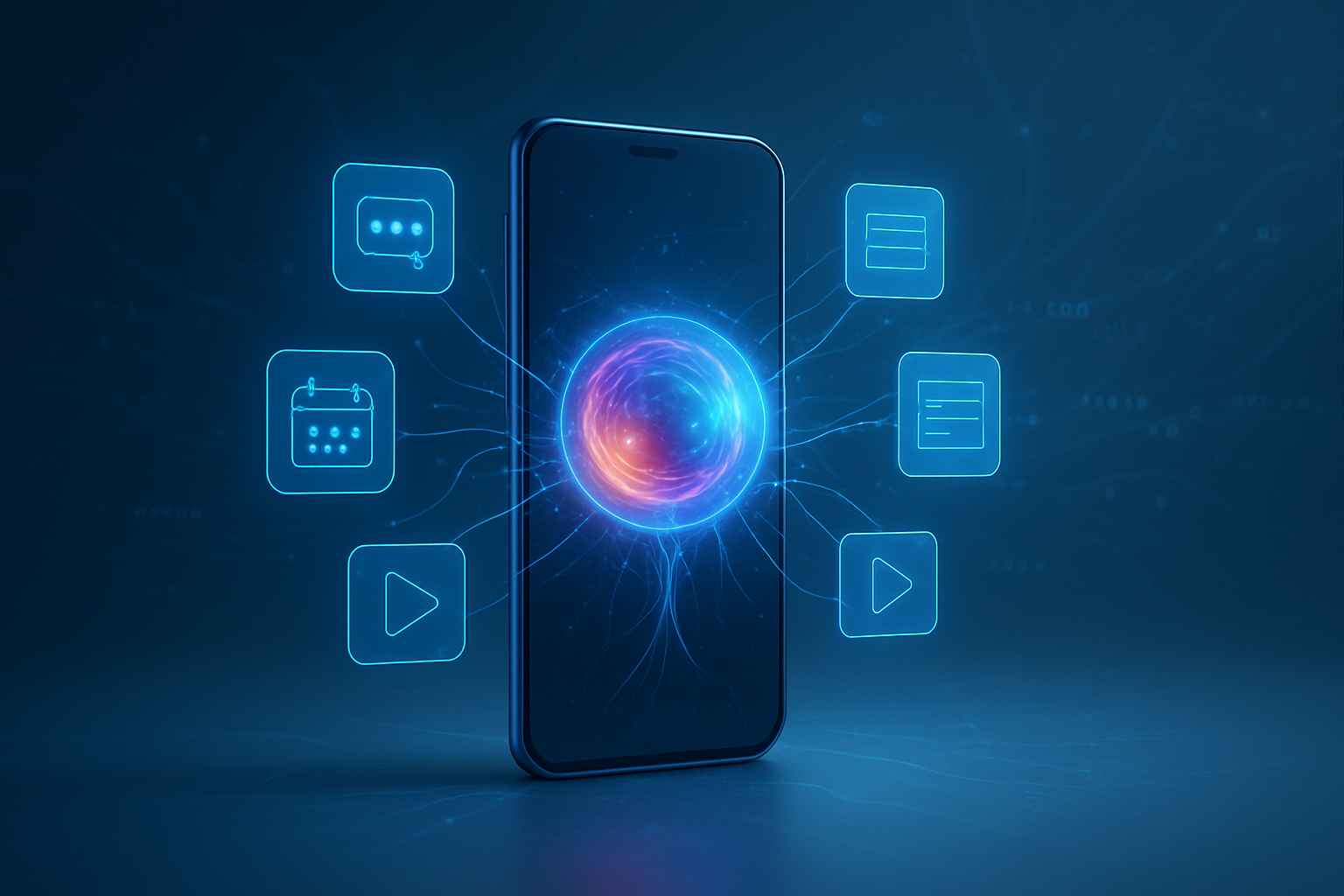
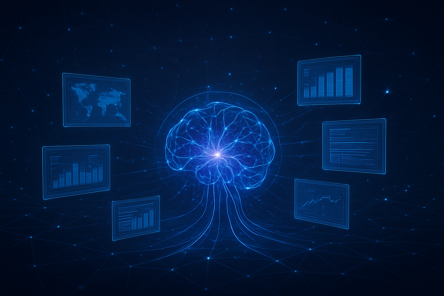
The immediate significance of Gemini Deep Research lies in its ability to navigate the open web with the precision of a human analyst. By browsing hundreds of disparate sources, cross-referencing data points, and identifying knowledge gaps in real-time, the agent can produce exhaustive, structured reports that were previously the domain of specialized research teams. As of late December 2025, this technology is already being integrated across the Google Workspace ecosystem, signaling a new era where "searching" for information is replaced by "delegating" complex objectives to an autonomous digital workforce.
The technical backbone of this advancement is Gemini 3 Pro, a model built on a sophisticated Sparse Mixture-of-Experts (MoE) architecture. While the model boasts a total parameter count exceeding 1 trillion, its efficiency is maintained by activating only 15 to 20 billion parameters per query, allowing for high-speed reasoning and lower latency. One of the most significant technical leaps is the introduction of a "Thinking" mode, which allows users to toggle between standard responses and extended internal reasoning. In "High" thinking mode, the model engages in deep chain-of-thought processing, making it ideal for the complex causal chains required for investigative research.
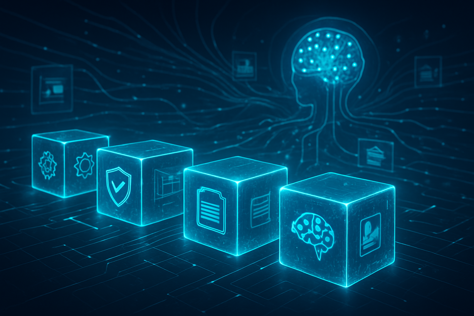
Gemini Deep Research differentiates itself from previous "browsing" features by its level of autonomy. Rather than just summarizing a few search results, the agent operates in a continuous loop: it creates a research plan, browses hundreds of sites, reads PDFs, analyzes data tables, and even accesses a user’s private Google Drive or Gmail if permitted. If it encounters conflicting information, it autonomously seeks out a third source to resolve the discrepancy. The final output is not a chat bubble, but a multi-page structured report exported to Google Canvas, PDF, or even an interactive "Audio Overview" that summarizes the findings in a podcast-like format.
Initial reactions from the AI research community have been focused on the new "DeepSearchQA" benchmark released alongside the tool. This benchmark, consisting of 900 complex "causal chain" tasks, suggests that Gemini 3 Pro is the first model to consistently solve research problems that require more than 20 independent steps of logic. Industry experts have noted that the model’s 10 million-token context window—specifically optimized for the "Code Assist" and "Research" variants—allows it to maintain perfect "needle-in-a-haystack" recall over massive datasets, a feat that previous generations of LLMs struggled to achieve consistently.
The release of Gemini Deep Research has sent shockwaves through the competitive landscape, placing immense pressure on rivals like OpenAI and Anthropic. Following the initial November launch of Gemini 3 Pro, reports surfaced that OpenAI—heavily backed by Microsoft (NASDAQ:MSFT)—declared an internal "Code Red," leading to the accelerated release of GPT-5.2. While OpenAI's models remain highly competitive in creative reasoning, Google’s deep integration with Chrome and Workspace gives Gemini a strategic advantage in "grounding" its research in real-world, real-time data that other labs struggle to access as seamlessly.
For startups and specialized research firms, the implications are disruptive. Services that previously charged thousands of dollars for market intelligence or due diligence reports are now facing a reality where a $20-a-month subscription can generate comparable results in minutes. This shift is likely to benefit enterprise-scale companies that can now deploy thousands of these agents to monitor global supply chains or legal filings. Meanwhile, Amazon (NASDAQ:AMZN)-backed Anthropic has responded with Claude Opus 4.5, positioning it as the "safer" and more "human-aligned" alternative for sensitive corporate research, though it currently lacks the sheer breadth of Google’s autonomous browsing capabilities.
Market analysts suggest that Google’s strategic positioning is now focused on "Duration of Autonomy"—a new metric measuring how long an agent can work without human correction. By winning the "agent wars" of 2025, Google has effectively pivoted from being a search engine company to an "action engine" company. This transition is expected to bolster Google’s cloud revenue as enterprises move their data into the Google Cloud (NASDAQ:GOOGL) environment to take full advantage of the Gemini 3 Pro reasoning core.
The broader significance of Gemini Deep Research lies in its potential to solve the "information overload" problem that has plagued the internet for decades. We are moving into a landscape where the primary value of AI is no longer its ability to write text, but its ability to filter and synthesize the vast, messy sea of human knowledge into actionable insights. However, this breakthrough is not without its concerns. The "death of search" as we know it could lead to a significant decline in traffic for independent publishers and journalists, as AI agents scrape content and present it in summarized reports, bypassing the original source's advertising or subscription models.
Furthermore, the rise of autonomous investigative agents raises critical questions about academic integrity and misinformation. If an agent can browse hundreds of sites to support a specific (and potentially biased) hypothesis, the risk of "automated confirmation bias" becomes a reality. Critics point out that while Gemini 3 Pro is highly capable, its ability to distinguish between high-quality evidence and sophisticated "AI-slop" on the web will be the ultimate test of its utility. This marks a milestone in AI history comparable to the release of the first web browser; it is not just a tool for viewing the internet, but a tool for reconstructing it.
Comparisons are already being drawn to the "AlphaGo moment" for general intelligence. While AlphaGo proved AI could master a closed system with fixed rules, Gemini Deep Research is proving that AI can master the open, chaotic system of human information. This transition from "Generative AI" to "Agentic AI" signifies the end of the first chapter of the LLM era and the beginning of a period where AI is defined by its agency and its ability to impact the physical and digital worlds through independent action.
Looking ahead, the next 12 to 18 months are expected to see the expansion of these agents into "multimodal action." While Gemini Deep Research currently focuses on information gathering and reporting, the next logical step is for the agent to execute tasks based on its findings—such as booking travel, filing legal paperwork, or even initiating software patches in response to a discovered security vulnerability. Experts predict that the "Thinking" parameters of Gemini 3 will continue to scale, eventually allowing for "overnight" research tasks that involve thousands of steps and complex simulations.
One of the primary challenges that remains is the cost of compute. While the MoE architecture makes Gemini 3 Pro efficient, running a "Deep Research" query that hits hundreds of sites is still significantly more expensive than a standard search. We can expect to see a tiered economy of agents, where "Flash" agents handle quick lookups and "Pro" agents are reserved for high-stakes strategic decisions. Additionally, the industry must address the "robot exclusion" protocols of the web; as more sites block AI crawlers, the "open" web that these agents rely on may begin to shrink, leading to a new era of gated data and private knowledge silos.
Google’s announcement of Gemini Deep Research and the Gemini 3 Pro model marks a watershed moment in the evolution of artificial intelligence. By successfully bridging the gap between a chatbot and a fully autonomous investigative agent, Google has redefined the boundaries of what a digital assistant can achieve. The ability to browse, synthesize, and report on hundreds of sources in a matter of minutes represents a massive leap in productivity for researchers, analysts, and students alike.
As we move into 2026, the key takeaway is that the "agentic era" has arrived. The significance of this development in AI history cannot be overstated; it is the moment AI moved from being a participant in human conversation to a partner in human labor. In the coming weeks and months, the tech world will be watching closely to see how OpenAI and Anthropic respond, and how the broader internet ecosystem adapts to a world where the most frequent "visitors" to a website are no longer humans, but autonomous agents searching for the truth.
This content is intended for informational purposes only and represents analysis of current AI developments.
TokenRing AI delivers enterprise-grade solutions for multi-agent AI workflow orchestration, AI-powered development tools, and seamless remote collaboration platforms.
For more information, visit https://www.tokenring.ai/.