Oracle (NYSE: ORCL) has fundamentally reshaped the landscape of the "Cloud Wars" by announcing a staggering $50 billion capital-raising plan for 2026, aimed squarely at funding the most ambitious AI data center expansion in history. This massive influx of capital—split between debt and equity—is designed to fuel the construction of "Giga-scale" data center campuses and the procurement of hundreds of thousands of high-performance GPUs, cementing Oracle’s position as the primary engine for the next generation of artificial intelligence.
The move marks a definitive pivot for the enterprise software giant, transforming it into a top-tier infrastructure provider capable of rivaling established hyperscalers like Amazon (NASDAQ: AMZN) and Microsoft (NASDAQ: MSFT). By securing this funding, Oracle is directly addressing an unprecedented $523 billion backlog in contracted demand, much of which is driven by its multi-year, multi-billion dollar agreements with frontier AI labs such as OpenAI and Elon Musk’s xAI.
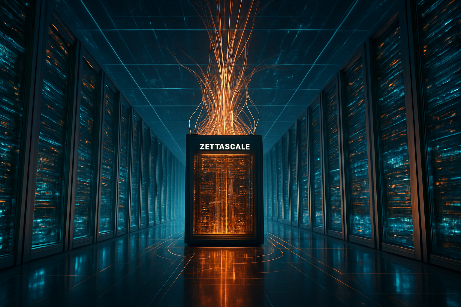
Technical Dominance: 800,000 GPUs and the Zettascale Frontier
At the heart of Oracle’s strategy is a technical partnership with NVIDIA (NASDAQ: NVDA) that pushes the boundaries of computational scale. Oracle is currently deploying the NVIDIA GB200 NVL72 Blackwell racks, which utilize advanced liquid-cooling systems to manage the intense thermal demands of frontier model training. While previous generations of clusters were measured in thousands of GPUs, Oracle is now moving toward "Zettascale" infrastructure.
The company’s crown jewel is the newly unveiled Zettascale10 cluster, slated for general availability in the second half of 2026. This system is engineered to interconnect up to 800,000 NVIDIA GPUs across a high-density campus within a strict 2km radius to maintain low-latency communication. According to technical specifications, the Zettascale10 is expected to deliver an astronomical 16 ZettaFLOPS of peak performance. This represents a monumental leap over current industry standards, where a cluster of 100,000 GPUs was considered the "state of the art" only a year ago.
To power these behemoths, Oracle is moving beyond traditional energy grids. The flagship "Stargate" site in Abilene, Texas, which is being developed in conjunction with OpenAI, features a modular power architecture designed to scale to 5 gigawatts (GW). Oracle has even secured permits for small modular nuclear reactors (SMRs) to ensure a dedicated, carbon-neutral, and stable energy source for these compute clusters. This shift to sovereign energy production highlights the extreme physical requirements of modern AI, differentiating Oracle’s infrastructure from standard cloud offerings that remain tethered to municipal utility constraints.
Market Positioning: The $523 Billion Backlog and the "Whale" Strategy
The financial implications of this expansion are underscored by Oracle’s record-breaking Remaining Performance Obligation (RPO). As of the end of 2025, Oracle reported a total backlog of $523 billion, a staggering 438% increase year-over-year. This backlog isn't just a theoretical number; it represents legally binding contracts from "whale" customers including Meta (NASDAQ: META), NVIDIA, and OpenAI. Oracle’s $300 billion, 5-year deal with OpenAI alone has positioned it as the primary infrastructure provider for the "Stargate" project, an initiative aimed at building the world’s most powerful AI supercomputer.
Industry analysts suggest that Oracle is successfully outmaneuvering its larger rivals by offering more flexible deployment models. While AWS and Azure have traditionally focused on standardized, massive-scale regions, Oracle’s "Dedicated Regions" allow companies and even entire nations to have their own private OCI cloud inside their own data centers. This has made Oracle the preferred choice for sovereign AI projects—nations that want to maintain data residency and control over their computational resources while still accessing cutting-edge Blackwell hardware.
Furthermore, Oracle’s strategy focuses on its existing dominance in enterprise data. Larry Ellison, Oracle’s co-founder and CTO, has emphasized that while the race to train public LLMs is intense, the ultimate "Holy Grail" is reasoning over private corporate data. Because the vast majority of the world's high-value business data already resides in Oracle databases, the company is uniquely positioned to offer an integrated stack where AI models can perform secure RAG (Retrieval-Augmented Generation) directly against a company's proprietary records without the data ever leaving the Oracle ecosystem.
Wider Significance: The Geopolitics of Compute and Energy
The scale of Oracle’s $50 billion raise reflects a broader trend in the AI landscape: the transition from "Big Tech" to "Big Infrastructure." We are witnessing a shift where the ability to build and power massive physical structures is becoming as important as the ability to write code. Oracle’s move into nuclear energy and Giga-scale campuses signals that the AI race is no longer just a software competition, but a race for physical resources—land, power, and silicon.
This development also raises significant questions about the concentration of power in the AI industry. With Oracle, Microsoft, and NVIDIA forming a tight-knit ecosystem of infrastructure and hardware, the barrier to entry for new competitors in the "frontier model" space has become virtually insurmountable. The capital requirements alone—now measured in tens of billions for a single year's buildout—suggest that only a handful of corporations and well-funded nation-states will be able to participate in the highest levels of AI development.
However, the rapid expansion is not without its risks. In early 2026, Oracle faced a class-action lawsuit from bondholders who alleged the company was not transparent enough about the debt leverage required for this aggressive buildout. This highlights a potential concern for the market: the "AI bubble" risk. If the revenue from these massive clusters does not materialize as quickly as the debt matures, even a giant like Oracle could face financial strain. Nonetheless, the current $523 billion RPO suggests that demand is currently far outstripping supply.
Future Developments: Toward 1 Million GPUs and Sovereign AI
Looking ahead, Oracle’s roadmap suggests that the Zettascale10 is only the beginning. Rumors of a "Mega-Cluster" featuring over 1 million GPUs by 2027 are already circulating in the research community. As NVIDIA continues to iterate on its Blackwell and future Rubin architectures, Oracle is expected to remain a "launch partner" for every new generation of silicon.
The near-term focus will be on the successful deployment of the Abilene site and the integration of SMR technology. If Oracle can prove that nuclear-powered data centers are a viable and scalable solution, it will likely prompt a massive wave of similar investments from competitors. Additionally, expect to see Oracle expand its "Sovereign Cloud" footprint into the Middle East and Southeast Asia, where nations are increasingly looking to develop their own "National AI" capabilities to avoid dependence on U.S. or Chinese public clouds.
The primary challenge remains the supply chain and power grid stability. While Oracle has the capital, the physical procurement of transformers, liquid-cooling components, and specialized construction labor remains a bottleneck for the entire industry. How quickly Oracle can convert its "dry powder" into operational racks will determine its success in the coming 24 months.
Conclusion: A New Era of Hyperscale Dominance
Oracle’s $50 billion funding raise and its massive pivot to AI infrastructure represent one of the most significant shifts in the company's 49-year history. By leveraging its existing enterprise data moat and forming deep, foundational partnerships with NVIDIA and OpenAI, Oracle has transformed from a "legacy" database firm into the most aggressive player in the AI hardware race.
The sheer scale of the Zettascale10 clusters and the $523 billion backlog indicate that the demand for AI compute is not just a passing trend but a fundamental restructuring of the global economy. Oracle’s willingness to bet the balance sheet on nuclear-powered data centers and nearly a million GPUs suggests that we are entering a "Giga-scale" era where the winners will be determined by who can build the most robust physical foundations for the digital minds of the future.
In the coming months, investors and tech observers should watch for the first operational milestones at the Abilene site and the formal launch of the 800,000 GPU cluster. These will be the true litmus tests for Oracle’s ambitious vision. If successful, Oracle will have secured its place as the backbone of the AI era for decades to come.
This content is intended for informational purposes only and represents analysis of current AI developments.
TokenRing AI delivers enterprise-grade solutions for multi-agent AI workflow orchestration, AI-powered development tools, and seamless remote collaboration platforms.
For more information, visit https://www.tokenring.ai/.