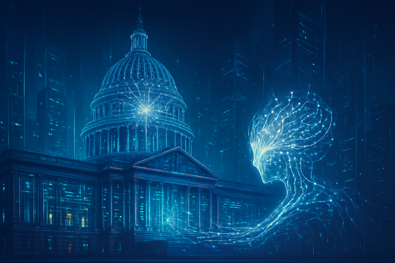
The relentless pursuit of artificial intelligence (AI) advancements is igniting an unprecedented demand for a new breed of digital infrastructure: specialized AI data centers. These facilities, purpose-built to handle the immense computational and energy requirements of modern AI workloads, are rapidly becoming the bedrock of the AI revolution. From training colossal language models to powering real-time analytics, traditional data centers are proving increasingly inadequate, paving the way for a global surge in investment and development. A prime example of this critical infrastructure shift is the proposed $300 million AI data center in Lewiston, Maine, a project emblematic of the industry's pivot towards dedicated AI compute power.
This monumental investment in Lewiston, set to redevelop the historic Bates Mill No. 3, underscores a broader trend where cities and regions are vying to become hubs for the next generation of industrial powerhouses – those fueled by artificial intelligence. The project, spearheaded by MillCompute, aims to transform the vacant mill into a Tier III AI data center, signifying a commitment to high availability and continuous operation crucial for demanding AI tasks. As AI continues to permeate every facet of technology and business, the race to build and operate these specialized computational fortresses is intensifying, signaling a fundamental reshaping of the digital landscape.
Engineering the Future: The Technical Demands of AI Data Centers
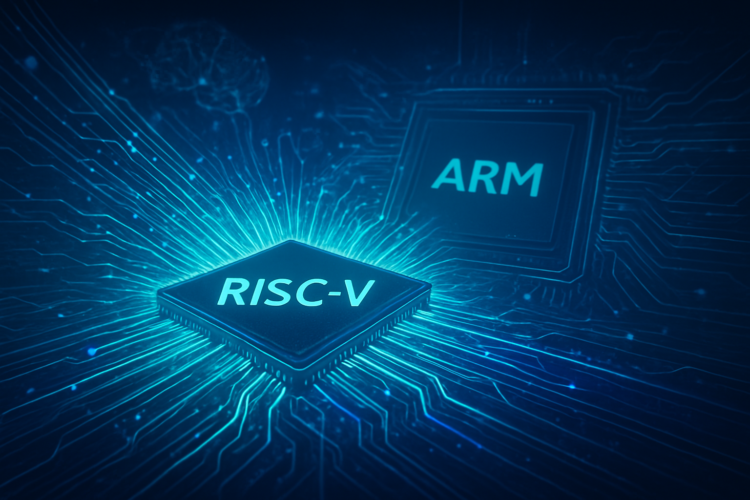
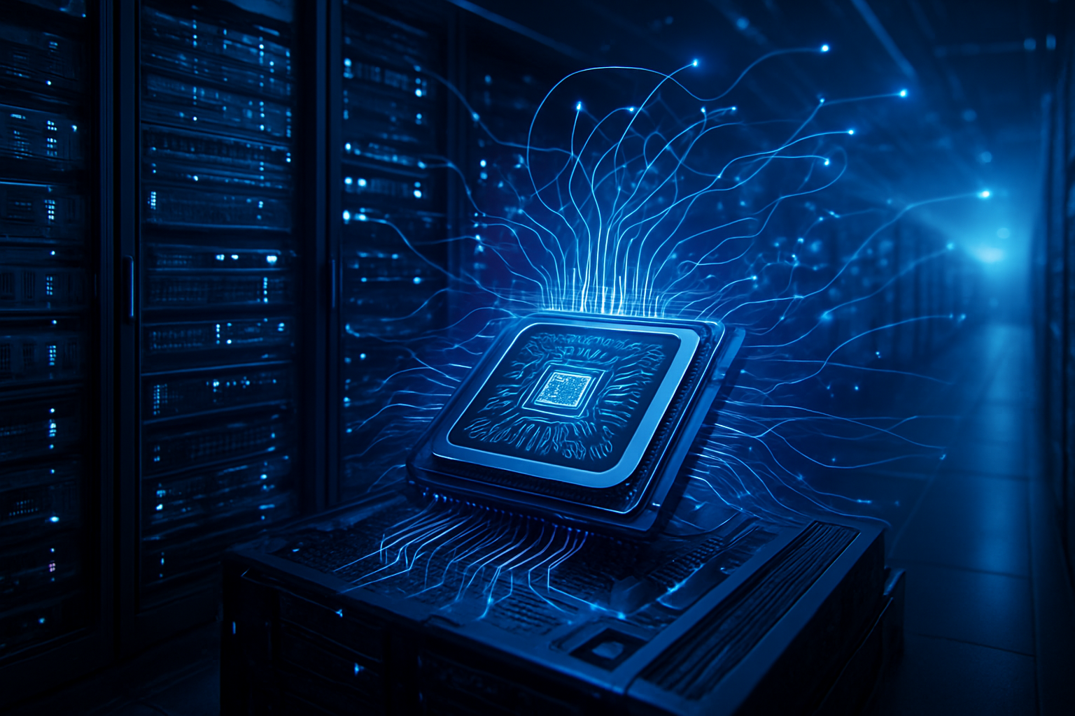
The technical specifications and capabilities of specialized AI data centers mark a significant departure from their conventional predecessors. The core difference lies in the sheer computational intensity and the unique hardware required for AI workloads, particularly for deep learning and machine learning model training. Unlike general-purpose servers, AI systems heavily rely on specialized accelerators such as Graphics Processing Units (GPUs) and Tensor Processing Units (TPUs), which are optimized for parallel processing and capable of performing millions of computations per second. This demand for powerful hardware is pushing rack densities from a typical 5-15kW to an astonishing 50-100kW+, with some cutting-edge designs even reaching 250kW per rack.
Such extreme power densities bring with them unprecedented challenges, primarily in energy consumption and thermal management. Traditional air-cooling systems, once the standard, are often insufficient to dissipate the immense heat generated by these high-performance components. Consequently, AI data centers are rapidly adopting advanced liquid cooling solutions, including direct-to-chip and immersion cooling, which can reduce energy requirements for cooling by up to 95% while simultaneously enhancing performance and extending hardware lifespan. Furthermore, the rapid exchange of vast datasets inherent in AI operations necessitates robust network infrastructure, featuring high-speed, low-latency, and high-bandwidth fiber optic connectivity to ensure seamless communication between thousands of processors.
The global AI data center market reflects this technical imperative, projected to explode from $236.44 billion in 2025 to $933.76 billion by 2030, at a compound annual growth rate (CAGR) of 31.6%. This exponential growth highlights how current infrastructure is simply not designed to efficiently handle the petabytes of data and complex algorithms that define modern AI. The shift is not merely an upgrade but a fundamental redesign, prioritizing power availability, advanced cooling, and optimized network architectures to unlock the full potential of AI.
Reshaping the AI Ecosystem: Impact on Companies and Competitive Dynamics
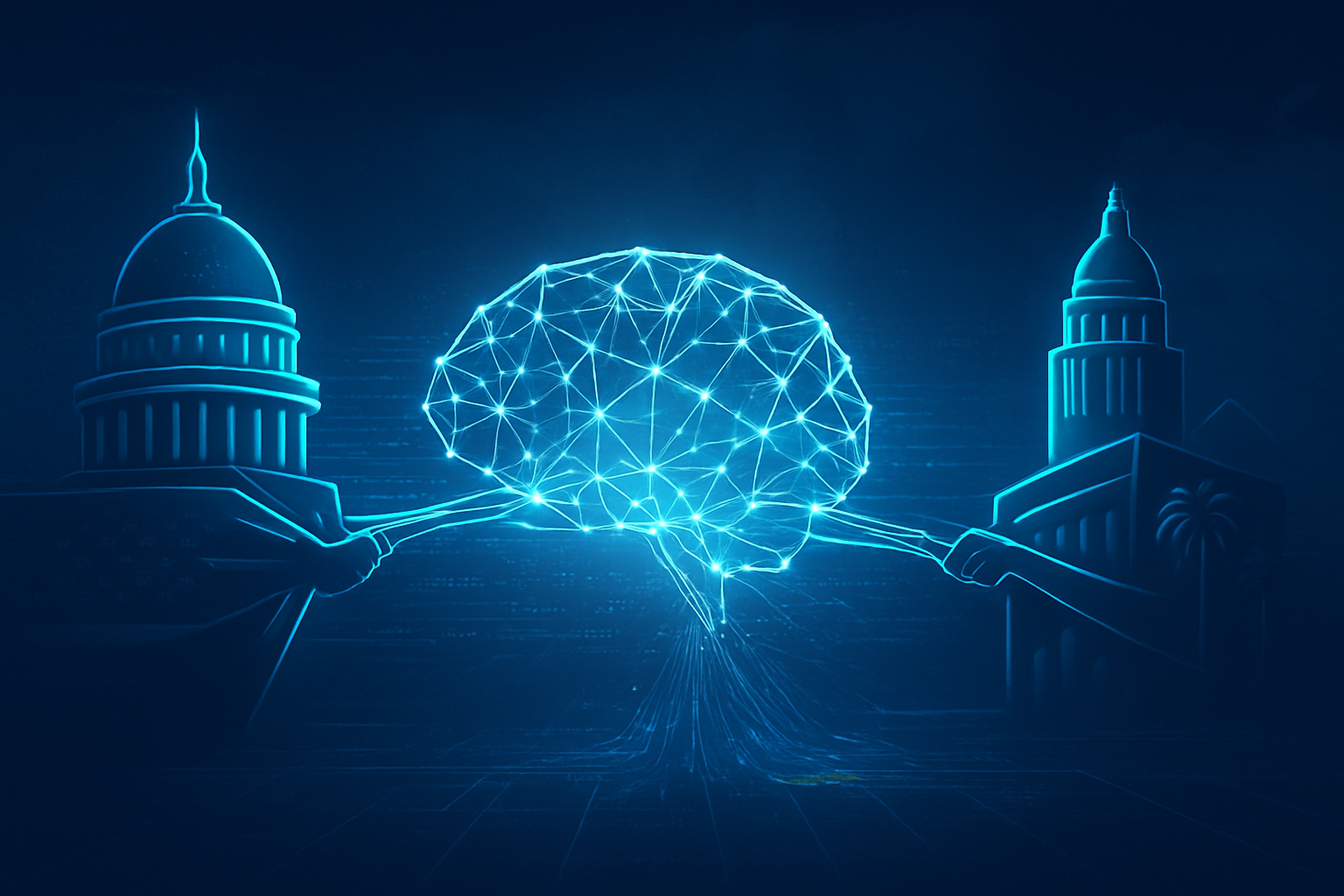
The proliferation of specialized AI data centers has profound implications for AI companies, tech giants, and startups alike, fundamentally reshaping the competitive landscape. Hyperscalers and cloud computing providers, such as Amazon (NASDAQ: AMZN), Microsoft (NASDAQ: MSFT), Google (NASDAQ: GOOGL), and Meta (NASDAQ: META), are at the forefront of this investment wave, pouring billions into building next-generation AI-optimized infrastructure. These companies stand to benefit immensely by offering scalable, high-performance AI compute resources to a vast customer base, cementing their market positioning as essential enablers of AI innovation.
For major AI labs and tech companies, access to these specialized data centers is not merely an advantage but a necessity for staying competitive. The ability to quickly train larger, more complex models, conduct extensive research, and deploy sophisticated AI services hinges on having robust, dedicated infrastructure. Companies without direct access or significant investment in such facilities may find themselves at a disadvantage in the race to develop and deploy cutting-edge AI. This development could lead to a further consolidation of power among those with the capital and foresight to invest heavily in AI infrastructure, potentially creating barriers to entry for smaller startups.
However, specialized AI data centers also create new opportunities. Companies like MillCompute, focusing on developing and operating these facilities, are emerging as critical players in the AI supply chain. Furthermore, the demand for specialized hardware, advanced cooling systems, and energy solutions fuels innovation and growth for manufacturers and service providers in these niche areas. The market is witnessing a strategic realignment where the physical infrastructure supporting AI is becoming as critical as the algorithms themselves, driving new partnerships, acquisitions, and a renewed focus on strategic geographical placement for optimal power and cooling.
The Broader AI Landscape: Impacts, Concerns, and Milestones
The increasing demand for specialized AI data centers fits squarely into the broader AI landscape as a critical trend shaping the future of technology. It underscores that the AI revolution is not just about algorithms and software, but equally about the underlying physical infrastructure that makes it possible. This infrastructure boom is driving a projected 165% increase in global data center power demand by 2030, primarily fueled by AI workloads, necessitating a complete rethinking of how digital infrastructure is designed, powered, and operated.
The impacts are wide-ranging, from economic development in regions hosting these facilities, like Lewiston, to significant environmental concerns. The immense energy consumption of AI data centers raises questions about sustainability and carbon footprint. This has spurred a strong push towards renewable energy integration, including on-site generation, battery storage, and hybrid power systems, as companies strive to meet corporate sustainability commitments and mitigate environmental impact. Site selection is increasingly prioritizing energy availability and access to green power sources over traditional factors.
This era of AI infrastructure build-out can be compared to previous technological milestones, such as the dot-com boom that drove the construction of early internet data centers or the expansion of cloud infrastructure in the 2010s. However, the current scale and intensity of demand, driven by the unique computational requirements of AI, are arguably unprecedented. Potential concerns beyond energy consumption include the concentration of AI power in the hands of a few major players, the security of these critical facilities, and the ethical implications of the AI systems they support. Nevertheless, the investment in specialized AI data centers is a clear signal that the world is gearing up for a future where AI is not just an application, but the very fabric of our digital existence.
The Road Ahead: Future Developments and Expert Predictions
Looking ahead, the trajectory of specialized AI data centers points towards several key developments. Near-term, we can expect a continued acceleration in the adoption of advanced liquid cooling technologies, moving from niche solutions to industry standards as rack densities continue to climb. There will also be an increased focus on AI-optimized facility design, with data centers being built from the ground up to accommodate high-performance GPUs, NVMe SSDs for ultra-fast storage, and high-speed networking like InfiniBand. Experts predict that the global data center infrastructure market, fueled by the AI arms race, will surpass $1 trillion in annual spending by 2030.
Long-term, the integration of edge computing with AI is poised to gain significant traction. As AI applications demand lower latency and real-time processing, compute resources will increasingly be pushed closer to end-users and data sources. This will likely lead to the development of smaller, distributed AI-specific data centers at the edge, complementing the hyperscale facilities. Furthermore, research into more energy-efficient AI hardware and algorithms will become paramount, alongside innovations in heat reuse technologies, where waste heat from data centers could be repurposed for district heating or other industrial processes.
Challenges that need to be addressed include securing reliable and abundant clean energy sources, managing the complex supply chains for specialized hardware, and developing skilled workforces to operate and maintain these advanced facilities. Experts predict a continued strategic global land grab for sites with robust power grids, access to renewable energy, and favorable climates for natural cooling. The evolution of specialized AI data centers will not only shape the capabilities of AI itself but also influence energy policy, urban planning, and environmental sustainability for decades to come.
A New Foundation for the AI Age
The emergence and rapid expansion of specialized data centers to support AI computations represent a pivotal moment in the history of artificial intelligence. Projects like the $300 million AI data center in Lewiston are not merely construction endeavors; they are the foundational keystones for the next era of technological advancement. The key takeaway is clear: the future of AI is inextricably linked to the development of purpose-built, highly efficient, and incredibly powerful infrastructure designed to meet its unique demands.
This development signifies AI's transition from a nascent technology to a mature, infrastructure-intensive industry. Its significance in AI history is comparable to the invention of the microchip or the widespread adoption of the internet, as it provides the essential physical layer upon which all future AI breakthroughs will be built. The long-term impact will be a world increasingly powered by intelligent systems, with access to unprecedented computational power enabling solutions to some of humanity's most complex challenges.
In the coming weeks and months, watch for continued announcements of new AI data center projects, further advancements in cooling and power management technologies, and intensified competition among cloud providers to offer the most robust AI compute services. The race to build the ultimate AI infrastructure is on, and its outcome will define the capabilities and trajectory of artificial intelligence for generations.
This content is intended for informational purposes only and represents analysis of current AI developments.
TokenRing AI delivers enterprise-grade solutions for multi-agent AI workflow orchestration, AI-powered development tools, and seamless remote collaboration platforms.
For more information, visit https://www.tokenring.ai/.