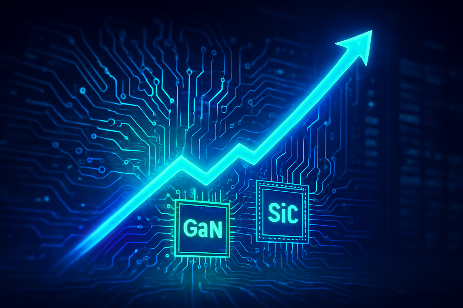
Category: Uncategorized

  • Opera Unleashes Agentic AI Browser, Neon, with a Bold $19.90 Monthly Subscription

    Opera Unleashes Agentic AI Browser, Neon, with a Bold $19.90 Monthly Subscription

    In a significant move that could redefine the landscape of web browsing, Opera (NASDAQ: OPRA) has officially launched its groundbreaking new AI-powered browser, Opera Neon, on September 30, 2025. This premium offering, distinct from its existing free AI assistant Aria, is positioned as an "agentic AI browser" designed to proactively assist users with complex tasks, moving beyond mere conversational AI to an era where the browser acts on behalf of the user. The most striking aspect of this launch is its subscription model, priced at $19.90 per month, a strategic decision that immediately places it in direct competition with leading standalone AI services.

    The introduction of Opera Neon marks a pivotal moment for the browser market, traditionally dominated by free offerings. Opera's gamble on a premium, subscription-based AI browser signals a belief that a segment of users, particularly power users and professionals, will be willing to pay for advanced, proactive AI capabilities integrated deeply into their browsing experience. This bold pricing strategy will undoubtedly spark debate and force a re-evaluation of how AI value is delivered and monetized within the tech industry.

    Diving Deep into Opera Neon's Agentic AI Engine

    Opera Neon is not just another browser with an AI chatbot; it represents a fundamental shift towards an "agentic" web experience. At its core, Neon is engineered to be a proactive partner, capable of organizing and completing tasks autonomously. Unlike basic AI assistants that respond to prompts, Neon's "agentic AI capabilities," dubbed Neon Do, allow the browser to perform actions such as filling out forms, comparing data across multiple sites, or even drafting code directly within the browser environment. It can intelligently open and close tabs and execute actions within them using its integrated AI, offering a level of automation previously unseen in mainstream browsers.

    A key differentiator for Neon is its concept of Tasks. These are self-contained AI workspaces that inherently understand context, enabling the AI to analyze, compare, and act across various sources simultaneously without interfering with other open tabs. Imagine Neon creating a "mini-browser" for each task, allowing the AI to assist within that specific context—for instance, researching a product by pulling specifications from multiple sites, comparing prices, and even booking a demo, all within one cohesive task environment. Furthermore, Cards provide a new interface with reusable prompt templates, allowing users to automate repetitive workflows. These cards can be mixed and matched like a deck of AI behaviors, or users can leverage community-shared templates, streamlining complex interactions.

    Opera emphasizes Neon's privacy-first design, with all sensitive AI actions and data processing occurring locally on the device. This local execution model gives users greater control over their data, ensuring that login credentials and payment details remain private, a significant appeal for those concerned about data privacy in an AI-driven world. Beyond its agentic features, Neon also empowers users with direct code generation and the ability to build mini-applications within the browser. This comprehensive suite of features contrasts sharply with previous approaches, which primarily offered sidebar chatbots or basic content summarization. While Opera's free AI assistant, Aria (available since May 2023 and powered by OpenAI's GPT models and Google's Gemini models), offers multifunctional chat, summarization, translation, image generation, and coding support, Neon elevates the experience to autonomous task execution. Initial reactions from the AI research community and industry experts highlight the ambitious nature of Neon Do, recognizing it as a significant step towards truly intelligent, proactive agents within the everyday browsing interface.

    Market Shake-Up: Implications for AI Companies and Tech Giants

    Opera Neon's premium pricing strategy has immediate and profound implications for both established tech giants and agile AI startups. Companies like Microsoft (NASDAQ: MSFT) with Copilot, Google (NASDAQ: GOOGL) with Gemini, and OpenAI with ChatGPT Plus, all of whom offer similarly priced premium AI subscriptions (typically around $20/month), now face a direct competitor in a new form factor: the browser itself. Opera's move validates the idea of a premium tier for advanced AI functionalities, potentially encouraging other browser developers to explore similar models beyond basic, free AI integrations.

    The competitive landscape is poised for disruption. While Microsoft's Copilot is deeply integrated into Windows and Edge, and Google's Gemini into its vast ecosystem, Opera Neon carves out a niche by focusing on browser-centric "agentic AI." This could challenge the current market positioning where AI is often a feature within an application or operating system, rather than the primary driver of the application itself. Companies that can effectively demonstrate a superior, indispensable value proposition in agentic AI features, particularly those that go beyond conversational AI to truly automate tasks, stand to benefit.

    However, the $19.90 price tag presents a significant hurdle. Users will scrutinize whether Opera Neon's specialized features offer enough of a productivity boost to justify a cost comparable to or higher than comprehensive AI suites like ChatGPT Plus, Microsoft Copilot Pro, or Google Gemini Advanced. These established services often provide broader AI capabilities across various platforms and applications, not just within a browser. Startups in the AI browser space, such as Perplexity's Comet (which is currently free), will need to carefully consider their own monetization strategies in light of Opera's bold move. The potential disruption to existing products lies in whether users will see the browser as the ultimate hub for AI-driven productivity, pulling them away from standalone AI tools or AI features embedded in other applications.

    Wider Significance: A New Frontier in AI-Human Interaction

    Opera Neon's launch fits squarely into the broader AI landscape's trend towards more sophisticated, proactive, and embedded AI. It represents a significant step beyond the initial wave of generative AI chatbots, pushing the boundaries towards truly "agentic" AI that can understand intent and execute multi-step tasks. This development underscores the growing demand for AI that can not only generate content or answer questions but also actively assist in workflows, thereby augmenting human productivity.

    The impact could be transformative for how we interact with the web. Instead of manually navigating, copying, and pasting information, an agentic browser could handle these mundane tasks, freeing up human cognitive load for higher-level decision-making. Potential concerns, however, revolve around user trust and control. While Opera emphasizes local execution for privacy, the idea of an AI agent autonomously performing actions raises questions about potential misinterpretations, unintended consequences, or the feeling of relinquishing too much control to an algorithm. Comparisons to previous AI milestones, such as the advent of search engines or the first personal digital assistants, highlight Neon's potential to fundamentally alter web interaction, moving from passive consumption to active, AI-orchestrated engagement.

    This move also signals a maturing AI market where companies are exploring diverse monetization strategies. The browser market, traditionally a battleground of free offerings, is now seeing a premium tier emerge, driven by advanced AI. This could lead to a bifurcation of the browser market: free, feature-rich browsers with basic AI, and premium, subscription-based browsers offering deep, agentic AI capabilities.

    The Road Ahead: Future Developments and Challenges

    Looking ahead, the success of Opera Neon will likely catalyze further innovation in the AI browser space. We can expect near-term developments to focus on refining Neon's agentic capabilities, expanding its "Tasks" and "Cards" ecosystems, and improving its local execution models for even greater privacy and efficiency. Opera's commitment to rolling out upgraded AI tools, including faster models and higher usage limits, to its free browser portfolio (Opera One, Opera GX, Opera Air) suggests a two-pronged strategy: mass adoption of basic AI, and premium access to advanced agency.

    Potential applications and use cases on the horizon for agentic browsers are vast. Imagine an AI browser that can autonomously manage your travel bookings, research and compile comprehensive reports from disparate sources, or even proactively identify and resolve technical issues on websites you frequent. For developers, the ability to generate code and build mini-applications directly within the browser could accelerate prototyping and deployment.

    However, significant challenges need to be addressed. Overcoming user skepticism about paying for a browser, especially when many competitors offer robust AI features for free, will be crucial. The perceived value of "agentic AI" must be demonstrably superior and indispensable for users to justify the monthly cost. Furthermore, ensuring the reliability, accuracy, and ethical deployment of autonomous AI agents within a browser will be an ongoing technical and societal challenge. Experts predict that if Opera Neon gains traction, it could accelerate the development of more sophisticated agentic AI across the tech industry, prompting other major players to invest heavily in similar browser-level AI integrations.

    A New Chapter in AI-Driven Browsing

    Opera Neon's launch with a $19.90 monthly subscription marks a bold and potentially transformative moment in the evolution of AI and web browsing. The key takeaway is Opera's commitment to "agentic AI," moving beyond conversational assistants to a browser that proactively executes tasks on behalf of the user. This strategy represents a significant bet on the willingness of power users to pay a premium for enhanced productivity and automation, challenging the long-standing paradigm of free browser software.

    The significance of this development in AI history lies in its potential to usher in a new era of human-computer interaction, where the browser becomes less of a tool and more of an intelligent partner. It forces a re-evaluation of the value proposition of AI, pushing the boundaries of what users expect from their daily digital interfaces. While the $19.90 price point will undoubtedly be a major talking point and a barrier for some, its success or failure will offer invaluable insights into the future of AI monetization and user adoption. In the coming weeks and months, the tech world will be closely watching user reception, competitive responses, and the practical demonstrations of Neon's agentic capabilities to determine if Opera has truly opened a new chapter in AI-driven browsing.

    This content is intended for informational purposes only and represents analysis of current AI developments.

    TokenRing AI delivers enterprise-grade solutions for multi-agent AI workflow orchestration, AI-powered development tools, and seamless remote collaboration platforms.
    For more information, visit https://www.tokenring.ai/.

  • Advanced Packaging: The Unsung Hero Powering the Next-Generation AI Revolution

    Advanced Packaging: The Unsung Hero Powering the Next-Generation AI Revolution

    As Artificial Intelligence (AI) continues its relentless march into every facet of technology, the demands placed on underlying hardware have escalated to unprecedented levels. Traditional chip design, once the sole driver of performance gains through transistor miniaturization, is now confronting its physical and economic limits. In this new era, an often- overlooked yet critically important field – advanced packaging technologies – has emerged as the linchpin for unlocking the true potential of next-generation AI chips, fundamentally reshaping how we design, build, and optimize computing systems for the future. These innovations are moving far beyond simply protecting a chip; they are intricate architectural feats that dramatically enhance power efficiency, performance, and cost-effectiveness.

    This paradigm shift is driven by the insatiable appetite of modern AI workloads, particularly large generative language models, for immense computational power, vast memory bandwidth, and high-speed interconnects. Advanced packaging technologies provide a crucial "More than Moore" pathway, allowing the industry to continue scaling performance even as traditional silicon scaling slows. By enabling the seamless integration of diverse, specialized components into a single, optimized package, advanced packaging is not just an incremental improvement; it is a foundational transformation that directly addresses the "memory wall" bottleneck and fuels the rapid advancement of AI capabilities across various sectors.

    The Technical Marvels Underpinning AI's Leap Forward

    The core of this revolution lies in several sophisticated packaging techniques that enable a new level of integration and performance. These technologies depart significantly from conventional 2D packaging, which typically places individual chips on a planar Printed Circuit Board (PCB), leading to longer signal paths and higher latency.

    2.5D Packaging, exemplified by Taiwan Semiconductor Manufacturing Company (TSMC) (NYSE: TSM)'s CoWoS (Chip-on-Wafer-on-Substrate) and Intel (NASDAQ: INTC)'s Embedded Multi-die Interconnect Bridge (EMIB), involves placing multiple active dies—such as a powerful GPU and High-Bandwidth Memory (HBM) stacks—side-by-side on a high-density silicon or organic interposer. This interposer acts as a miniature, high-speed wiring board, drastically shortening interconnect distances from centimeters to millimeters. This reduction in path length significantly boosts signal integrity, lowers latency, and reduces power consumption for inter-chip communication. NVIDIA (NASDAQ: NVDA)'s H100 and A100 series GPUs, along with Advanced Micro Devices (AMD) (NASDAQ: AMD)'s Instinct MI300A accelerators, are prominent examples leveraging 2.5D integration for unparalleled AI performance.

    3D Packaging, or 3D-IC, takes vertical integration to the next level by stacking multiple active semiconductor dies directly on top of each other. These layers are interconnected through Through-Silicon Vias (TSVs), tiny electrical conduits etched directly through the silicon. This vertical stacking minimizes footprint, maximizes integration density, and offers the shortest possible interconnects, leading to superior speed and power efficiency. Samsung (KRX: 005930)'s X-Cube and Intel's Foveros are leading 3D packaging technologies, with AMD utilizing TSMC's 3D SoIC (System-on-Integrated-Chips) for its Ryzen 7000X3D CPUs and EPYC processors.

    A cutting-edge advancement, Hybrid Bonding, forms direct, molecular-level connections between metal pads of two or more dies or wafers, eliminating the need for traditional solder bumps. This technology is critical for achieving interconnect pitches below 10 µm, with copper-to-copper (Cu-Cu) hybrid bonding reaching single-digit micrometer ranges. Hybrid bonding offers vastly higher interconnect density, shorter wiring distances, and superior electrical performance, leading to thinner, faster, and more efficient chips. NVIDIA's Hopper and Blackwell series AI GPUs, along with upcoming Apple (NASDAQ: AAPL) M5 series AI chips, are expected to heavily rely on hybrid bonding.

    Finally, Fan-Out Wafer-Level Packaging (FOWLP) is a cost-effective, high-performance solution. Here, individual dies are repositioned on a carrier wafer or panel, with space around each die for "fan-out." A Redistribution Layer (RDL) is then formed over the entire molded area, creating fine metal traces that "fan out" from the chip's original I/O pads to a larger array of external contacts. This approach allows for a higher I/O count, better signal integrity, and a thinner package compared to traditional fan-in packaging. TSMC's InFO (Integrated Fan-Out) technology, famously used in Apple's A-series processors, is a prime example, and NVIDIA is reportedly considering Fan-Out Panel Level Packaging (FOPLP) for its GB200 AI server chips due to CoWoS capacity constraints.

    The initial reaction from the AI research community and industry experts has been overwhelmingly positive. Advanced packaging is widely recognized as essential for extending performance scaling beyond traditional transistor miniaturization, addressing the "memory wall" by dramatically increasing bandwidth, and enabling new, highly optimized heterogeneous computing architectures crucial for modern AI. The market for advanced packaging, especially for high-end 2.5D/3D approaches, is projected to experience significant growth, reaching tens of billions of dollars by the end of the decade.

    Reshaping the AI Industry: A New Competitive Landscape

    The advent and rapid evolution of advanced packaging technologies are fundamentally reshaping the competitive dynamics within the AI industry, creating new opportunities and strategic imperatives for tech giants and startups alike.

    Companies that stand to benefit most are those heavily invested in custom AI hardware and high-performance computing. Tech giants like Google (NASDAQ: GOOGL), Amazon (NASDAQ: AMZN), and Microsoft (NASDAQ: MSFT) are leveraging advanced packaging for their custom AI chips (such as Google's Tensor Processing Units or TPUs and Microsoft's Azure Maia 100) to optimize hardware and software for their specific cloud-based AI workloads. This vertical integration provides them with significant strategic advantages in performance, latency, and energy efficiency. NVIDIA and AMD, as leading providers of AI accelerators, are at the forefront of adopting and driving these technologies, with NVIDIA's CEO Jensen Huang emphasizing advanced packaging as critical for maintaining a competitive edge.

    The competitive implications for major AI labs and tech companies are profound. TSMC (NYSE: TSM) has solidified its dominant position in advanced packaging with technologies like CoWoS and SoIC, rapidly expanding capacity to meet escalating global demand for AI chips. This positions TSMC as a "System Fab," offering comprehensive AI chip manufacturing services and enabling collaborations with innovative AI companies. Intel (NASDAQ: INTC), through its IDM 2.0 strategy and advanced packaging solutions like Foveros and EMIB, is also aggressively pursuing leadership in this space, offering these services to external customers via Intel Foundry Services (IFS). Samsung (KRX: 005930) is restructuring its chip packaging processes, aiming for a "one-stop shop" approach for AI chip production, integrating memory, foundry, and advanced packaging to reduce production time and offering differentiated capabilities, as evidenced by its strategic partnership with OpenAI.

    This shift also brings potential disruption to existing products and services. The industry is moving away from monolithic chip designs towards modular chiplet architectures, fundamentally altering the semiconductor value chain. The focus is shifting from solely front-end manufacturing to elevating the role of system design and emphasizing back-end design and packaging as critical drivers of performance and differentiation. This enables the creation of new, more capable AI-driven applications across industries, while also necessitating a re-evaluation of business models across the entire chipmaking ecosystem. For smaller AI startups, chiplet technology, facilitated by advanced packaging, lowers the barrier to entry by allowing them to leverage pre-designed components, reducing R&D time and costs, and fostering greater innovation in specialized AI hardware.

    A New Era for AI: Broader Significance and Strategic Imperatives

    Advanced packaging technologies represent a strategic pivot in the AI landscape, extending beyond mere hardware improvements to address fundamental challenges and enable the next wave of AI innovation. This development fits squarely within broader AI trends, particularly the escalating computational demands of large language models and generative AI. As traditional Moore's Law scaling encounters its limits, advanced packaging provides the crucial pathway for continued performance gains, effectively extending the lifespan of exponential progress in computing power for AI.

    The impacts are far-reaching: unparalleled performance enhancements, significant power efficiency gains (with chiplet-based designs offering 30-40% lower energy consumption for the same workload), and ultimately, cost advantages through improved manufacturing yields and optimized process node utilization. Furthermore, advanced packaging enables greater miniaturization, critical for edge AI and autonomous systems, and accelerates time-to-market for new AI hardware. It also enhances thermal management, a vital consideration for high-performance AI processors that generate substantial heat.

    However, this transformative shift is not without its concerns. The manufacturing complexity and associated costs of advanced packaging remain significant hurdles, potentially leading to higher production expenses and challenges in yield management. The energy-intensive nature of these processes also raises environmental impact concerns. Additionally, for AI to further optimize packaging processes, there's a pressing need for more robust data sharing and standardization across the industry, as proprietary information often limits collaborative advancements.

    Comparing this to previous AI milestones, advanced packaging represents a hardware-centric breakthrough that directly addresses the physical limitations encountered by earlier algorithmic advancements (like neural networks and deep learning) and traditional transistor scaling. It's a paradigm shift that moves away from monolithic chip designs towards modular chiplet architectures, offering a level of flexibility and customization at the hardware layer akin to the flexibility offered by software frameworks in early AI. This strategic importance cannot be overstated; it has become a competitive differentiator, democratizing AI hardware development by lowering barriers for startups, and providing the scalability and adaptability necessary for future AI systems.

    The Horizon: Glass, Light, and Unprecedented Integration

    The future of advanced packaging for AI chips promises even more revolutionary developments, pushing the boundaries of integration, performance, and efficiency.

    In the near term (next 1-3 years), we can expect intensified adoption of High-Bandwidth Memory (HBM), particularly HBM4, with increased capacity and speed to support ever-larger AI models. Hybrid bonding will become a cornerstone for high-density integration, and heterogeneous integration with chiplets will continue to dominate, allowing for modular and optimized AI accelerators. Emerging technologies like backside power delivery will also gain traction, improving power efficiency and signal integrity.

    Looking further ahead (beyond 3 years), truly transformative changes are on the horizon. Co-Packaged Optics (CPO), which integrates optical I/O directly with AI accelerators, is poised to replace traditional copper interconnects. This will drastically reduce power consumption and latency in multi-rack AI clusters and data centers, enabling faster and more efficient communication crucial for massive data movement.

    Perhaps one of the most significant long-term developments is the emergence of Glass-Core Substrates. These are expected to become a new standard, offering superior electrical, thermal, and mechanical properties compared to organic substrates. Glass provides ultra-low warpage, superior signal integrity, better thermal expansion matching with silicon, and enables higher-density packaging (supporting sub-2-micron vias). Intel projects complete glass substrate solutions in the second half of this decade, with companies like Samsung, Corning, and TSMC actively investing in this technology. While challenges exist, such as the brittleness of glass and manufacturing costs, its advantages for AI, HPC, and 5G are undeniable.

    Panel-Level Packaging (PLP) is also gaining momentum as a cost-effective alternative to wafer-level packaging, utilizing larger panel substrates to increase throughput and reduce manufacturing costs for high-performance AI packages.

    Experts predict a dynamic period of innovation, with the advanced packaging market projected to grow significantly, reaching approximately $80 billion by 2030. The package itself will become a crucial point of innovation and a differentiation driver for system performance, with value creation migrating towards companies that can design and integrate complex, system-level chip solutions. The accelerated adoption of hybrid bonding, TSVs, and advanced interposers is expected, particularly for high-end AI accelerators and data center CPUs. Major investments from key players like TSMC, Samsung, and Intel underscore the strategic importance of these technologies, with Intel's roadmap for glass substrates pushing Moore's Law beyond 2030. The integration of AI into electronic design automation (EDA) processes will further accelerate multi-die innovations, making chiplets a commercial reality.

    A New Foundation for AI's Future

    In conclusion, advanced packaging technologies are no longer merely a back-end manufacturing step; they are a critical front-end innovation driver, fundamentally powering the AI revolution. The convergence of 2.5D/3D integration, HBM, heterogeneous integration, the nascent promise of Co-Packaged Optics, and the revolutionary potential of glass-core substrates are unlocking unprecedented levels of performance and efficiency. These advancements are essential for the continued development of more sophisticated AI models, the widespread integration of AI across industries, and the realization of truly intelligent and autonomous systems.

    As we move forward, the semiconductor industry will continue its relentless pursuit of innovation in packaging, driven by the insatiable demands of AI. Key areas to watch in the coming weeks and months include further announcements from leading foundries on capacity expansion for advanced packaging, new partnerships between AI hardware developers and packaging specialists, and the first commercial deployments of emerging technologies like glass-core substrates and CPO in high-performance AI systems. The future of AI is intrinsically linked to the ingenuity and advancements in how we package our chips, making this field a central pillar of technological progress.

    This content is intended for informational purposes only and represents analysis of current AI developments.

    TokenRing AI delivers enterprise-grade solutions for multi-agent AI workflow orchestration, AI-powered development tools, and seamless remote collaboration platforms. For more information, visit https://www.tokenring.ai/.

  • AI’s Insatiable Hunger Drives Semiconductor Consolidation Frenzy

    AI’s Insatiable Hunger Drives Semiconductor Consolidation Frenzy

    The global semiconductor industry is in the throes of an unprecedented consolidation wave, fueled by the explosive demand for Artificial Intelligence (AI) and high-performance computing (HPC) chips. As of late 2025, a series of strategic mergers and acquisitions are fundamentally reshaping the market, with chipmakers aggressively pursuing specialized technologies and integrated solutions to power the next generation of AI innovation. This M&A supercycle reflects a critical pivot point for the tech industry, where the ability to design, manufacture, and integrate advanced silicon is paramount for AI leadership. Companies are no longer just seeking scale; they are strategically acquiring capabilities that enable "full-stack" AI solutions, from chip design and manufacturing to software and system integration, all to meet the escalating computational demands of modern AI models.

    Strategic Realignment in the Silicon Ecosystem

    The past two to three years have witnessed a flurry of high-stakes deals illustrating a profound shift in business strategy within the semiconductor sector. One of the most significant was AMD's (NASDAQ: AMD) acquisition of Xilinx in 2022 for $49 billion, which propelled AMD into a leadership position in adaptive computing. Integrating Xilinx's Field-Programmable Gate Arrays (FPGAs) and adaptive SoCs significantly bolstered AMD's offerings for data centers, automotive, and telecommunications, providing flexible, high-performance computing solutions critical for evolving AI workloads. More recently, in March 2025, AMD further solidified its data center AI accelerator market position by acquiring ZT Systems for $4.9 billion, integrating expertise in building and scaling large-scale computing infrastructure for hyperscale companies.

    Another notable move came from Broadcom (NASDAQ: AVGO), which acquired VMware in 2023 for $61 billion. While VMware is primarily a software company, this acquisition by a leading semiconductor firm underscores a broader trend of hardware-software convergence. Broadcom's foray into cloud computing and data center software reflects the increasing necessity for chipmakers to offer integrated solutions, extending their influence beyond traditional hardware components. Similarly, Synopsys's (NASDAQ: SNPS) monumental $35 billion acquisition of Ansys in January 2024 aimed to merge Ansys's advanced simulation and analysis capabilities with Synopsys's chip design software, a crucial step for optimizing the performance and efficiency of complex AI chips. In February 2025, NXP Semiconductors (NASDAQ: NXPI) acquired Kinara.ai for $307 million, gaining access to deep-tech AI processors to expand its global footprint and enhance its AI capabilities.

    These strategic maneuvers are driven by several core imperatives. The insatiable demand for AI and HPC requires highly specialized semiconductors capable of handling massive, parallel computations. Companies are acquiring niche firms to gain access to cutting-edge technologies like FPGAs, dedicated AI processors, advanced simulation software, and energy-efficient power management solutions. This trend towards "full-stack" solutions and vertical integration allows chipmakers to offer comprehensive, optimized platforms that combine hardware, software, and AI development capabilities, enhancing efficiency and performance from design to deployment. Furthermore, the escalating energy demands of AI workloads are making energy efficiency a paramount concern, prompting investments in or acquisitions of technologies that promote sustainable and efficient processing.

    Reshaping the AI Competitive Landscape

    This wave of semiconductor consolidation has profound implications for AI companies, tech giants, and startups alike. Companies like AMD and Nvidia (NASDAQ: NVDA), through strategic acquisitions and organic growth, are aggressively expanding their ecosystems to offer end-to-end AI solutions. AMD's integration of Xilinx and ZT Systems, for instance, positions it as a formidable competitor to Nvidia's established dominance in the AI accelerator market, especially in data centers and hyperscale environments. This intensified rivalry is fostering accelerated innovation, particularly in specialized AI chips, advanced packaging technologies like HBM (High Bandwidth Memory), and novel memory solutions crucial for the immense demands of large language models (LLMs) and complex AI workloads.

    Tech giants, often both consumers and developers of AI, stand to benefit from the enhanced capabilities and more integrated solutions offered by consolidated semiconductor players. However, they also face potential disruptions in their supply chains or a reduction in supplier diversity. Startups, particularly those focused on niche AI hardware or software, may find themselves attractive acquisition targets for larger entities seeking to quickly gain specific technological expertise or market share. Conversely, the increasing market power of a few consolidated giants could make it harder for smaller players to compete, potentially stifling innovation if not managed carefully. The shift towards integrated hardware-software platforms means that companies offering holistic AI solutions will gain significant strategic advantages, influencing market positioning and potentially disrupting existing products or services that rely on fragmented component sourcing.

    Broader Implications for the AI Ecosystem

    The consolidation within the semiconductor industry fits squarely into the broader AI landscape as a critical enabler and accelerant. It reflects the understanding that advanced AI is fundamentally bottlenecked by underlying silicon capabilities. By consolidating, companies aim to overcome these bottlenecks, accelerate the development of next-generation AI, and secure crucial supply chains amidst geopolitical tensions. This trend is reminiscent of past industry milestones, such as the rise of integrated circuit manufacturing or the PC revolution, where foundational hardware shifts enabled entirely new technological paradigms.

    However, this consolidation also raises potential concerns. Increased market dominance by a few large players could lead to reduced competition, potentially impacting pricing, innovation pace, and the availability of diverse chip architectures. Regulatory bodies worldwide are already scrutinizing these large-scale mergers, particularly regarding potential monopolies and cross-border technology transfers, which can delay or even block significant transactions. The immense power requirements of AI, coupled with the drive for energy-efficient chips, also highlight a growing challenge for sustainability. While consolidation can lead to more optimized designs, the overall energy footprint of AI continues to expand, necessitating significant investments in energy infrastructure and continued focus on green computing.

    The Road Ahead: Future Developments and Challenges

    Looking ahead, the semiconductor industry is poised for continued strategic M&A activity, driven by the relentless advancement of AI. Experts predict a continued focus on acquiring companies with expertise in specialized AI accelerators, neuromorphic computing, quantum computing components, and advanced packaging technologies that enable higher performance and lower power consumption. We can expect to see more fully integrated AI platforms emerging, offering turnkey solutions for various applications, from edge AI devices to hyperscale cloud infrastructure.

    Potential applications on the horizon include highly optimized chips for personalized AI, autonomous systems that can perform complex reasoning on-device, and next-generation data centers capable of supporting exascale AI training. Challenges remain, including the staggering costs of R&D, the increasing complexity of chip design, and the ongoing need to navigate geopolitical uncertainties that affect global supply chains. What experts predict will happen next is a continued convergence of hardware and software, with AI becoming increasingly embedded at every layer of the computing stack, demanding even more sophisticated and integrated silicon solutions.

    A New Era for AI-Powered Silicon

    In summary, the current wave of mergers, acquisitions, and consolidation in the semiconductor industry represents a pivotal moment in AI history. It underscores the critical role of specialized, high-performance silicon in unlocking the full potential of artificial intelligence. Key takeaways include the aggressive pursuit of "full-stack" AI solutions, the intensified rivalry among tech giants, and the strategic importance of energy efficiency in chip design. This consolidation is not merely about market share; it's about acquiring the fundamental building blocks for an AI-driven future.

    As we move into the coming weeks and months, it will be crucial to watch how these newly formed entities integrate their technologies, whether regulatory bodies intensify their scrutiny, and how the innovation fostered by this consolidation translates into tangible breakthroughs for AI applications. The long-term impact will likely be a more vertically integrated and specialized semiconductor industry, better equipped to meet the ever-growing demands of AI, but also one that requires careful attention to competition and ethical development.

    This content is intended for informational purposes only and represents analysis of current AI developments.

    TokenRing AI delivers enterprise-grade solutions for multi-agent AI workflow orchestration, AI-powered development tools, and seamless remote collaboration platforms. For more information, visit https://www.tokenring.ai/.

  • The Dawn of Decentralized Intelligence: Edge AI and Distributed Computing Reshape the Future

    The Dawn of Decentralized Intelligence: Edge AI and Distributed Computing Reshape the Future

    The world of Artificial Intelligence is experiencing a profound shift as specialized Edge AI processors and the trend towards distributed AI computing gain unprecedented momentum. This pivotal evolution is moving AI processing capabilities closer to the source of data, fundamentally transforming how intelligent systems operate across industries. This decentralization promises to unlock real-time decision-making, enhance data privacy, optimize bandwidth, and usher in a new era of pervasive and autonomous AI.

    This development signifies a departure from the traditional cloud-centric AI model, where data is invariably sent to distant data centers for processing. Instead, Edge AI empowers devices ranging from smartphones and industrial sensors to autonomous vehicles to perform complex AI tasks locally. Concurrently, distributed AI computing paradigms are enabling AI workloads to be spread across vast networks of interconnected systems, fostering scalability, resilience, and collaborative intelligence. The immediate significance lies in addressing critical limitations of centralized AI, paving the way for more responsive, secure, and efficient AI applications that are deeply integrated into our physical world.

    Technical Deep Dive: The Silicon and Software Powering the Edge Revolution

    The core of this transformation lies in the sophisticated hardware and innovative software architectures enabling AI at the edge and across distributed networks. Edge AI processors are purpose-built for efficient AI inference, optimized for low power consumption, compact form factors, and accelerated neural network computation.

    Key hardware advancements include:

    • Neural Processing Units (NPUs): Dedicated accelerators like Google's (NASDAQ: GOOGL) Edge TPU ASICs (e.g., in the Coral Dev Board) deliver high INT8 performance (e.g., 4 TOPS at ~2 Watts), enabling real-time execution of models like MobileNet V2 at hundreds of frames per second.
    • Specialized GPUs: NVIDIA's (NASDAQ: NVDA) Jetson series (e.g., Jetson AGX Orin with up to 275 TOPS, Jetson Orin Nano with up to 40 TOPS) integrates powerful GPUs with Tensor Cores, offering configurable power envelopes and supporting complex models for vision and natural language processing.
    • Custom ASICs: Companies like Qualcomm (NASDAQ: QCOM) (Snapdragon-based platforms with Hexagon Tensor Accelerators, e.g., 15 TOPS on RB5 platform), Rockchip (RK3588 with 6 TOPS NPU), and emerging players like Hailo (Hailo-10 for GenAI at 40 TOPS INT4) and Axelera AI (Metis chip with 214 TOPS peak performance) are designing chips specifically for edge AI, offering unparalleled efficiency.

    These specialized processors differ significantly from previous approaches by enabling on-device processing, drastically reducing latency by eliminating cloud roundtrips, enhancing data privacy by keeping sensitive information local, and conserving bandwidth. Unlike cloud AI, which leverages massive data centers, Edge AI demands highly optimized models (quantization, pruning) to fit within the limited resources of edge hardware.

    Distributed AI computing, on the other hand, focuses on spreading computational tasks across multiple nodes. Federated Learning (FL) stands out as a privacy-preserving technique where a global AI model is trained collaboratively on decentralized data from numerous edge devices. Only model updates (weights, gradients) are exchanged, never the raw data. For large-scale model training, parallelism is crucial: Data Parallelism replicates models across devices, each processing different data subsets, while Model Parallelism (tensor or pipeline parallelism) splits the model itself across multiple GPUs for extremely large architectures.

    The AI research community and industry experts have largely welcomed these advancements. They highlight the immense benefits in privacy, real-time capabilities, bandwidth/cost efficiency, and scalability. However, concerns remain regarding the technical complexity of managing distributed frameworks, data heterogeneity in FL, potential security vulnerabilities (e.g., inference attacks), and the resource constraints of edge devices, which necessitate continuous innovation in model optimization and deployment strategies.

    Industry Impact: A Shifting Competitive Landscape

    The advent of Edge AI and distributed AI is fundamentally reshaping the competitive dynamics for tech giants, AI companies, and startups alike, creating new opportunities and potential disruptions.

    Tech Giants like Microsoft (NASDAQ: MSFT) (Azure IoT Edge), Google (NASDAQ: GOOGL) (Edge TPU, Google Cloud), Amazon (NASDAQ: AMZN) (AWS IoT Greengrass), and IBM (NYSE: IBM) are heavily investing, extending their comprehensive cloud and AI services to the edge. Their strategic advantage lies in vast R&D resources, existing cloud infrastructure, and extensive customer bases, allowing them to offer unified platforms for seamless edge-to-cloud AI deployment. Many are also developing custom silicon (ASICs) to optimize performance and reduce reliance on external suppliers, intensifying hardware competition.

    Chipmakers and Hardware Providers are primary beneficiaries. NVIDIA (NASDAQ: NVDA), Intel (NASDAQ: INTC) (Core Ultra processors), Qualcomm (NASDAQ: QCOM), and AMD (NASDAQ: AMD) are at the forefront, developing the specialized, energy-efficient processors and memory solutions crucial for edge devices. Companies like TSMC (NYSE: TSM) also benefit from increased demand for advanced chip manufacturing. Altera (NASDAQ: ALTR) (an Intel (NASDAQ: INTC) company) is also seeing FPGAs emerge as compelling alternatives for specific, optimized edge AI inference.

    Startups are finding fertile ground in niche areas, developing innovative edge AI chips (e.g., Hailo, Axelera AI) and offering specialized platforms and tools that democratize edge AI development (e.g., Edge Impulse). They can compete by delivering best-in-class solutions for specific problems, leveraging diverse hardware and cloud offerings to reduce vendor dependence.

    The competitive implications include a shift towards "full-stack" AI solutions where companies offering both software/models and underlying hardware/infrastructure gain significant advantages. There's increased competition in hardware, with hyperscalers developing custom ASICs challenging traditional GPU dominance. The democratization of AI development through user-friendly platforms will lower barriers to entry, while a trend towards consolidation around major generative AI platforms will also occur. Edge AI's emphasis on data sovereignty and security creates a competitive edge for providers prioritizing local processing and compliance.

    Potential disruptions include reduced reliance on constant cloud connectivity for certain AI services, impacting cloud providers if they don't adapt. Traditional data center energy and cooling solutions face disruption due to the extreme power density of AI hardware. Legacy enterprise software could be disrupted by agentic AI, capable of autonomous workflows at the edge. Services hampered by latency or bandwidth (e.g., autonomous vehicles) will see existing cloud-dependent solutions replaced by superior edge AI alternatives.

    Strategic advantages for companies will stem from offering real-time intelligence, robust data privacy, bandwidth optimization, and hybrid AI architectures that seamlessly distribute workloads between cloud and edge. Building strong ecosystem partnerships and focusing on industry-specific customizations will also be critical.

    Wider Significance: A New Era of Ubiquitous Intelligence

    Edge AI and distributed AI represent a profound milestone in the broader AI landscape, signifying a maturation of AI deployment that moves beyond purely algorithmic breakthroughs to focus on where and how intelligence operates.

    This fits into the broader AI trend of the cloud continuum, where AI workloads dynamically shift between centralized cloud and decentralized edge environments. The proliferation of IoT devices and the demand for instantaneous, private processing have necessitated this shift. The rise of micro AI, lightweight models optimized for resource-constrained devices, is a direct consequence.

    The overall impacts are transformative: drastically reduced latency enabling real-time decision-making in critical applications, enhanced data security and privacy by keeping sensitive information localized, and lower bandwidth usage and operational costs. Edge AI also fosters increased efficiency and autonomy, allowing devices to function independently even with intermittent connectivity, and contributes to sustainability by reducing the energy footprint of massive data centers. New application areas are emerging in computer vision, digital twins, and conversational agents.

    However, significant concerns accompany this shift. Resource limitations on edge devices necessitate highly optimized models. Model consistency and management across vast, distributed networks introduce complexity. While enhancing privacy, the distributed nature broadens the attack surface, demanding robust security measures. Management and orchestration complexity for geographically dispersed deployments, along with heterogeneity and fragmentation in the edge ecosystem, remain key challenges.

    Compared to previous AI milestones – from early AI's theoretical foundations and expert systems to the deep learning revolution of the 2010s – this era is distinguished by its focus on hardware infrastructure and the ubiquitous deployment of AI. While past breakthroughs focused on what AI could do, Edge and Distributed AI emphasize where and how AI can operate efficiently and securely, overcoming the practical limitations of purely centralized approaches. It's about integrating AI deeply into our physical world, making it pervasive and responsive.

    Future Developments: The Road Ahead for Decentralized AI

    The trajectory for Edge AI processors and distributed AI computing points towards a future of even greater autonomy, efficiency, and intelligence embedded throughout our environment.

    In the near-term (1-3 years), we can expect:

    • More Powerful and Efficient AI Accelerators: The market for AI-specific chips is projected to soar, with more advanced TPUs, GPUs, and custom ASICs (like NVIDIA's (NASDAQ: NVDA) GB10 Grace-Blackwell SiP and RTX 50-series) becoming standard, capable of running sophisticated models with less power.
    • Neuromorphic Processing Units (NPUs) in Consumer Devices: NPUs are becoming commonplace in smartphones and laptops, enabling real-time, low-latency AI at the edge.
    • Agentic AI: The emergence of "agentic AI" will see edge devices, models, and frameworks collaborating to make autonomous decisions and take actions without constant human intervention.
    • Accelerated Shift to Edge Inference: The focus will intensify on deploying AI models closer to data sources to deliver real-time insights, with the AI inference market projected for substantial growth.
    • 5G Integration: The global rollout of 5G will provide the ultra-low latency and high-bandwidth connectivity essential for large-scale, real-time distributed AI.

    Long-term (5+ years), more fundamental shifts are anticipated:

    • Neuromorphic Computing: Brain-inspired architectures, integrating memory and processing, will offer significant energy efficiency and continuous learning capabilities at the edge.
    • Optical/Photonic AI Chips: Research-grade optical AI chips, utilizing light for operations, promise substantial efficiency gains.
    • Truly Decentralized AI: The future may involve harnessing the combined power of billions of personal and corporate devices globally, offering exponentially greater compute power than centralized data centers, enhancing privacy and resilience.
    • Multi-Agent Systems and Swarm Intelligence: Multiple AI agents will learn, collaborate, and interact dynamically, leading to complex collective behaviors.
    • Blockchain Integration: Distributed inferencing could combine with blockchain for enhanced security and trust, verifying outputs across networks.
    • Sovereign AI: Driven by data sovereignty needs, organizations and governments will increasingly deploy AI at the edge to control data flow.

    Potential applications span autonomous systems (vehicles, drones, robots), smart cities (traffic management, public safety), healthcare (real-time diagnostics, wearable monitoring), Industrial IoT (quality control, predictive maintenance), and smart retail.

    However, challenges remain: technical limitations of edge devices (power, memory), model optimization and performance consistency across diverse environments, scalability and management complexity of vast distributed infrastructures, interoperability across fragmented ecosystems, and robust security and privacy against new attack vectors. Experts predict significant market growth for edge AI, with 50% of enterprises adopting edge computing by 2029 and 75% of enterprise-managed data processed outside traditional data centers by 2025. The rise of agentic AI and hardware innovation are seen as critical for the next decade of AI.

    Comprehensive Wrap-up: A Transformative Shift Towards Pervasive AI

    The rise of Edge AI processors and distributed AI computing marks a pivotal, transformative moment in the history of Artificial Intelligence. This dual-pronged revolution is fundamentally decentralizing intelligence, moving AI capabilities from monolithic cloud data centers to the myriad devices and interconnected systems at the very edge of our networks.

    The key takeaways are clear: decentralization is paramount, enabling real-time intelligence crucial for critical applications. Hardware innovation, particularly specialized AI processors, is the bedrock of this shift, facilitating powerful computation within constrained environments. Edge AI and distributed AI are synergistic, with the former handling immediate local inference and the latter enabling scalable training and broader application deployment. Crucially, this shift directly addresses mounting concerns regarding data privacy, security, and the sheer volume of data generated by an relentlessly connected world.

    This development's significance in AI history cannot be overstated. It represents a maturation of AI, moving beyond the foundational algorithmic breakthroughs of machine learning and deep learning to focus on the practical, efficient, and secure deployment of intelligence. It is about making AI pervasive, deeply integrated into our physical world, and responsive to immediate needs, overcoming the inherent latency, bandwidth, and privacy limitations of a purely centralized model. This is as impactful as the advent of cloud computing itself, democratizing access to AI and empowering localized, autonomous intelligence on an unprecedented scale.

    The long-term impact will be profound. We anticipate a future characterized by pervasive autonomy, where countless devices make sophisticated, real-time decisions independently, creating hyper-responsive and intelligent environments. This will lead to hyper-personalization while maintaining user privacy, and reshape industries from manufacturing to healthcare. Furthermore, the inherent energy efficiency of localized processing will contribute to a more sustainable AI ecosystem, and the democratization of AI compute may foster new economic models. However, vigilance regarding ethical and societal considerations will be paramount as AI becomes more distributed and autonomous.

    In the coming weeks and months, watch for continued processor innovation – more powerful and efficient TPUs, GPUs, and custom ASICs. The accelerating 5G rollout will further bolster Edge AI capabilities. Significant advancements in software and orchestration tools will be crucial for managing complex, distributed deployments. Expect further developments and wider adoption of federated learning for privacy-preserving AI. The integration of Edge AI with emerging generative and agentic AI will unlock new possibilities, such as real-time data synthesis and autonomous decision-making. Finally, keep an eye on how the industry addresses persistent challenges such as resource limitations, interoperability, and robust edge security. The journey towards truly ubiquitous and intelligent AI is just beginning.

    This content is intended for informational purposes only and represents analysis of current AI developments.

    TokenRing AI delivers enterprise-grade solutions for multi-agent AI workflow orchestration, AI-powered development tools, and seamless remote collaboration platforms.
    For more information, visit https://www.tokenring.ai/.

  • AI’s Insatiable Appetite: Memory Chips Enter a Decade-Long Supercycle

    AI’s Insatiable Appetite: Memory Chips Enter a Decade-Long Supercycle

    The artificial intelligence (AI) industry, as of October 2025, is driving an unprecedented surge in demand for memory chips, fundamentally reshaping the markets for DRAM (Dynamic Random-Access Memory) and NAND Flash. This insatiable appetite for high-performance and high-capacity memory, fueled by the exponential growth of generative AI, machine learning, and advanced analytics, has ignited a "supercycle" in the memory sector, leading to significant price hikes, looming supply shortages, and a strategic pivot in manufacturing focus. Memory is no longer a mere component but a strategic bottleneck and a critical enabler for the continued advancement and deployment of AI, with some experts predicting this demand-driven market could persist for a decade.

    The immediate significance for the AI industry is profound. High-Bandwidth Memory (HBM), a specialized type of DRAM, is at the epicenter of this transformation, experiencing explosive growth rates. Its superior speed, efficiency, and lower power consumption are indispensable for AI training and high-performance computing (HPC) platforms. Simultaneously, NAND Flash, particularly in high-capacity enterprise Solid State Drives (SSDs), is becoming crucial for storing the massive datasets that feed these AI models. This dynamic environment necessitates strategic procurement and investment in advanced memory solutions for AI developers and infrastructure providers globally.

    The Technical Evolution: HBM, LPDDR6, 3D DRAM, and CXL Drive AI Forward

    The technical evolution of DRAM and NAND Flash memory is rapidly accelerating to overcome the "memory wall"—the performance gap between processors and traditional memory—which is a major bottleneck for AI workloads. Innovations are focused on higher bandwidth, greater capacity, and improved power efficiency, transforming memory into a central pillar of AI hardware design.

    High-Bandwidth Memory (HBM) remains critical, with HBM3 and HBM3E as current standards and HBM4 anticipated by late 2025. HBM4 is projected to achieve speeds of 10+ Gbps, double the channel count per stack, and offer a significant 40% improvement in power efficiency over HBM3. Its stacked architecture, utilizing Through-Silicon Vias (TSVs) and advanced packaging, is indispensable for AI accelerators like those from NVIDIA (NASDAQ: NVDA) and AMD (NASDAQ: AMD), which require rapid transfer of large data volumes for training large language models (LLMs). Beyond HBM, the concept of 3D DRAM is evolving to integrate processing capabilities directly within the memory. Startups like NEO Semiconductor are developing "3D X-AI" technology, proposing 3D-stacked DRAM with integrated neuron circuitry that could boost AI performance by up to 100 times and increase memory density by 8 times compared to current HBM, while dramatically cutting power consumption by 99%.

    For power-efficient AI, particularly at the edge, the newly published JEDEC LPDDR6 standard is a game-changer. Elevating per-bit speed to 14.4 Gbps and expanding the data width, LPDDR6 delivers a total bandwidth of 691 Gb/s—twice that of LPDDR5X. This makes it ideal for AI inference models and edge workloads that require reduced latency and improved throughput with irregular, high-frequency access patterns. Cadence Design Systems (NASDAQ: CDNS) has already announced LPDDR6/5X memory IP achieving these breakthrough speeds. Meanwhile, Compute Express Link (CXL) is emerging as a transformative interface standard. CXL allows systems to expand memory capacity, pool and share memory dynamically across CPUs, GPUs, and accelerators, and ensures cache coherency, significantly improving memory utilization and efficiency for AI. Wolley Inc., for example, introduced a CXL memory expansion controller at FMS2025 that provides both memory and storage interfaces simultaneously over shared PCIe ports, boosting bandwidth and reducing total cost of ownership for running LLM inference.

    In the realm of storage, NAND Flash memory is also undergoing significant advancements. Manufacturers continue to scale 3D NAND with more layers, with Samsung (KRX: 005930) beginning mass production of its 9th-generation QLC V-NAND. Quad-Level Cell (QLC) NAND, with its higher storage density and lower cost, is increasingly adopted in enterprise SSDs for AI inference, where read operations dominate. SK Hynix (KRX: 000660) has announced mass production of the world's first 321-layer 2Tb QLC NAND flash, scheduled to enter the AI data center market in the first half of 2026. Furthermore, SanDisk (NASDAQ: SNDK) and SK Hynix are collaborating to co-develop High Bandwidth Flash (HBF), which integrates HBM-like concepts with NAND-based technology, aiming to provide a denser memory tier with 8-16 times more memory in the same footprint as HBM, with initial samples expected in late 2026. Industry experts widely acknowledge these advancements as critical for overcoming the "memory wall" and enabling the next generation of powerful, energy-efficient AI hardware, despite significant challenges related to power consumption and infrastructure costs.

    Reshaping the AI Industry: Beneficiaries, Battles, and Breakthroughs

    The dynamic trends in DRAM and NAND Flash memory are fundamentally reshaping the competitive landscape for AI companies, tech giants, and startups, creating significant beneficiaries, intensifying competitive battles, and driving strategic shifts. The overarching theme is that memory is no longer a commodity but a strategic asset, dictating the performance and efficiency of AI systems.

    Memory providers like SK Hynix (KRX: 000660), Samsung (KRX: 005930), and Micron Technology (NASDAQ: MU) are the primary beneficiaries of this AI-driven memory boom. Their strategic shift towards HBM production, significant R&D investments in HBM4, 3D DRAM, and LPDDR6, and advanced packaging techniques are crucial for maintaining leadership. SK Hynix, in particular, has emerged as a dominant force in HBM, with Micron's HBM capacity for 2025 and much of 2026 already sold out. These companies have become crucial partners in the AI hardware supply chain, gaining increased influence on product development, pricing, and competitive positioning. Hyperscalers such as Google (NASDAQ: GOOGL), Microsoft (NASDAQ: MSFT), Meta Platforms (NASDAQ: META), and Amazon (NASDAQ: AMZN), who are at the forefront of AI infrastructure build-outs, are driving massive demand for advanced memory. They are strategically investing in developing their own custom silicon, like Google's TPUs and Amazon's Trainium, to optimize performance and integrate memory solutions tightly with their AI software stacks, actively deploying CXL for memory pooling and exploring QLC NAND for cost-effective, high-capacity data storage.

    The competitive implications are profound. AI chip designers like NVIDIA (NASDAQ: NVDA), AMD (NASDAQ: AMD), and Intel (NASDAQ: INTC) are heavily reliant on advanced HBM for their AI accelerators. Their ability to deliver high-performance chips with integrated or tightly coupled advanced memory is a key competitive differentiator. NVIDIA's upcoming Blackwell GPUs, for instance, will heavily leverage HBM4. The emergence of CXL is enabling a shift towards memory-centric and composable architectures, allowing for greater flexibility, scalability, and cost efficiency in AI data centers, disrupting traditional server designs and favoring vendors who can offer CXL-enabled solutions like GIGABYTE Technology (TPE: 2376). For AI startups, while the demand for specialized AI chips and novel architectures presents opportunities, access to cutting-edge memory technologies like HBM can be a challenge due to high demand and pre-orders by larger players. Managing the increasing cost of advanced memory and storage is also a crucial factor for their financial viability and scalability, making strategic partnerships with memory providers or cloud giants offering advanced memory infrastructure critical for success.

    The potential for disruption is significant. The proposed mass production of 3D DRAM with integrated AI processing, offering immense density and performance gains, could fundamentally redefine the memory landscape, potentially displacing HBM as the leading high-performance memory solution for AI in the longer term. Similarly, QLC NAND's cost-effectiveness for large datasets, coupled with its performance suitability for read-heavy AI inference, positions it as a disruptive force against traditional HDDs and even some TLC-based SSDs in AI storage. Strategic partnerships, such as OpenAI's collaborations with Samsung and SK Hynix for its "Stargate" project, are becoming crucial for securing supply and co-developing next-generation memory solutions tailored for specific AI workloads.

    Wider Significance: Powering the AI Revolution with Caution

    The advancements in DRAM and NAND Flash memory technologies are fundamentally reshaping the broader Artificial Intelligence (AI) landscape, enabling more powerful, efficient, and sophisticated AI systems across various applications, from large-scale data centers to pervasive edge devices. These innovations are critical in overcoming the "memory wall" and fueling the AI revolution, but they also introduce new concerns and significant societal impacts.

    The ability of HBM to feed data to powerful AI accelerators, LPDDR6's role in enabling efficient edge AI, 3D DRAM's potential for in-memory processing, and CXL's capacity for memory pooling are all crucial for the next generation of AI. QLC NAND's cost-effectiveness for storing massive AI datasets complements these high-performance memory solutions. This fits into the broader AI landscape by providing the foundational hardware necessary for scaling large language models, enabling real-time AI inference, and expanding AI capabilities to power-constrained environments. The increased memory bandwidth and capacity are directly enabling the development of more complex and context-aware AI systems.

    However, these advancements also bring forth a range of potential concerns. As AI systems gain "near-infinite memory" and can retain detailed information about user interactions, concerns about data privacy intensify. If AI is trained on biased data, its enhanced memory can amplify these biases, leading to erroneous decision-making and perpetuating societal inequalities. An over-reliance on AI's perfect memory could also lead to "cognitive offloading" in humans, potentially diminishing human creativity and critical thinking. Furthermore, the explosive growth of AI applications and the demand for high-performance memory significantly increase power consumption in data centers, posing challenges for sustainable AI computing and potentially leading to energy crises. Google (NASDAQ: GOOGL)'s data center power usage increased by 27% in 2024, predominantly due to AI workloads, underscoring this urgency.

    Comparing these developments to previous AI milestones reveals a recurring theme: advancements in computational power and memory capacity have always been critical enablers. The stored-program architecture of early computing, the development of neural networks, the advent of GPU acceleration, and the breakthrough of the transformer architecture for LLMs all demanded corresponding improvements in memory. Today's HBM, LPDDR6, 3D DRAM, CXL, and QLC NAND represent the latest iteration of this symbiotic relationship, providing the necessary infrastructure to power the next generation of AI, particularly for context-aware and "agentic" AI systems that require unprecedented memory capacity, bandwidth, and efficiency. The long-term societal impacts include enhanced personalization, breakthroughs in various industries, and new forms of human-AI interaction, but these must be balanced with careful consideration of ethical implications and sustainable development.

    The Horizon: What Comes Next for AI Memory

    The future of AI memory technology is poised for continuous and rapid evolution, driven by the relentless demands of increasingly sophisticated AI workloads. Experts predict a landscape of ongoing innovation, expanding applications, and persistent challenges that will necessitate a fundamental rethinking of traditional memory architectures.

    In the near term, the evolution of HBM will continue to dominate the high-performance memory segment. HBM4, expected by late 2025, will push boundaries with higher capacities (up to 64 GB per stack) and a significant 40% improvement in power efficiency over HBM3. Manufacturers are also exploring advanced packaging technologies like copper-copper hybrid bonding for HBM4 and beyond, promising even greater performance. For power-efficient AI, LPDDR6 will solidify its role in edge AI, automotive, and client computing, with further enhancements in speed and power efficiency. Beyond traditional DRAM, the development of Compute-in-Memory (CIM) and Processing-in-Memory (PIM) architectures will gain momentum, aiming to integrate computing logic directly within memory arrays to drastically reduce data movement bottlenecks and improve energy efficiency for AI. In NAND Flash, the aggressive scaling of 3D NAND to 300+ layers and eventually 1,000+ layers by the end of the decade is expected, along with the continued adoption of QLC and the emergence of Penta-Level Cell (PLC) NAND for even higher density. A significant development to watch for is High Bandwidth Flash (HBF), co-developed by SanDisk (NASDAQ: SNDK) and SK Hynix (KRX: 000660), which integrates HBM-like concepts with NAND-based technology, promising a new memory tier with 8-16 times more capacity than HBM in the same footprint as HBM, with initial samples expected in late 2026.

    Potential applications on the horizon are vast. AI servers and hyperscale data centers will continue to be the primary drivers, demanding massive quantities of HBM for training and inference, and high-density, high-performance NVMe SSDs for data lakes. OpenAI's "Stargate" project, for instance, is projected to require an unprecedented amount of HBM chips. The advent of "AI PCs" and AI-enabled smartphones will also drive significant demand for high-speed, high-capacity, and low-power DRAM and NAND to enable on-device generative AI and faster local processing. Edge AI and IoT devices will increasingly rely on energy-efficient, high-density, and low-latency memory solutions for real-time decision-making in autonomous vehicles, robotics, and industrial control.

    However, several challenges need to be addressed. The "memory wall" remains a persistent bottleneck, and the power consumption of DRAM, especially in data centers, is a major concern for sustainable AI. Scaling traditional 2D DRAM is facing physical and process limits, while 3D NAND manufacturing complexities, including High Aspect Ratio (HAR) etching and yield issues, are growing. The cost premiums associated with high-performance memory solutions like HBM also pose a challenge. Experts predict an "insatiable appetite" for memory from AI data centers, consuming the majority of global memory and flash production capacity, leading to widespread shortages and significant price surges for both DRAM and NAND Flash, potentially lasting a decade. The memory market is forecast to reach nearly $300 billion by 2027, with AI-related applications accounting for 53% of the DRAM market's total addressable market (TAM) by that time. The industry is moving towards system-level optimization, including advanced packaging and interconnects like CXL, and a fundamental shift towards memory-centric computing, where memory is not just a supporting component but a central driver of AI performance and efficiency.

    Comprehensive Wrap-up: Memory's Central Role in the AI Era

    The memory chip market, encompassing DRAM and NAND Flash, stands at a pivotal juncture, fundamentally reshaped by the unprecedented demands of the Artificial Intelligence industry. As of October 2025, the key takeaway is clear: memory is no longer a peripheral component but a strategic imperative, driving an "AI supercycle" that is redefining market dynamics and accelerating technological innovation.

    This development's significance in AI history is profound. High-Bandwidth Memory (HBM) has emerged as the single most critical component, experiencing explosive growth and compelling major manufacturers like Samsung (KRX: 005930), SK Hynix (KRX: 000660), and Micron Technology (NASDAQ: MU) to prioritize its production. This shift, coupled with robust demand for high-capacity NAND Flash in enterprise SSDs, has led to soaring memory prices and looming supply shortages, a trend some experts predict could persist for a decade. The technical advancements—from HBM4 and LPDDR6 to 3D DRAM with integrated processing and the transformative Compute Express Link (CXL) standard—are directly addressing the "memory wall," enabling larger, more complex AI models and pushing the boundaries of what AI can achieve.

    Our final thoughts on the long-term impact point to a sustained transformation rather than a cyclical fluctuation. The "AI supercycle" is structural, making memory a competitive differentiator in the crowded AI landscape. Systems with robust, high-bandwidth memory will enable more adaptable, energy-efficient, and versatile AI, leading to breakthroughs in personalized medicine, predictive maintenance, and entirely new forms of human-AI interaction. However, this future also brings challenges, including intensified concerns about data privacy, the potential for cognitive offloading, and the escalating energy consumption of AI data centers. The ethical implications of AI with "infinite memory" will necessitate robust frameworks for transparency and accountability.

    In the coming weeks and months, several critical areas warrant close observation. Keep a keen eye on the continued development and adoption of HBM4, particularly its integration into next-generation AI accelerators. Monitor the trajectory of memory pricing, as recent hikes suggest elevated costs will persist into 2026. Watch how major memory suppliers continue to adjust their production mix towards HBM, as any significant shifts could impact the supply of mainstream DRAM and NAND. Furthermore, observe advancements in next-generation NAND technology, especially 3D NAND scaling and High Bandwidth Flash (HBF), which will be crucial for meeting the increasing demand for high-capacity SSDs in AI data centers. Finally, the momentum of Edge AI in PCs and smartphones, and the massive memory consumption of projects like OpenAI's "Stargate," will be key indicators of the AI industry's continued impact on the memory market.


    This content is intended for informational purposes only and represents analysis of current AI developments.

    TokenRing AI delivers enterprise-grade solutions for multi-agent AI workflow orchestration, AI-powered development tools, and seamless remote collaboration platforms. For more information, visit https://www.tokenring.ai/.

  • The Green Revolution in Silicon: Semiconductor Industry Forges a Sustainable Future

    The Green Revolution in Silicon: Semiconductor Industry Forges a Sustainable Future

    The foundational industry powering our digital world, semiconductor manufacturing, is undergoing a profound transformation. Driven by escalating global climate concerns, increasing regulatory pressures, and a growing demand for corporate environmental responsibility, the sector is embarking on an ambitious journey toward sustainability. This shift is not merely an ethical choice but a strategic imperative, with companies investing heavily in green production processes, advanced energy efficiency, and sophisticated water management to drastically reduce their environmental footprint. The immediate significance of these initiatives is paramount: they are crucial for mitigating the industry's substantial energy and water consumption, reducing hazardous waste, and ensuring the long-term viability of technological advancement, particularly in the rapidly expanding field of Artificial Intelligence. As the world increasingly relies on silicon, the push for "green chips" is becoming a defining characteristic of the 21st-century tech landscape.

    Engineering a Greener Fab: Technical Innovations Drive Sustainable Production

    Traditional semiconductor manufacturing, with its intricate processes and stringent purity requirements, has historically been one of the most resource-intensive industries. However, a wave of technical innovations is fundamentally altering this paradigm. Green production processes are being integrated across the fabrication lifecycle, moving away from a linear "take-make-dispose" model towards a circular, sustainable one.

    A significant shift is observed in eco-friendly material usage and green chemistry. Manufacturers are actively researching and implementing safer, less hazardous chemical alternatives, optimizing processes to reduce chemical consumption, and deploying advanced gas abatement technologies to detoxify harmful emissions. This directly reduces the environmental and health risks associated with substances like perfluorinated compounds (PFCs). Furthermore, the industry is exploring localized direct atomic layer processing, a groundbreaking technique that allows for precise, individual processing steps, drastically cutting energy consumption, material waste, and chemical use. This method can reduce heat generation by up to 50% compared to conventional approaches, leading to lower CO2 emissions and less reliance on extensive cleanroom infrastructure.

    Advanced energy efficiency measures are paramount, as fabs are among the most energy-intensive sites globally. A major trend is the accelerated transition to renewable energy sources. Companies like Intel (NASDAQ: INTC) aim for 100% renewable electricity use by 2030 and net-zero greenhouse gas (GHG) emissions by 2040. Taiwan Semiconductor Manufacturing Company (TSMC) (NYSE: TSM), the world's largest foundry, signed a monumental power purchase agreement in February 2024 for a 920-megawatt offshore wind farm, projected to supply 25% of its electricity needs by 2026. Beyond sourcing, operational energy efficiency is being enhanced through smart fab designs, advanced cooling systems (including liquid cooling and AI-powered chilled water systems that have saved TSMC 180 GWh of electricity annually), and optimizing HVAC systems. Engineers are also designing energy-efficient chips from the ground up, utilizing low-power design techniques and more efficient transistor architectures.

    Sophisticated water management technologies are critical, given that a single large fab can consume millions of gallons of ultrapure water (UPW) daily. The industry is investing heavily in advanced water reclamation and recycling systems, employing multi-stage purification processes like Reverse Osmosis (RO), Ultra-filtration (UF), and electro-deionization (EDI) to achieve high water recovery rates. GlobalFoundries has notably achieved a 98% recycling rate for process water through breakthrough wastewater treatment technology. Efforts also include optimizing UPW production with innovations like Pulse-Flow Reverse Osmosis, which offer higher recovery rates and reduced chemical usage compared to traditional methods. Companies are also exploring alternative water sources like air conditioning condensate and rainwater to supplement municipal supplies.

    The AI research community and industry experts view these sustainability efforts with a blend of optimism and urgency. They highlight the pivotal role of AI itself in enabling sustainability, with AI/ML systems optimizing manufacturing processes, managing resources, and enabling predictive maintenance. However, they also acknowledge the dual challenge: while AI helps green the industry, the rapidly increasing demand for powerful AI chips and the energy-intensive nature of AI model training pose significant environmental challenges, making a greener semiconductor industry fundamental for a sustainable AI future. Industry collaboration through initiatives like the Semiconductor Climate Consortium (SCC) and increasing regulatory pressures are further accelerating the adoption of these innovative, sustainable practices.

    Reshaping the Tech Landscape: Competitive Implications and Strategic Advantages

    The green revolution in silicon is fundamentally reshaping the competitive landscape for AI companies, tech giants, and startups alike. Sustainability is no longer a peripheral concern but a core strategic differentiator, influencing market positioning and investment decisions.

    AI companies are directly impacted by the demand for energy-efficient chips. As AI models become more complex and ubiquitous, the energy consumption of data centers, which are the backbone of AI operations, is under intense scrutiny. Companies like NVIDIA (NASDAQ: NVDA) are not just building powerful AI chips but are designing them for significantly less energy consumption, offering a critical advantage in a world striving for greener computing. Google's (NASDAQ: GOOGL) custom TPUs are another prime example of inherently energy-efficient AI accelerators. Moreover, AI itself is proving to be a powerful tool for sustainability, with AI/ML algorithms optimizing fab operations, reducing waste, and managing energy and water use, potentially cutting a fab's carbon emissions by around 15%.

    Tech giants such as Apple (NASDAQ: AAPL), Microsoft (NASDAQ: MSFT), and Amazon (NASDAQ: AMZN) face immense pressure from consumers, investors, and regulators to achieve net-zero supply chains. This translates into significant demands on their semiconductor suppliers. Companies that invest in custom silicon, like Alphabet (NASDAQ: GOOGL) (parent of Google), Amazon, and Microsoft, gain strategic advantages in cost efficiency, performance optimization, and enhanced supply chain resilience, enabling them to tailor chips for specific AI workloads while adhering to sustainability goals. Their procurement decisions increasingly favor semiconductor manufacturers with demonstrably greener processes, creating a ripple effect that pushes for broader sustainable practices across the supply chain.

    For startups, while the semiconductor industry has high barriers to entry, sustainable manufacturing presents vast opportunities in niche innovation areas. Agile startups are finding fertile ground in developing solutions for advanced cooling technologies, sustainable materials, chemical recovery, PFAS destruction, and AI-driven energy management within semiconductor fabs. Initiatives like "Startups for Sustainable Semiconductors (S3)" connect climate tech startups with corporate venture capitalists and industry leaders, helping them scale their innovations. These innovative companies have the potential to disrupt existing products and services by offering greener alternatives for production processes, energy-efficient equipment, or materials with lower environmental impact, contributing to the shift towards circular design principles.

    Ultimately, leading semiconductor manufacturers like TSMC, Intel, Samsung (KRX: 005930), and GlobalFoundries (NASDAQ: GFS), who are making substantial investments in renewable energy, water conservation, and waste reduction, stand to benefit significantly. Their ambitious sustainability commitments enhance their brand reputation, attract environmentally conscious customers and investors, and provide a strategic differentiator in a highly competitive market. Companies that proactively integrate sustainability into their operations will gain enhanced market positioning, operational cost reductions through efficiency, and reduced risks associated with tightening environmental regulations, future-proofing their businesses against climate risks and meeting evolving market demands.

    A Broader Horizon: Societal Impacts and the Future of AI

    The widespread adoption of sustainability initiatives in semiconductor manufacturing carries profound wider significance, integrating deeply with global technology trends and impacting society and the environment in unprecedented ways. It signifies a crucial evolution in technological responsibility, moving beyond mere performance metrics to embrace planetary stewardship.

    These efforts are enabling a more sustainable AI ecosystem. The exponential growth of AI and its reliance on powerful chips is projected to cause a staggering increase in CO2 emissions from AI accelerators alone. By reducing the embedded carbon footprint of chips and optimizing manufacturing energy use, the semiconductor industry directly contributes to mitigating the environmental impact of AI's rapid expansion. This ensures that the transformative potential of AI is realized within planetary boundaries, addressing the paradox where AI is both an environmental burden and a powerful tool for sustainability.

    The environmental impacts are substantial. Semiconductor manufacturing is one of the most energy-intensive industries, consuming vast amounts of electricity and water, often in water-stressed regions. It also uses hundreds of hazardous chemicals. Sustainability initiatives aim to drastically reduce these impacts by transitioning to renewable energy, implementing advanced water recycling (some fabs aiming for net positive water use), and adopting green chemistry to minimize chemical waste and pollution. This directly contributes to global climate change mitigation efforts, safeguards local water resources, and protects ecosystems and human health from industrial pollutants.

    Societally, these initiatives enhance public health and safety by reducing exposure to toxic chemicals for workers and local communities. They also foster resource security and potentially lessen geopolitical tensions by reducing reliance on finite resources and promoting more localized, sustainable supply chains. As greener chips become available, consumers gain the power to make more sustainable purchasing choices, pushing brands towards responsible sourcing. The long-term economic resilience of the industry is also bolstered, as investments in efficiency lead to reduced operational costs and less vulnerability to resource scarcity.

    However, several potential concerns and challenges remain. The high costs of transitioning to greener technologies and infrastructure can be substantial. The technological complexity of reprocessing highly contaminated wastewater or integrating renewable energy into specific atmospheric conditions in fabs is immense. Supply chain management for Scope 3 emissions (upstream and downstream) is incredibly intricate due to the global nature of the industry. Furthermore, the "rebound effect" of AI growth—where the accelerating demand for computing power could offset some sustainability gains—is a persistent concern. Regulatory inconsistencies and the challenge of establishing globally harmonized sustainability standards also pose obstacles.

    Compared to previous AI milestones, such as the development of early expert systems or Deep Blue's victory over Garry Kasparov, the current emphasis on sustainability marks a significant shift. Earlier breakthroughs primarily focused on demonstrating computational capability. Today, the industry recognizes the direct environmental footprint of its hardware and operations on an unprecedented scale. This is a move from a performance-only mindset to one that integrates planetary stewardship as a core principle. The long-term viability of AI itself is now inextricably linked to the sustainability of its underlying hardware manufacturing, distinguishing this era by its proactive integration of environmental solutions directly into the technological advancement process.

    The Horizon of Green Silicon: Future Developments and Expert Predictions

    The trajectory of sustainable semiconductor manufacturing points towards a future characterized by radical innovation, deeper integration of circular economy principles, and an even greater reliance on advanced technologies like AI to achieve ambitious environmental goals.

    In the near term (next 1-5 years), we can expect an acceleration of current trends. Renewable energy integration will become the norm for leading fabs, driven by ambitious net-zero targets from companies like TSMC and Intel. Advanced water reclamation and zero-liquid discharge (ZLD) systems will become more prevalent, with further breakthroughs in achieving ultra-high recycling rates for process water. Green chemistry innovations will continue to reduce hazardous material usage, and AI and Machine Learning will play an increasingly critical role in optimizing every facet of the manufacturing process, from predictive maintenance to real-time resource management. Engineers will also double down on energy-efficient chip designs, making processors inherently less power-hungry.

    Looking further into the long term (beyond 5 years), the industry anticipates more revolutionary changes. Novel materials and architectures will gain prominence, with advanced materials like Gallium Nitride (GaN) and Silicon Carbide (SiC) becoming standard in power electronics and high-performance computing due to their superior efficiency. The vision of fully closed-loop manufacturing and a true circular economy will materialize, where materials are continuously reused and recycled, drastically reducing waste and reliance on virgin raw materials. Advanced packaging techniques like 3D integration will optimize material use and energy efficiency. Experts also predict the exploration of energy recovery technologies to capture and reuse waste heat, and potentially even nuclear-powered systems to meet the immense, clean energy demands of future fabs, especially for AI-driven data centers.

    These advancements will enable a host of potential applications and use cases. A truly sustainable AI ecosystem will emerge, where energy-efficient chips power complex AI models with a minimal carbon footprint. All forms of electronics, from consumer devices to electric vehicles, will benefit from lower embedded carbon footprints and reduced operational energy consumption. Green computing and data centers will become the standard, leveraging sustainable chips and advanced cooling. Innovations in the semiconductor sector, particularly in water treatment and energy efficiency, could also be transferable to other heavy industries, creating a ripple effect of positive environmental change.

    Despite this promising outlook, several challenges need to be addressed. The sheer high energy consumption of advanced node manufacturing, coupled with the projected surge in demand for AI chips, means that carbon emissions from the industry could still grow significantly in the short term. Water scarcity remains a critical concern, especially in regions hosting major fabs. The complexity of managing Scope 3 emissions across intricate intricate global supply chains and the high cost of green manufacturing continue to be significant hurdles. The lack of globally harmonized sustainability standards also complicates international efforts.

    Experts predict an acceleration of net-zero targets from leading semiconductor companies, driven by regulatory pressure and stakeholder demands. There will be an increased focus on sustainable material sourcing, partnering with suppliers committed to responsible practices. AI and ML will become indispensable for optimizing complex water treatment and production efficiency. While some predict continued growth in emissions in the short term due to escalating demand, the long-term outlook emphasizes strategic roadmaps and collaboration across the entire ecosystem—R&D, supply chains, production, and end-of-life planning—to fundamentally reshape how chips are made. The integration of green hydrogen into operations is also expected to grow. The future of sustainable semiconductor manufacturing is not just about making chips, but about making them responsibly, ensuring that the foundation of our digital future is built on an environmentally sound bedrock.

    A Sustainable Silicon Future: Key Takeaways and What to Watch For

    The semiconductor industry stands at a critical juncture, having recognized the profound imperative of sustainability not just as a compliance requirement, but as a core driver of innovation, resilience, and long-term viability. The journey towards greener silicon is multifaceted, encompassing revolutionary changes in manufacturing processes, energy sourcing, water management, and material use.

    The key takeaways from this green revolution are clear: The industry is actively transitioning to renewable energy, implementing advanced water recycling to achieve net-positive water use, and adopting green chemistry to minimize hazardous waste. AI and machine learning are emerging as powerful enablers of these sustainability efforts, optimizing everything from fab operations to chip design. This shift is reshaping competitive dynamics, with companies demonstrating strong environmental commitments gaining strategic advantages and influencing their vast supply chains. The wider significance extends to enabling a truly sustainable AI ecosystem and mitigating the environmental impact of global technology, marking a paradigm shift from a performance-only focus to one that integrates planetary stewardship.

    This development's significance in AI history cannot be overstated. It represents a maturation of the tech industry, acknowledging that the explosive growth of AI, while transformative, must be decoupled from escalating environmental degradation. By proactively addressing its environmental footprint, the semiconductor sector is laying the groundwork for AI to thrive sustainably, ensuring that the foundational hardware of the AI era is built responsibly. This contrasts sharply with earlier technological booms, where environmental consequences were often an afterthought.

    In the coming weeks and months, watch for further announcements from major semiconductor manufacturers like Intel (NASDAQ: INTC), TSMC (NYSE: TSM), Samsung (KRX: 005930), and GlobalFoundries (NASDAQ: GFS) regarding their progress on net-zero targets, renewable energy procurement, and water conservation milestones. Pay close attention to the development and adoption of new green chemistry solutions and the integration of AI-driven optimization tools in fabs. Furthermore, monitor regulatory developments, particularly in regions like the European Union, which are pushing for stricter environmental standards that will continue to shape the industry's trajectory. The ongoing collaboration within consortia like the Semiconductor Climate Consortium (SCC) will be crucial for developing shared solutions and industry-wide best practices. The "green revolution in silicon" is not just a trend; it's a fundamental re-engineering of the industry, essential for a sustainable and technologically advanced future.

    This content is intended for informational purposes only and represents analysis of current AI developments.

    TokenRing AI delivers enterprise-grade solutions for multi-agent AI workflow orchestration, AI-powered development tools, and seamless remote collaboration platforms.
    For more information, visit https://www.tokenring.ai/.

  • US Export Controls Reshape Global Semiconductor Landscape: A Deep Dive into Market Dynamics and Supply Chain Shifts

    The global semiconductor industry finds itself in an unprecedented era of geopolitical influence, as stringent US export controls and trade policies continue to fundamentally reshape its landscape. As of October 2025, these measures, primarily aimed at curbing China's access to advanced chip technology and safeguarding US national security interests, have triggered a profound restructuring of global supply chains, redefined market dynamics, and ignited a fierce race for technological self-sufficiency. The immediate significance lies in the expanded scope of restrictions, the revocation of key operational statuses for international giants, and the mandated development of "China-compliant" products, signaling a long-term bifurcation of the industry.

    This strategic recalibration by the United States has sent ripples through every segment of the semiconductor ecosystem, from chip design and manufacturing to equipment suppliers and end-users. Companies are grappling with increased compliance burdens, revenue impacts, and the imperative to diversify production and R&D efforts. The policies have inadvertently spurred significant investment in domestic semiconductor capabilities in China, while simultaneously pushing allied nations and multinational corporations to reassess their global manufacturing footprints, creating a complex and evolving environment that balances national security with economic interdependence.

    Unpacking the Technicalities: The Evolution of US Semiconductor Restrictions

    The US government's approach to semiconductor export controls has evolved significantly, becoming increasingly granular and comprehensive since initial measures in October 2022. As of October 2025, the technical specifications and scope of these restrictions are designed to specifically target advanced computing capabilities, high-bandwidth memory (HBM), and sophisticated semiconductor manufacturing equipment (SME) critical for producing chips at or below the 16/14nm node.

    A key technical differentiator from previous approaches is the continuous broadening of the Entity List, with significant updates in October 2023 and December 2024, and further intensification by the Trump administration in March 2025, adding over 140 new entities. These lists effectively bar US companies from supplying listed Chinese firms with specific technologies without explicit licenses. Furthermore, the revocation of Validated End-User (VEU) status for major foreign semiconductor manufacturers operating in China, including Taiwan Semiconductor Manufacturing Company (NYSE: TSM), Samsung (KRX: 005930), and SK Hynix (KRX: 000660), has introduced significant operational hurdles. These companies, which previously enjoyed streamlined exports of US-origin goods to their Chinese facilities, now face a complex and often delayed licensing process, with South Korean firms reportedly needing yearly approvals for specific quantities of restricted gear, parts, and materials for their China operations, explicitly prohibiting upgrades or expansions.

    The implications extend to US chip designers like Nvidia (NASDAQ: NVDA) and Advanced Micro Devices (NASDAQ: AMD), which have been compelled to engineer "China-compliant" versions of their advanced AI accelerators. These products are intentionally designed with capped capabilities to fall below the export control thresholds, effectively turning a portion of their engineering efforts into compliance exercises. For example, Nvidia's efforts to develop modified AI processors for the Chinese market, while allowing sales, reportedly involve an agreement to provide the US government a 15% revenue cut from these sales in exchange for export licenses as of August 2025. This differs from previous policies that focused more broadly on military end-use, now extending to commercial applications deemed critical for AI development. Initial reactions from the AI research community and industry experts have been mixed, with some acknowledging the national security imperatives while others express concerns about potential stifling of innovation due to reduced revenue for R&D and the creation of separate, less advanced technology ecosystems.

    Corporate Chessboard: Navigating the New Semiconductor Order

    The ripple effects of US export controls have profoundly impacted AI companies, tech giants, and startups globally, creating both beneficiaries and significant challenges. US-based semiconductor equipment manufacturers like Applied Materials (NASDAQ: AMAT), Lam Research (NASDAQ: LRCX), and KLA Corporation (NASDAQ: KLAC) face a double-edged sword: while restrictions limit their sales to specific Chinese entities, they also reinforce the reliance of allied nations on US technology, potentially bolstering their long-term market position in non-Chinese markets. However, the immediate impact on US chip designers has been substantial. Nvidia, for instance, faced an estimated $5.5 billion decline in revenue, and AMD an $800 million decline in 2025, due to restricted access to the lucrative Chinese market for their high-end AI chips. This has forced these companies to innovate within compliance boundaries, developing specialized, less powerful chips for China.

    Conversely, Chinese domestic semiconductor firms, such as Semiconductor Manufacturing International Corp (SMIC) (HKG: 00981) and Yangtze Memory Technologies (YMTC), stand to indirectly benefit from the intensified push for self-sufficiency. Supported by substantial state funding and national mandates, these companies are rapidly advancing their capabilities, with SMIC reportedly making progress in 7nm chip production. While still lagging in high-end memory and advanced AI chip production, the controls have accelerated their R&D and manufacturing efforts to replace foreign equipment and technology. This competitive dynamic is creating a bifurcated market, where Chinese companies are gaining ground in certain segments within their domestic market, while global leaders focus on advanced nodes and diversified supply chains.

    The competitive implications for major AI labs and tech companies are significant. Companies that rely on cutting-edge AI accelerators, particularly those outside of China, are seeking to secure diversified supply chains for these critical components. The potential disruption to existing products or services is evident in sectors like advanced AI development and high-performance computing, where access to the most powerful chips is paramount. Market positioning is increasingly influenced by geopolitical alignment and the ability to navigate complex regulatory environments. Companies that can demonstrate robust, geographically diversified supply chains and compliance with varying trade policies will gain a strategic advantage, while those heavily reliant on restricted markets or technologies face increased vulnerability and pressure to adapt their strategies rapidly.

    Broader Implications: Geopolitics, Supply Chains, and the Future of Innovation

    The US export controls on semiconductors are not merely trade policies; they are a central component of a broader geopolitical strategy, fundamentally reshaping the global AI landscape and technological trends. These measures underscore a strategic competition between the US and China, with semiconductors at the core of national security and economic dominance. The controls fit into a trend of technological decoupling, where nations prioritize resilient domestic supply chains and control over critical technologies, moving away from an interconnected globalized model. This has accelerated the fragmentation of the global semiconductor market into US-aligned and China-aligned ecosystems, influencing everything from R&D investment to talent migration.

    The most significant impact on supply chains is the push for diversification and regionalization. Companies globally are adopting "China+many" strategies, shifting production and sourcing to countries like Vietnam, Malaysia, and India to mitigate risks associated with over-reliance on China. Approximately 20% of South Korean and Taiwanese semiconductor production has reportedly shifted to these regions in 2025. This diversification, however, comes with challenges, including higher operating costs in regions like the US (estimated 30-50% more expensive than Asia) and potential workforce shortages. The policies have also spurred massive global investments in semiconductor manufacturing, exceeding $500 billion, driven by incentives in the US (e.g., CHIPS Act) and the EU, aiming to onshore critical production capabilities.

    Potential concerns arising from these controls include the risk of stifling global innovation. While the US aims to maintain its technological lead, critics argue that restricting access to large markets like China could reduce revenues necessary for R&D, thereby slowing down the pace of innovation for US companies. Furthermore, these controls inadvertently incentivize targeted countries to redouble their efforts in independent innovation, potentially leading to a "two-speed" technology development. Comparisons to previous AI milestones and breakthroughs highlight a shift from purely technological races to geopolitical ones, where access to foundational hardware, not just algorithms, dictates national AI capabilities. The long-term impact could be a more fragmented and less efficient global innovation ecosystem, albeit one that is arguably more resilient to geopolitical shocks.

    The Road Ahead: Anticipated Developments and Emerging Challenges

    Looking ahead, the semiconductor industry is poised for continued transformation under the shadow of US export controls. In the near term, experts predict further refinements and potential expansions of existing restrictions, especially concerning AI chips and advanced manufacturing equipment. The ongoing debate within the US government about balancing national security with economic competitiveness suggests that while some controls might be relaxed for allied nations (as seen with the UAE and Saudi Arabia generating heightened demand), the core restrictions against China will likely persist. We can expect to see more "China-compliant" product iterations from US companies, pushing the boundaries of what is permissible under the regulations.

    Long-term developments will likely include a sustained push for domestic semiconductor manufacturing capabilities in multiple regions. The US, EU, Japan, and India are all investing heavily in building out their fabrication plants and R&D infrastructure, aiming for greater supply chain resilience. This will foster new regional hubs for semiconductor innovation and production, potentially reducing the industry's historical reliance on a few key locations in Asia. Potential applications and use cases on the horizon will be shaped by these geopolitical realities. For instance, the demand for "edge AI" solutions that require less powerful, but still capable, chips might see accelerated development in regions facing restrictions on high-end components.

    However, significant challenges need to be addressed. Workforce development remains a critical hurdle, as building and staffing advanced fabs requires a highly skilled labor force that is currently in short supply globally. The high cost of domestic manufacturing compared to established Asian hubs also poses an economic challenge. Moreover, the risk of technological divergence, where different regions develop incompatible standards or ecosystems, could hinder global collaboration and economies of scale. Experts predict that the industry will continue to navigate a delicate balance between national security imperatives and the economic realities of a globally interconnected market. The coming years will reveal whether these controls ultimately strengthen or fragment the global technological landscape.

    A New Era for Semiconductors: Navigating Geopolitical Headwinds

    The US export controls and trade policies have undeniably ushered in a new era for the global semiconductor industry, characterized by strategic realignments, supply chain diversification, and intensified geopolitical competition. As of October 2025, the immediate and profound impact is evident in the restrictive measures targeting advanced chips and manufacturing equipment, the operational complexities faced by multinational corporations, and the accelerated drive for technological self-sufficiency in China. These policies are not merely influencing market dynamics; they are fundamentally reshaping the very architecture of the global tech ecosystem.

    The significance of these developments in AI history cannot be overstated. Access to cutting-edge semiconductors is the bedrock of advanced AI development, and by restricting this access, the US is directly influencing the trajectory of AI innovation on a global scale. This marks a shift from a purely collaborative, globalized approach to technological advancement to one increasingly defined by national security interests and strategic competition. While concerns about stifled innovation and market fragmentation are valid, the policies also underscore a growing recognition of the strategic importance of semiconductors as critical national assets.

    In the coming weeks and months, industry watchers should closely monitor several key areas. These include further updates to export control lists, the progress of domestic manufacturing initiatives in various countries, the financial performance of companies heavily impacted by these restrictions, and any potential shifts in diplomatic relations that could influence trade policies. The long-term impact will likely be a more resilient but potentially less efficient and more fragmented global semiconductor supply chain, with significant implications for the future of AI and technological innovation worldwide. The industry is in a state of flux, and adaptability will be paramount for all stakeholders.

    This content is intended for informational purposes only and represents analysis of current AI developments.

    TokenRing AI delivers enterprise-grade solutions for multi-agent AI workflow orchestration, AI-powered development tools, and seamless remote collaboration platforms.
    For more information, visit https://www.tokenring.ai/.

  • China’s Silicon Ascent: A Geopolitical Earthquake in Global Chipmaking

    China’s Silicon Ascent: A Geopolitical Earthquake in Global Chipmaking

    China is aggressively accelerating its drive for domestic chip self-sufficiency, a strategic imperative that is profoundly reshaping the global semiconductor industry and intensifying geopolitical tensions. Bolstered by massive state investment and an unwavering national resolve, the nation has achieved significant milestones, particularly in advanced manufacturing processes and AI chip development, fundamentally challenging the established hierarchy of global chip production. This technological push, fueled by a desire for "silicon sovereignty" and a response to escalating international restrictions, marks a pivotal moment in the race for technological dominance.

    The immediate significance of China's progress cannot be overstated. By achieving breakthroughs in areas like 7-nanometer (N+2) process technology using Deep Ultraviolet (DUV) lithography and rapidly expanding its capacity in mature nodes, China is not only reducing its reliance on foreign suppliers but also positioning itself as a formidable competitor. This trajectory is creating a more fragmented global supply chain, prompting a re-evaluation of strategies by international tech giants and fostering a bifurcated technological landscape that will have lasting implications for innovation, trade, and national security.

    Unpacking China's Technical Strides and Industry Reactions

    China's semiconductor industry, spearheaded by entities like Semiconductor Manufacturing International Corporation (SMIC) (SSE: 688981, HKEX: 00981) and Huawei's HiSilicon division, has demonstrated remarkable technical progress, particularly in circumventing advanced lithography export controls. SMIC has successfully moved into 7-nanometer (N+2) process technology, reportedly achieving this feat using existing DUV equipment, a significant accomplishment given the restrictions on advanced Extreme Ultraviolet (EUV) technology. By early 2025, reports indicate SMIC is even trialing 5-nanometer-class chips with DUV and rapidly expanding its advanced node capacity. While still behind global leaders like Taiwan Semiconductor Manufacturing Company (TSMC) (NYSE: TSM) and Samsung (KRX: 005930), who are progressing towards 3nm and 2nm with EUV, China's ability to achieve 7nm with DUV represents a crucial leap, showcasing ingenuity in process optimization.

    Beyond manufacturing, China's chip design capabilities are also flourishing. Huawei (SHE: 002502) continues to innovate with its Kirin series, introducing the Kirin 9010 chip in 2024 with improved CPU performance, following the surprising debut of the 7nm Kirin 9000s in 2023. More critically for the AI era, Huawei is a frontrunner in AI accelerators with its Ascend series, announcing a three-year roadmap in September 2025 to double computing power annually and integrate its own high-bandwidth memory (HBM) chips. Other domestic players like Alibaba's (NYSE: BABA) T-Head and Baidu's (NASDAQ: BIDU) Kunlun Chip are also deploying and securing significant procurement deals for their AI accelerators in data centers.

    The advancements extend to memory chips, with ChangXin Memory Technologies (CXMT) making headway in LPDDR5 production and pioneering HBM development, a critical component for AI and high-performance computing. Concurrently, China is heavily investing in its semiconductor equipment and materials sector. Companies such as Advanced Micro-Fabrication Equipment Inc. (AMEC) (SSE: 688012), NAURA Technology Group (SHE: 002371), and ACM Research (NASDAQ: ACMR) are experiencing strong growth. By 2024, China's semiconductor equipment self-sufficiency rate reached 13.6%, with progress in etching, CVD, PVD, and packaging equipment. The country is even testing a domestically developed DUV immersion lithography machine, aiming for eventual 5nm or 7nm capabilities, though this remains an unproven technology from a nascent startup and requires significant maturation.

    Initial reactions from the global AI research community and industry experts are mixed but generally acknowledge the seriousness of China's progress. While some express skepticism about the long-term scalability and competitiveness of DUV-based advanced nodes against EUV, the sheer speed and investment behind these developments are undeniable. The ability of Chinese firms to iterate and improve under sanctions has surprised many, leading to a consensus that while a significant gap in cutting-edge lithography persists, China is rapidly closing the gap in critical areas and building a resilient, albeit parallel, semiconductor supply chain. This push is seen as a direct consequence of export controls, inadvertently accelerating China's indigenous capabilities and fostering a "de-Nvidiaization" trend within its AI chip market.

    Reshaping the AI and Tech Landscape

    China's rapid advancements in domestic chip technology are poised to significantly alter the competitive dynamics for AI companies, tech giants, and startups worldwide. Domestic Chinese companies are the primary beneficiaries, experiencing a surge in demand and preferential procurement policies. Huawei's HiSilicon, for instance, is regaining significant market share in smartphone chips and is set to dominate the domestic AI accelerator market with its Ascend series. Other local AI chip developers like Alibaba's T-Head and Baidu's Kunlun Chip are also seeing increased adoption within China's vast data center infrastructure, directly displacing foreign alternatives.

    For major international AI labs and tech companies, particularly those heavily reliant on the Chinese market, the implications are complex and challenging. Companies like Nvidia (NASDAQ: NVDA) and Advanced Micro Devices (AMD) (NASDAQ: AMD), historically dominant in AI accelerators, are facing growing uncertainty. They are being compelled to adapt their strategies by offering modified, less powerful chips for the Chinese market to comply with export controls. This not only limits their revenue potential but also creates a fragmented product strategy. The "de-Nvidiaization" trend is projected to see domestic AI chip brands capture 54% of China's AI chip market by 2025, a significant competitive shift.

    The potential disruption to existing products and services is substantial. As China pushes for "silicon sovereignty," directives from Beijing, such as replacing chips from AMD and Intel (NASDAQ: INTC) with local alternatives in telecoms by 2027 and prohibiting US-made CPUs in government PCs and servers, signal a systemic shift. This will force foreign hardware and software providers to either localize their offerings significantly or risk being shut out of a massive market. For startups, particularly those in the AI hardware space, China's domestic focus could mean reduced access to a crucial market, but also potential opportunities for collaboration with Chinese firms seeking advanced components for their localized ecosystems.

    Market positioning and strategic advantages are increasingly defined by geopolitical alignment and supply chain resilience. Companies with diversified manufacturing footprints and R&D capabilities outside of China may gain an advantage in non-Chinese markets. Conversely, Chinese companies, backed by substantial state investment and a protected domestic market, are rapidly building scale and expertise, potentially becoming formidable global competitors in the long run, particularly in areas like AI-specific hardware and mature node production. The surge in China's mature-node chip capacity is expected to create an oversupply, putting downward pressure on prices globally and challenging the competitiveness of other semiconductor industries.

    Broader Implications and Global AI Landscape Shifts

    China's relentless pursuit of domestic chip technology is more than just an industrial policy; it's a profound geopolitical maneuver that is reshaping the broader AI landscape and global technological trends. This drive fits squarely into a global trend of technological nationalism, where major powers are prioritizing self-sufficiency in critical technologies to secure national interests and economic competitiveness. It signifies a move towards a more bifurcated global technology ecosystem, where two distinct supply chains – one centered around China and another around the U.S. and its allies – could emerge, each with its own standards, suppliers, and technological trajectories.

    The impacts are far-reaching. Economically, the massive investment in China's chip sector, evidenced by a staggering $25 billion spent on chipmaking equipment in the first half of 2024, is creating an oversupply in mature nodes, potentially leading to price wars and challenging the profitability of foundries worldwide. Geopolitically, China's growing sophistication in its domestic AI software and semiconductor supply chain enhances Beijing's leverage in international discussions, potentially leading to more assertive actions in trade and technology policy. This creates a complex environment for international relations, where technological dependencies are being weaponized.

    Potential concerns include the risk of technological fragmentation hindering global innovation, as different ecosystems may develop incompatible standards or proprietary technologies. There are also concerns about the economic viability of parallel supply chains, which could lead to inefficiencies and higher costs for consumers in the long run. Comparisons to previous AI milestones reveal that while breakthroughs like the development of large language models were primarily driven by open collaboration and global research, the current era of semiconductor development is increasingly characterized by strategic competition and national security interests, marking a significant departure from previous norms.

    This shift also highlights the critical importance of foundational hardware for AI. The ability to design and manufacture advanced AI chips, including specialized accelerators and high-bandwidth memory, is now seen as a cornerstone of national power. China's focused investment in these areas underscores a recognition that software advancements in AI are ultimately constrained by underlying hardware capabilities. The struggle for "silicon sovereignty" is, therefore, a struggle for future AI leadership.

    The Road Ahead: Future Developments and Expert Predictions

    The coming years are expected to witness further intensification of China's domestic chip development efforts, alongside evolving global responses. In the near-term, expect continued expansion of mature node capacity within China, potentially leading to an even greater global oversupply and competitive pressures. The focus on developing fully indigenous semiconductor equipment, including advanced DUV lithography alternatives and materials, will also accelerate, although the maturation of these complex technologies will take time. Huawei's aggressive roadmap for its Ascend AI chips and HBM integration suggests a significant push towards dominating the domestic AI hardware market.

    Long-term developments will likely see China continue to invest heavily in next-generation technologies, potentially exploring novel chip architectures, advanced packaging, and alternative computing paradigms to circumvent current technological bottlenecks. The goal of 100% self-developed chips for automobiles by 2027, for instance, signals a deep commitment to localization across critical industries. Potential applications and use cases on the horizon include the widespread deployment of fully Chinese-made AI systems in critical infrastructure, autonomous vehicles, and advanced manufacturing, further solidifying the nation's technological independence.

    However, significant challenges remain. The most formidable is the persistent gap in cutting-edge lithography, particularly EUV technology, which is crucial for manufacturing the most advanced chips (below 5nm). While China is exploring DUV-based alternatives, scaling these to compete with EUV-driven processes from TSMC and Samsung will be extremely difficult. Quality control, yield rates, and the sheer complexity of integrating a fully indigenous supply chain from design to fabrication are also monumental tasks. Furthermore, the global talent war for semiconductor engineers will intensify, with China needing to attract and retain top talent to sustain its momentum.

    Experts predict a continued "decoupling" or "bifurcation" of the global semiconductor industry, with distinct supply chains emerging. This could lead to a more resilient, albeit less efficient, global system. Many anticipate that China will achieve significant self-sufficiency in mature and moderately advanced nodes, but the race for the absolute leading edge will remain fiercely competitive and largely dependent on access to advanced lithography. The next few years will be critical in determining the long-term shape of this new technological order, with continued tit-for-tat export controls and investment drives defining the landscape.

    A New Era in Semiconductor Geopolitics

    China's rapid progress in domestic chip technology marks a watershed moment in the history of the semiconductor industry and global AI development. The key takeaway is clear: China is committed to achieving "silicon sovereignty," and its substantial investments and strategic focus are yielding tangible results, particularly in advanced manufacturing processes like 7nm DUV and in the burgeoning field of AI accelerators. This shift is not merely an incremental improvement but a fundamental reordering of the global technology landscape, driven by geopolitical tensions and national security imperatives.

    The significance of this development in AI history is profound. It underscores the critical interdependency of hardware and software in the age of AI, demonstrating that leadership in AI is intrinsically linked to control over the underlying silicon. This era represents a departure from a globally integrated semiconductor supply chain towards a more fragmented, competitive, and strategically vital industry. The ability of Chinese companies to innovate under pressure, as exemplified by Huawei's Kirin and Ascend chips, highlights the resilience and determination within the nation's tech sector.

    Looking ahead, the long-term impact will likely include a more diversified global semiconductor manufacturing base, albeit one characterized by increased friction and potential inefficiencies. The economic and geopolitical ramifications will continue to unfold, affecting trade relationships, technological alliances, and the pace of global innovation. What to watch for in the coming weeks and months includes further announcements on domestic lithography advancements, the market penetration of Chinese AI accelerators, and the evolving strategies of international tech companies as they navigate this new, bifurcated reality. The race for technological supremacy in semiconductors is far from over, but China has undeniably asserted itself as a formidable and increasingly independent player.

    This content is intended for informational purposes only and represents analysis of current AI developments.

    TokenRing AI delivers enterprise-grade solutions for multi-agent AI workflow orchestration, AI-powered development tools, and seamless remote collaboration platforms.
    For more information, visit https://www.tokenring.ai/.

  • The Quantum-Semiconductor Nexus: Forging the Future of Computing and AI

    The Quantum-Semiconductor Nexus: Forging the Future of Computing and AI

    The very foundations of modern computing are undergoing a profound transformation as the cutting-edge fields of quantum computing and semiconductor technology increasingly converge. This synergy is not merely an incremental step but a fundamental redefinition of computational power, promising to unlock capabilities far beyond the reach of today's most powerful supercomputers. As of October 3, 2025, the race to build scalable and fault-tolerant quantum machines is intrinsically linked to advancements in semiconductor manufacturing, pushing the boundaries of precision engineering and material science.

    This intricate dance between quantum theory and practical fabrication is paving the way for a new era of "quantum chips." These aren't just faster versions of existing processors; they represent an entirely new paradigm, leveraging the enigmatic principles of quantum mechanics—superposition and entanglement—to tackle problems currently deemed intractable. The immediate significance of this convergence lies in its potential to supercharge artificial intelligence, revolutionize scientific discovery, and reshape industries from finance to healthcare, signaling a pivotal moment in the history of technology.

    Engineering the Impossible: The Technical Leap to Quantum Chips

    The journey towards practical quantum chips demands a radical evolution of traditional semiconductor manufacturing. While classical processors rely on bits representing 0 or 1, quantum chips utilize qubits, which can exist as 0, 1, or both simultaneously through superposition, and can be entangled, linking their states regardless of distance. This fundamental difference necessitates manufacturing processes of unprecedented precision and control.

    Traditional semiconductor fabrication, honed over decades for CMOS (Complementary Metal-Oxide-Semiconductor) technology, is being pushed to its limits and adapted. Companies like Intel (NASDAQ: INTC) and IBM (NYSE: IBM) are leveraging their vast expertise in silicon manufacturing to develop silicon-based qubits, such as silicon spin qubits and quantum dots. This approach is gaining traction due to silicon's compatibility with existing industrial processes and its potential for high fidelity (accuracy) in qubit operations. Recent breakthroughs have demonstrated two-qubit gate fidelities exceeding 99% in industrially manufactured silicon chips, a critical benchmark for quantum error correction.

    However, creating quantum chips goes beyond merely shrinking existing designs. It involves:

    • Ultra-pure Materials: Isotopically purified silicon (Si-28) is crucial, as it provides a low-noise environment, significantly extending qubit coherence times (the duration qubits maintain their quantum state).
    • Advanced Nanofabrication: Electron-beam lithography is employed for ultra-fine patterning, essential for defining nanoscale structures like Josephson junctions in superconducting qubits. Extreme Ultraviolet (EUV) lithography, the pinnacle of classical semiconductor manufacturing, is also being adapted to achieve higher qubit densities and uniformity.
    • Cryogenic Integration: Many quantum systems, particularly superconducting qubits, require extreme cryogenic temperatures (near absolute zero) to maintain their delicate quantum states. This necessitates the development of cryogenic control electronics that can operate at these temperatures, bringing control closer to the qubits and reducing latency. MIT researchers have even developed superconducting diode-based rectifiers to streamline power delivery in these ultra-cold environments.
    • Novel Architectures: Beyond silicon, materials like niobium and tantalum are used for superconducting qubits, while silicon photonics (leveraging light for quantum information) is being explored by companies like PsiQuantum, which manufactures its chips at GlobalFoundries (NASDAQ: GFS). The challenge lies in minimizing material defects and achieving atomic-scale precision, as even minor imperfections can lead to decoherence and errors.

    Unlike classical processors, which are robust, general-purpose machines, quantum chips are specialized accelerators designed to tackle specific, complex problems. Their power scales exponentially with the number of qubits, offering the potential for computational speeds millions of times faster than classical supercomputers for certain tasks, as famously demonstrated by Google's (NASDAQ: GOOGL) Sycamore processor in 2019. However, they are probabilistic machines, highly susceptible to errors, and require extensive quantum error correction techniques to achieve reliable computations, which often means using many physical qubits to form a single "logical" qubit.

    Reshaping the Tech Landscape: Corporate Battles and Strategic Plays

    The convergence of quantum computing and semiconductor technology is igniting a fierce competitive battle among tech giants, specialized startups, and traditional chip manufacturers, poised to redefine market positioning and strategic advantages.

    IBM (NYSE: IBM) remains a frontrunner, committed to its superconducting qubit roadmap with processors like Heron (156 qubits) and the ambitious Condor (aiming for 1,121 qubits), integrated into its Quantum System One and System Two architectures. IBM's full-stack approach, including the Qiskit SDK and cloud access, aims to establish a dominant "quantum-as-a-service" ecosystem. Google (NASDAQ: GOOGL), through its Google Quantum AI division, is also heavily invested in superconducting qubits, with its "Willow" chip demonstrating progress towards large-scale, error-corrected quantum computing.

    Intel (NASDAQ: INTC), leveraging its deep semiconductor manufacturing prowess, is making a significant bet on silicon-based quantum chips. Projects like "Horse Ridge" (integrated control chips) and "Tunnel Falls" (their most advanced silicon spin qubit chip, made available to the research community) highlight their strategy to scale quantum processors using existing CMOS transistor technology. This plays to their strength in high-volume, precise manufacturing.

    Microsoft (NASDAQ: MSFT) approaches the quantum challenge with its Azure Quantum platform, a hardware-agnostic cloud service, while pursuing a long-term vision centered on topological qubits, which promise inherent stability and error resistance. Their "Majorana 1" chip aims for a million-qubit system. NVIDIA (NASDAQ: NVDA), while not building QPUs, is a critical enabler, providing the acceleration stack (GPUs, CUDA-Q software) and reference architectures to facilitate hybrid quantum-classical workloads, bridging the gap between quantum and classical AI. Amazon (NASDAQ: AMZN), through AWS Braket, offers cloud access to various quantum hardware from partners like IonQ (NYSE: IONQ), Rigetti Computing (NASDAQ: RGTI), and D-Wave Systems (NYSE: QBTS).

    Specialized quantum startups are also vital. IonQ (NYSE: IONQ) focuses on ion-trap quantum computers, known for high accuracy. PsiQuantum is developing photonic quantum computers, aiming for a 1 million-qubit system. Quantinuum, formed by Honeywell Quantum Solutions and Cambridge Quantum, develops trapped-ion hardware and software. Diraq is innovating with silicon quantum dot processors using CMOS techniques, aiming for error-corrected systems.

    The competitive implications are profound. Companies that can master quantum hardware fabrication, integrate quantum capabilities with AI, and develop robust software will gain significant strategic advantages. Those failing to adopt quantum-driven design methodologies risk being outpaced. This convergence also disrupts traditional cryptography, necessitating the rapid development of post-quantum cryptography (PQC) solutions directly integrated into chip hardware, a focus for companies like SEALSQ (NASDAQ: LAES). The immense cost and specialized talent required also risk exacerbating the technological divide, favoring well-resourced entities.

    A New Era of Intelligence: Wider Significance and Societal Impact

    The convergence of quantum computing and semiconductor technology represents a pivotal moment in the broader AI landscape, signaling a "second quantum revolution" that could redefine our relationship with computation and intelligence. This is not merely an upgrade but a fundamental paradigm shift, comparable in scope to the invention of the transistor itself.

    This synergy directly addresses the limitations currently faced by classical computing as AI models grow exponentially in complexity and data intensity. Quantum-accelerated AI (QAI) promises to supercharge machine learning, enabling faster training, more nuanced analyses, and enhanced pattern recognition. For instance, quantum algorithms can accelerate the discovery of advanced materials for more efficient chips, optimize complex supply chain logistics, and enhance defect detection in manufacturing. This fits perfectly into the trend of advanced chip production, driving innovation in specialized AI and machine learning hardware.

    The potential impacts are vast:

    • Scientific Discovery: QAI can revolutionize fields like drug discovery by simulating molecular structures with unprecedented accuracy, accelerating the development of new medications (e.g., mRNA vaccines).
    • Industrial Transformation: Industries from finance to logistics can benefit from quantum-powered optimization, leading to more efficient processes and significant cost reductions.
    • Energy Efficiency: Quantum-based optimization frameworks could significantly reduce the immense energy consumption of AI data centers, offering a greener path for technological advancement.
    • Cybersecurity: While quantum computers pose an existential threat to current encryption, the convergence also enables the development of quantum-safe cryptography and enhanced quantum-powered threat detection, fundamentally reshaping global security.

    However, this transformative potential comes with significant concerns. The "Q-Day" scenario, where sufficiently powerful quantum computers could break current encryption, poses a severe threat to global financial systems and secure communications, necessitating a global race to implement PQC. Ethically, advanced QAI capabilities raise questions about potential biases in algorithms, control, and accountability within autonomous systems. Quantum sensing technologies could also enable pervasive surveillance, challenging privacy and civil liberties. Economically, the immense resources required for quantum advantage could exacerbate existing technological divides, creating unequal access to advanced computational power and security. Furthermore, reliance on rare earth metals and specialized infrastructure creates new supply chain vulnerabilities.

    Compared to previous AI milestones, such as the deep learning revolution, this convergence is more profound. While deep learning, accelerated by GPUs, pushed the boundaries of what was possible with binary bits, quantum AI introduces qubits, enabling exponential speed-ups for complex problems and redefining the very nature of computation available to AI. It's a re-imagining of the core computational engine, addressing not just how we process information, but what kind of information we can process and how securely.

    The Horizon of Innovation: Future Developments and Expert Predictions

    The future at the intersection of quantum computing and semiconductor technology promises a gradual but accelerating integration, leading to a new class of computing devices and transformative applications.

    In the near term (1-3 years), we can expect to see continued advancements in hybrid quantum-classical architectures, where quantum co-processors augment classical systems for specific, computationally intensive tasks. This will involve further improvements in qubit fidelity and coherence times, with semiconductor spin qubits already surpassing the 99% fidelity barrier for two-qubit gates. The development of cryogenic control electronics, bringing signal processing closer to the quantum chip, will be crucial for reducing latency and energy loss, as demonstrated by Intel's integrated control chips. Breakthroughs in silicon photonics will also enable the integration of quantum light sources on a single silicon chip, leveraging standard semiconductor manufacturing processes. Quantum algorithms are also expected to increasingly enhance semiconductor manufacturing itself, leading to improved yields and more efficient processes.

    Looking to the long term (5-10+ years), the primary goal is the realization of fault-tolerant quantum computers. Companies like IBM and Google have roadmaps targeting this milestone, aiming for systems with thousands to millions of stable qubits by the end of the decade. This will necessitate entirely new semiconductor fabrication facilities capable of handling ultra-pure materials and extreme precision lithography. Novel semiconductor materials beyond silicon and advanced architectures like 3D qubit arrays and modular chiplet-based systems are also under active research to achieve unprecedented scalability. Experts predict that quantum-accelerated AI will become routine in semiconductor design and process control, leading to the discovery of entirely new transistor architectures and post-CMOS paradigms. Furthermore, the semiconductor industry will be instrumental in developing and implementing quantum-resistant cryptographic algorithms to safeguard data against future quantum attacks.

    Potential applications on the horizon are vast:

    • Accelerated Semiconductor Innovation: Quantum algorithms will revolutionize chip design, enabling the rapid discovery of novel materials, optimization of complex layouts, and precise defect detection.
    • Drug Discovery and Materials Science: Quantum computers will excel at simulating molecules and materials, drastically reducing the time and cost for developing new drugs and advanced materials.
    • Advanced AI: Quantum-influenced semiconductor design will lead to more sophisticated AI models capable of processing larger datasets and performing highly nuanced tasks, propelling the entire AI ecosystem forward.
    • Fortified Cybersecurity: Beyond PQC, quantum cryptography will secure sensitive data within critical infrastructures.
    • Optimization Across Industries: Logistics, finance, and energy sectors will benefit from quantum algorithms that can optimize complex systems, from supply chains to energy grids.

    Despite this promising outlook, significant challenges remain. Qubit stability and decoherence continue to be major hurdles, requiring robust quantum error correction mechanisms. Scalability—increasing the number of qubits while maintaining coherence and control—is complex and expensive. The demanding infrastructure, particularly cryogenic cooling, adds to the cost and complexity. Integrating quantum and classical systems efficiently, achieving high manufacturing yield with atomic precision, and addressing the critical shortage of quantum computing expertise are all vital next steps. Experts predict a continuous doubling of physical qubits every one to two years, with hybrid systems serving as a crucial bridge to fault-tolerant machines, ultimately leading to the industrialization and commercialization of quantum computing. The strategic interplay between AI and quantum computing, where AI helps solve quantum challenges and quantum empowers AI, will define this future.

    Conclusion: A Quantum Leap for AI and Beyond

    The convergence of quantum computing and semiconductor technology marks an unprecedented chapter in the evolution of computing, promising a fundamental shift in our ability to process information and solve complex problems. This synergy, driven by relentless innovation in both fields, is poised to usher in a new era of artificial intelligence, scientific discovery, and industrial efficiency.

    The key takeaways from this transformative period are clear:

    1. Semiconductor as Foundation: Advanced semiconductor manufacturing is not just supporting but enabling the practical realization and scaling of quantum chips, particularly through silicon-based qubits and cryogenic control electronics.
    2. New Computational Paradigm: Quantum chips represent a radical departure from classical processors, offering exponential speed-ups for specific tasks by leveraging superposition and entanglement, thereby redefining the limits of computational power for AI.
    3. Industry Reshaping: Tech giants and specialized startups are fiercely competing to build comprehensive quantum ecosystems, with strategic investments in hardware, software, and hybrid solutions that will reshape market leadership and create new industries.
    4. Profound Societal Impact: The implications span from revolutionary breakthroughs in medicine and materials science to critical challenges in cybersecurity and ethical considerations regarding surveillance and technological divides.

    This development's significance in AI history is profound, representing a potential "second quantum revolution" that goes beyond incremental improvements, fundamentally altering the computational engine available to AI. It promises to unlock an entirely new class of problems that are currently intractable, pushing the boundaries of what AI can achieve.

    In the coming weeks and months, watch for continued breakthroughs in qubit fidelity and coherence, further integration of quantum control electronics with classical semiconductor processes, and accelerated development of hybrid quantum-classical computing architectures. The race to achieve fault-tolerant quantum computing is intensifying, with major players setting ambitious roadmaps. The strategic interplay between AI and quantum computing will be crucial, with AI helping to solve quantum challenges and quantum empowering AI to reach new heights. The quantum-semiconductor nexus is not just a technological trend; it's a foundational shift that will redefine the future of intelligence and innovation for decades to come.

    This content is intended for informational purposes only and represents analysis of current AI developments.

    TokenRing AI delivers enterprise-grade solutions for multi-agent AI workflow orchestration, AI-powered development tools, and seamless remote collaboration platforms.
    For more information, visit https://www.tokenring.ai/.

  • The Silicon Revolution on Wheels: Advanced Chips Powering the Automotive Future

    The Silicon Revolution on Wheels: Advanced Chips Powering the Automotive Future

    The automotive industry is in the midst of a profound transformation, driven by an unprecedented surge in demand for advanced semiconductors. As of October 2025, the automotive semiconductor market is experiencing robust growth, projected to reach over $50 billion this year, and poised to double by 2034. This expansion is not merely incremental; it signifies a fundamental redefinition of the vehicle, evolving from a mechanical conveyance to a sophisticated, AI-driven computing platform. The immediate significance of these advanced chips cannot be overstated, as they are the foundational technology enabling the widespread adoption of electric vehicles (EVs), autonomous driving systems, and hyper-connected car technologies.

    This silicon revolution is fueled by several converging trends. The relentless push towards electrification, with global EV sales expected to constitute over 25% of all new vehicle sales in 2025, necessitates high-performance power semiconductors. Concurrently, the rapid progression of autonomous driving from assisted features to increasingly self-reliant systems demands powerful AI accelerators and real-time data processing capabilities. Furthermore, the vision of connected cars, seamlessly integrated into a broader digital ecosystem, relies on advanced communication chips. These chips are not just components; they are the "eyes, ears, and brains" of the next generation of vehicles, transforming them into mobile data centers that promise enhanced safety, efficiency, and an entirely new level of user experience.

    The Technical Core: Unpacking the Advanced Automotive Semiconductor

    The technical advancements within the automotive semiconductor space are multifaceted and critical to the industry's evolution. At the heart of this transformation are several key technological shifts. Wide-bandgap semiconductors, such as silicon carbide (SiC) and gallium nitride (GaN), are becoming indispensable for EVs. These materials offer superior efficiency and thermal management compared to traditional silicon, leading to extended EV ranges, faster charging times, and higher power densities. They are projected to account for over 25% of the automotive power semiconductor market by 2030, with the EV semiconductor devices market alone poised for a 30% CAGR from 2025 to 2030.

    For autonomous driving, the complexity escalates significantly. Level 3 autonomous vehicles, a growing segment, require over 1,000 semiconductors for sensing, high-performance computing (HPC), Advanced Driver-Assistance Systems (ADAS), and electronic control units. This necessitates a sophisticated ecosystem of high-performance processors and AI accelerators capable of processing vast amounts of sensor data from LiDAR, radar, and cameras in real-time. These AI-powered chips execute machine learning algorithms for object detection, path planning, and decision-making, driving a projected 20% CAGR for AI chips in automotive applications. The shift towards Software-Defined Vehicles (SDVs) further emphasizes the need for advanced semiconductors to facilitate over-the-air (OTA) updates, real-time data processing, and enhanced functionalities, effectively turning cars into sophisticated computing platforms.

    Beyond power and processing, connectivity is another crucial technical domain. Chips equipped with 5G capabilities are becoming essential for Vehicle-to-Everything (V2X) communication. This technology enables cars to share data with each other and with infrastructure, enhancing safety, optimizing traffic flow, and enriching infotainment systems. The adoption of 5G chipsets in the automotive sector is expected to surpass 4G, with revenues nearing $900 million by 2025. Initial reactions from the AI research community and industry experts highlight the critical role of these specialized chips in unlocking the full potential of AI within the automotive context, emphasizing the need for robust, reliable, and energy-efficient solutions to handle the unique demands of real-world driving scenarios.

    Competitive Landscape and Strategic Implications

    The burgeoning automotive semiconductor market is creating significant opportunities and competitive shifts across the tech industry. Established semiconductor giants like NVIDIA (NASDAQ: NVDA), Intel (NASDAQ: INTC), and Qualcomm (NASDAQ: QCOM) are heavily invested, leveraging their expertise in high-performance computing and AI to develop specialized automotive platforms. NVIDIA, with its Drive platform, and Intel, through its Mobileye subsidiary, are strong contenders in the autonomous driving chip space, offering comprehensive solutions that span sensing, perception, and decision-making. Qualcomm is making significant inroads with its Snapdragon Digital Chassis, focusing on connected car experiences, infotainment, and advanced driver assistance.

    However, the landscape is not solely dominated by traditional chipmakers. Automotive original equipment manufacturers (OEMs) are increasingly looking to develop their own in-house semiconductor capabilities or forge deeper strategic partnerships with chip suppliers to gain greater control over their technology stack and differentiate their offerings. This trend is particularly evident in China, where the government is actively promoting semiconductor self-reliance, with a goal for automakers to achieve 100% self-developed chips by 2027. This vertical integration or close collaboration can disrupt existing supply chains and create new competitive dynamics.

    Startups specializing in specific areas like neuromorphic computing or novel sensor technologies also stand to benefit. These smaller, agile companies can offer innovative solutions that address niche requirements or push the boundaries of current capabilities. The competitive implications extend to traditional automotive suppliers as well, who must adapt their portfolios to include more software-defined and semiconductor-intensive solutions. The ability to integrate advanced chips seamlessly, develop robust software stacks, and ensure long-term updateability will be crucial for market positioning and strategic advantage in this rapidly evolving sector.

    Broader Significance and Societal Impact

    The rise of advanced semiconductors in the automotive industry is more than a technological upgrade; it represents a significant milestone in the broader AI landscape, fitting squarely into the trend of pervasive AI. As AI capabilities move from data centers to edge devices, vehicles are becoming one of the most complex and data-intensive edge environments. This development underscores the maturation of AI, demonstrating its ability to operate in safety-critical, real-time applications. The impacts are far-reaching, promising a future of safer roads through enhanced ADAS features that can significantly reduce accidents, more efficient transportation systems through optimized traffic flow and reduced congestion, and a reduced environmental footprint through the widespread adoption of energy-efficient EVs.

    However, this technological leap also brings potential concerns. The increasing complexity of automotive software and hardware raises questions about cybersecurity vulnerabilities. A connected, AI-driven vehicle presents a larger attack surface, necessitating robust security measures to prevent malicious interference or data breaches. Ethical considerations surrounding autonomous decision-making in accident scenarios also continue to be a subject of intense debate and require careful regulatory frameworks. Furthermore, the reliance on a global semiconductor supply chain highlights geopolitical sensitivities and the need for greater resilience and diversification.

    Compared to previous AI milestones, such as the breakthroughs in natural language processing or image recognition, the integration of AI into automobiles represents a tangible and immediate impact on daily life for millions. It signifies a move from theoretical capabilities to practical, real-world applications that directly influence safety, convenience, and environmental sustainability. This shift demands a holistic approach, encompassing not just technological innovation but also robust regulatory frameworks, ethical guidelines, and a strong focus on cybersecurity to unlock the full potential of this transformative technology.

    The Road Ahead: Future Developments and Challenges

    The trajectory of the automotive semiconductor market points towards several exciting near-term and long-term developments. In the near future, we can expect continued advancements in specialized AI accelerators tailored for automotive workloads, offering even greater processing power with enhanced energy efficiency. The development of more robust chiplet communication protocols will enable modular, tailored systems, allowing automakers to customize their semiconductor solutions with greater flexibility. Furthermore, innovations in materials beyond traditional silicon, such as two-dimensional materials, alongside continued progress in GaN and SiC, will be critical for delivering superior performance, efficiency, and thermal management in advanced chips.

    Looking further ahead, the horizon includes the widespread adoption of neuromorphic chips, mimicking brain behavior for more efficient and intelligent processing, particularly for complex AI tasks like perception and decision-making. The integration of quantum computing principles, while still in its nascent stages, could eventually revolutionize data processing capabilities within vehicles, enabling unprecedented levels of autonomy and intelligence. Potential applications and use cases on the horizon include fully autonomous robotaxis operating at scale, personalized in-car experiences powered by highly adaptive AI, and vehicles that seamlessly integrate into smart city infrastructures, optimizing energy consumption and traffic flow.

    However, significant challenges remain. The development of universally accepted safety standards and robust validation methodologies for autonomous systems is paramount. The immense cost associated with developing and manufacturing these advanced chips, coupled with the need for continuous software updates and hardware upgrades, presents an economic challenge for both consumers and manufacturers. Furthermore, the global shortage of skilled engineers and developers in both AI and automotive domains could hinder progress. Experts predict that overcoming these challenges will require unprecedented collaboration between semiconductor companies, automakers, governments, and academic institutions, fostering an ecosystem that prioritizes innovation, safety, and responsible deployment.

    A New Era of Automotive Intelligence

    In summary, the growth of the automotive semiconductor market represents a pivotal moment in the history of both the automotive and AI industries. Advanced chips are not just enabling the next generation of vehicles; they are fundamentally redefining what a vehicle is and what it can do. The key takeaways from this revolution include the indispensable role of wide-bandgap semiconductors for EVs, the critical need for powerful AI accelerators in autonomous driving, and the transformative potential of 5G connectivity for the connected car ecosystem. This development signifies a significant step forward in AI's journey from theoretical potential to real-world impact, making vehicles safer, smarter, and more sustainable.

    The significance of this development in AI history cannot be overstated. It marks a period where AI is moving beyond niche applications and becoming deeply embedded in critical infrastructure, directly influencing human mobility and safety. The challenges, though substantial, are being met with intense innovation and collaboration across industries. As we look to the coming weeks and months, it will be crucial to watch for further advancements in chip architectures, the rollout of more sophisticated autonomous driving features, and the continued evolution of regulatory frameworks that will shape the future of intelligent transportation. The silicon revolution on wheels is not just a technological trend; it is a fundamental shift that promises to reshape our world.

    This content is intended for informational purposes only and represents analysis of current AI developments.

    TokenRing AI delivers enterprise-grade solutions for multi-agent AI workflow orchestration, AI-powered development tools, and seamless remote collaboration platforms.
    For more information, visit https://www.tokenring.ai/.