In an era where artificial intelligence is increasingly interwoven with our daily lives, the official ChatGPT mobile application stands as a testament to the democratization of advanced AI. Since its initial launch, the app has transformed how millions interact with AI, offering a sophisticated conversational partner directly from their pockets. By December 2025, the ChatGPT app, available across major mobile platforms and even expanding to desktop, has become an indispensable tool, continuously evolving with groundbreaking features that push the boundaries of AI accessibility and utility. This article serves as a comprehensive guide to understanding its installation, capabilities, and profound implications for the future of technology.
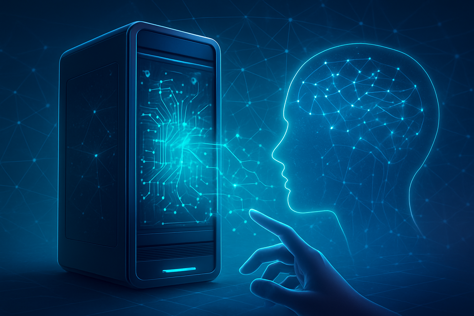
The availability of a dedicated mobile application for ChatGPT marked a significant milestone, moving the powerful large language model from a browser-bound utility to a ubiquitous personal assistant. This move by OpenAI has not only simplified access but also paved the way for more intuitive and integrated AI experiences. As of late 2025, the app is a central hub for cutting-edge AI interactions, from voice commands to multimodal inputs, and its continued development underscores a global trend towards making sophisticated AI tools as common and easy to use as any other smartphone application.
The Technical Blueprint: How ChatGPT Fits in Your Pocket
The journey of the official ChatGPT app began with its iOS debut in May 2023, quickly followed by the Android version in July 2023. This rapid cross-platform deployment ensured broad accessibility from the outset. Further expanding its reach, an official Windows app landed in the Microsoft Store on October 15, 2024, and the innovative ChatGPT Atlas browser, featuring integrated AI, arrived for macOS in October 2025 as a premium offering. The installation process remains remarkably straightforward across mobile platforms: users simply navigate to the Apple App Store or Google Play Store, search for "ChatGPT" (ensuring it's the official OpenAI publication), download, and then log in or sign up with their OpenAI account. A stable internet connection is, of course, a prerequisite for its functionality.
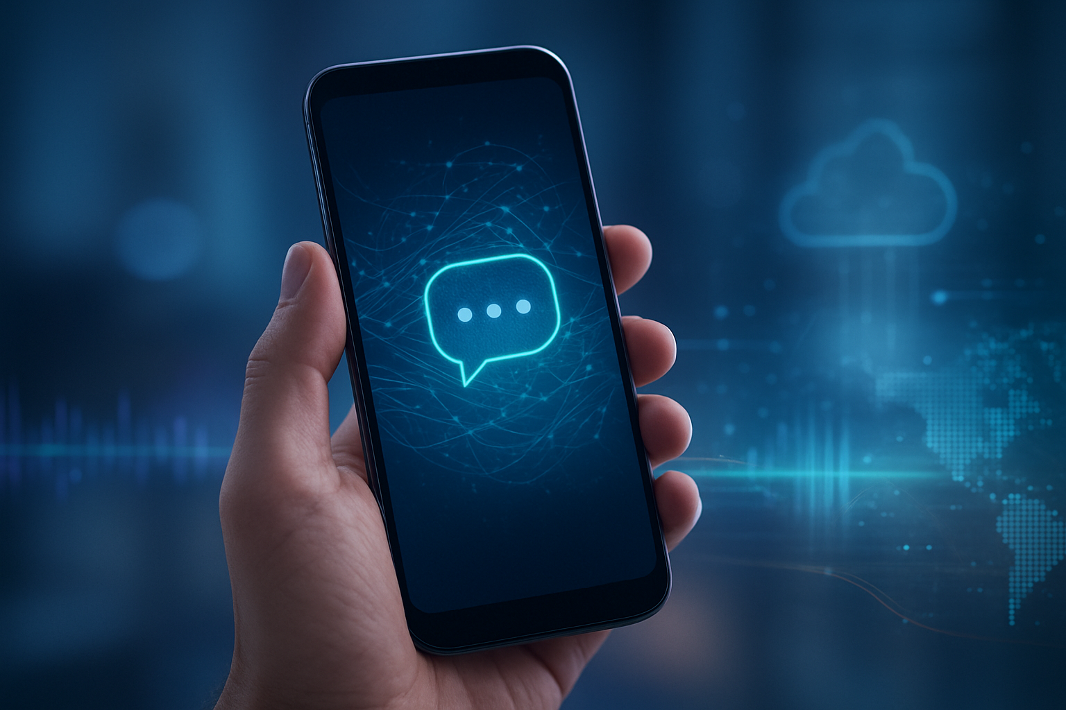
What truly sets the ChatGPT app apart from its earlier web-based iteration and many competitors are its continuously evolving technical capabilities and user experience enhancements. Beyond basic text-based chat, the app leverages Voice Input with Whisper, OpenAI's advanced speech recognition system, allowing for natural spoken queries. This feature, significantly improved in November 2025 to work seamlessly with custom GPTs and offer extensive use for both free and paid users, has revolutionized hands-free interaction. Furthermore, Advanced Voice Mode & Screen Sharing, introduced in June 2025, enables users to upload photos, take pictures directly within chats, and even share their device screen for visual troubleshooting or explanations, turning the AI into a visual and auditory processing powerhouse.
The app's intelligence is also constantly updated. Web Browsing/Search, rolled out as "ChatGPT Search" in October 2024, allows the AI to pull real-time information from the internet, overcoming the limitations of its initial training data cutoff. Its Multimodal Capabilities have blossomed, with premium versions processing and generating content across text, images, video, and audio. Notably, since March 2025, ChatGPT has been capable of generating and transforming images using GPT-4o, and as of November 2025, it incorporates more inline images from the web directly into responses for enhanced visual clarity. The backend models themselves are ever-improving, with GPT-5 updated to GPT-5.1 Instant and GPT-5.1 Thinking in November 2025, offering smarter, more conversational answers and adaptive reasoning for complex tasks. This continuous stream of innovation ensures the mobile app remains at the forefront of AI interaction.
Competitive Ripples: Shifting Sands in the AI Landscape
The pervasive availability and advanced features of the ChatGPT app have sent significant ripples across the AI industry, impacting tech giants and startups alike. OpenAI, as the developer, stands as the primary beneficiary, solidifying its position as a leader in accessible, cutting-edge AI. The broad platform availability also benefits platform owners: Apple (NASDAQ: AAPL) and Google (NASDAQ: GOOGL) gain from increased engagement and potential in-app purchases through their respective app stores, while Microsoft (NASDAQ: MSFT) strengthens its ecosystem with the official Windows app and its deep partnership with OpenAI.
The competitive implications are profound. OpenAI's rapid innovation in mobile AI sets a high bar, compelling other major AI labs and tech companies to accelerate their own mobile-first AI strategies. Companies like Google DeepMind, Meta (NASDAQ: META), and Amazon (NASDAQ: AMZN) are under pressure to match or exceed ChatGPT's multimodal capabilities, seamless user experience, and integration depth. This fosters a healthy but intense competitive environment, driving rapid advancements across the board.
Potential disruption to existing products and services is already evident. Traditional search engines face competition from ChatGPT's conversational web browsing. Personal assistant apps, once cutting-edge, now contend with an AI that offers far more nuanced and intelligent interactions, including advanced voice and visual understanding. The app's integration with tools like Gmail, Google Calendar, and PayPal (NASDAQ: PYPL) for shopping research (as of August and November 2025 respectively) positions it as a central digital hub, potentially siphoning user engagement from specialized applications. OpenAI's strategic advantage lies in its first-mover status in truly democratizing advanced conversational AI, continuously enhancing its market positioning through features like personalized daily updates via ChatGPT Pulse (launched September 2025).
Broader Significance: AI's March Towards Ubiquity
The widespread adoption and continuous evolution of the ChatGPT app signify a critical juncture in the broader AI landscape. It represents a definitive shift towards making sophisticated AI not just a tool for specialists but an integral, intuitive part of everyday digital life for the general public. This move aligns with broader trends of AI democratization and the increasing demand for multimodal interfaces that mimic human communication, allowing interaction through voice, text, and even visual cues. The app's ability to sync conversations across devices and offer features like personalized daily summaries through Pulse highlights a future where AI is deeply integrated and contextually aware across a user's digital footprint.
The impacts are far-reaching. For individuals, it means enhanced productivity, personalized learning experiences, and new avenues for creativity and entertainment. Businesses can leverage its capabilities for customer service, content generation, and data analysis. However, with great power comes potential concerns. Data privacy remains a paramount issue, as users entrust more personal information to the AI. The potential for misinformation or biased outputs, though continuously addressed by OpenAI, requires vigilance. A notable development in December 2025 is OpenAI's plan to implement more comprehensive age-gating, allowing verified adult users to generate and access erotic content under strict safety and moderation guidelines, reflecting the complex ethical landscape AI navigates as it matures.
Comparing this to previous AI milestones, the ChatGPT app's journey is akin to the launch of the first iPhone for mobile internet – it didn't invent the technology, but it made it accessible, intuitive, and ultimately ubiquitous. While previous breakthroughs focused on raw computational power or specific task mastery, the app's significance lies in its user-centric design, multimodal capabilities, and continuous integration into daily workflows. It solidifies AI's transition from a niche technology to a mainstream utility, setting a new benchmark for how humans interact with intelligent systems.
The Horizon: What Comes Next for Mobile AI
Looking ahead, the trajectory of the ChatGPT app points towards even deeper integration, enhanced personalization, and increasingly seamless multimodal interactions. Near-term developments are likely to focus on refining existing features, such as further improvements to voice recognition and generation, expanding the accuracy and scope of web browsing, and integrating with an even wider array of third-party applications and services. The continuous updates to underlying language models, like the recent GPT-5.1 Instant and Thinking, suggest an ongoing pursuit of more nuanced, conversational, and contextually aware AI. We can expect the app to become an even more proactive assistant, anticipating user needs and offering solutions before being explicitly asked.
Potential applications and use cases on the horizon are vast. Imagine an AI that acts as a truly intelligent personal assistant, not just scheduling appointments but proactively suggesting optimal routes based on real-time traffic, drafting emails based on meeting notes, or even helping manage personal finances with integrated payment platforms. In education, it could evolve into an even more personalized tutor, adapting to individual learning styles and providing real-time feedback on complex subjects. For creative professionals, it could serve as a dynamic co-pilot, generating ideas, refining drafts, and even helping to produce multimedia content. The ability to "Call ChatGPT" (a feature launched December 2024 for free for up to 15 minutes per month) hints at a future where AI interaction blurs the lines between digital and traditional communication.
However, challenges remain. Ensuring the ethical deployment of increasingly powerful AI, managing the spread of deepfakes and misinformation, and addressing potential job displacement are critical issues that need continuous attention from developers, policymakers, and society. Experts predict that AI will become an indispensable part of daily digital life, moving beyond a tool to an embedded, ambient intelligence that anticipates and supports human activity. The emphasis will shift from "using AI" to "living with AI," demanding robust frameworks for safety, privacy, and accountability.
A New Era of Interaction: Wrapping Up ChatGPT's Impact
The official ChatGPT mobile app, with its journey from a groundbreaking text interface to a sophisticated multimodal companion, represents a monumental leap in making advanced artificial intelligence accessible to the global populace. Its continuous evolution, marked by features like advanced voice input, screen sharing, real-time web browsing, and deep integrations, underscores a commitment to pushing the boundaries of human-computer interaction. The app's widespread availability across iOS, Android, Windows, and macOS by late 2025 has cemented its status as a pivotal development in AI history, democratizing access to capabilities once confined to research labs.
The significance of this development cannot be overstated. It has not only accelerated the competitive landscape among AI companies but also fundamentally reshaped user expectations for digital assistants. The app's ability to process diverse inputs and provide intelligent, contextual outputs is redefining how we learn, work, and interact with information. While concerns around data privacy and ethical usage persist, OpenAI's proactive steps, such as age-gating for specific content, demonstrate an evolving understanding of its societal responsibilities.
In the coming weeks and months, the tech world will be watching for further enhancements in multimodal AI, deeper personalization features, and expanded integrations that could further embed ChatGPT into the fabric of our digital lives. The long-term impact is clear: the ChatGPT app is a cornerstone in the ongoing transformation of AI from a futuristic concept to an indispensable, everyday reality, promising a future where intelligent assistance is always just a tap or a voice command away.
This content is intended for informational purposes only and represents analysis of current AI developments.
TokenRing AI delivers enterprise-grade solutions for multi-agent AI workflow orchestration, AI-powered development tools, and seamless remote collaboration platforms.
For more information, visit https://www.tokenring.ai/.