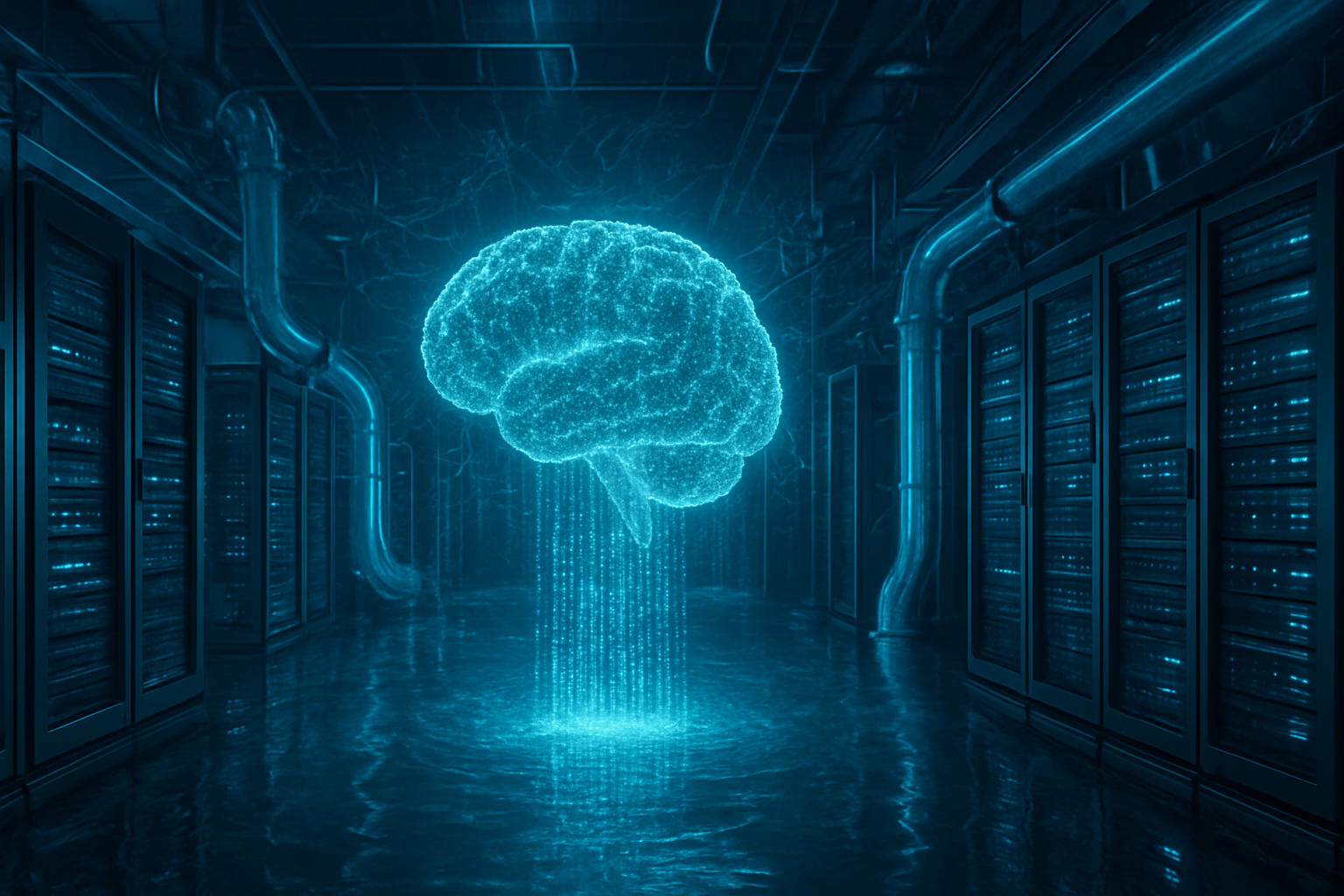
In a definitive signal that the era of the "simple chatbot" is drawing to a close, Databricks has unveiled data showing a massive structural shift in how corporations deploy artificial intelligence. According to the company's "2026 State of AI Agents" report, released yesterday, over 40% of its enterprise customers have moved beyond basic retrieval-augmented generation (RAG) and conversational interfaces to deploy fully autonomous agentic systems. These systems do not merely answer questions; they execute complex, multi-step workflows that span disparate data sources and software applications without human intervention.
The move marks a critical maturation point for generative AI. While 2024 and 2025 were defined by the hype of Large Language Models (LLMs) and the race to implement basic "Ask My Data" tools, 2026 has become the year of the "Compound AI System." By leveraging the Databricks Data Intelligence Platform, organizations are now treating LLMs as the "reasoning engine" within a much larger architecture designed for task execution, leading to a reported 327% surge in multi-agent workflow adoption in just the last six months.
From Chatbots to Supervisors: The Rise of the Compound AI System
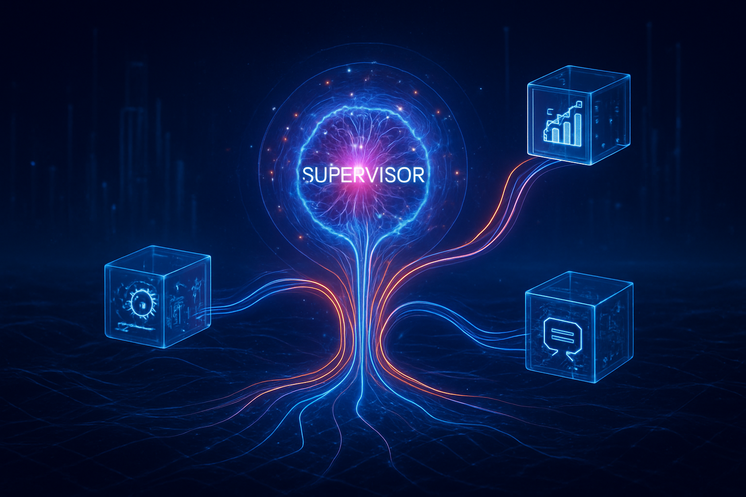
The technical foundation of this shift lies in the transition from single-prompt models to modular, agentic architectures. Databricks’ Mosaic AI has evolved into a comprehensive orchestration environment, moving away from just model training to managing what engineers call "Supervisor Agents." Currently the leading architectural pattern—accounting for 37% of new agentic deployments—a Supervisor Agent acts as a central manager that decomposes a complex user goal into sub-tasks. These tasks are then delegated to specialized "worker" agents, such as SQL agents for data retrieval, document parsers for unstructured text, or API agents for interacting with third-party tools like Salesforce or Jira.
Crucial to this evolution is the introduction of Lakebase, a managed, Postgres-compatible transactional database engine launched by Databricks in late 2025. Unlike traditional databases, Lakebase is optimized for "agentic state management," allowing AI agents to maintain memory and context over long-running workflows that might take minutes or hours to complete. Furthermore, the release of MLflow 3.0 has provided the industry with "agent observability," a set of tools that allow developers to trace the specific "reasoning chains" of an agent. This enables engineers to debug where an autonomous system might have gone off-track, addressing the "black box" problem that previously hindered enterprise-wide adoption.
Industry experts note that this "modular" approach is fundamentally different from the monolithic LLM approach of the past. Instead of asking a single model like GPT-5 to handle everything, companies are using the Mosaic AI Gateway to route specific tasks to the most cost-effective model. A complex reasoning task might go to a frontier model, while a simple data formatting task is handled by a smaller, faster model like Llama 3 or a fine-tuned DBRX variant. This optimization has reportedly reduced operational costs for agentic workflows by nearly 50% compared to early 2025 benchmarks.
The Battle for the Data Intelligence Stack: Microsoft and Snowflake Respond
The rapid adoption of agentic AI on Databricks has intensified the competition among cloud and data giants. Microsoft (NASDAQ: MSFT) has responded by rebranding its AI development suite as Microsoft Foundry, focusing heavily on the "Model Context Protocol" (MCP) to ensure that its own "Agent Mode" for M365 Copilot can interoperate with third-party data platforms. The "co-opetition" between Microsoft and Databricks remains complex; while they compete for the orchestration layer, a deepening integration between Databricks' Unity Catalog and Microsoft Fabric allows enterprises to govern their data in Databricks while utilizing Microsoft's autonomous agents.
Meanwhile, Snowflake (NYSE: SNOW) has doubled down on a "Managed AI" strategy to capture the segment of the market that prefers ease of use over deep customization. With the launch of Snowflake Cortex and the acquisition of the observability firm Observe in early 2026, Snowflake is positioning its platform as the fastest way for a business analyst to trigger an agentic workflow via natural language (AISQL). While Databricks appeals to the "AI Engineer" building custom architectures, Snowflake is targeting the "Data Citizen" who wants autonomous agents embedded directly into their BI dashboards.
The strategic advantage currently appears to lie with platforms that offer robust governance. Databricks’ telemetry indicates that organizations using centralized governance tools like Unity Catalog are deploying AI projects to production 12 times more frequently than those without. This suggests that the "moat" in the AI age is not the model itself, but the underlying data quality and the governance framework that allows an autonomous agent to access that data safely.
The Production Gap and the Era of 'Vibe Coding'
Despite the impressive 40% adoption rate for agentic workflows, the "State of AI" report highlights a persistent "production gap." While 60% of the Fortune 500 are building agentic architectures, only about 19% have successfully deployed them at full enterprise scale. The primary bottlenecks remain security and "agent drift"—the tendency for autonomous systems to become less accurate as the underlying data or APIs change. However, for those who have bridged this gap, the impact is transformative. Databricks reports that agents are now responsible for creating 97% of testing and development environments within its ecosystem, a phenomenon recently dubbed "Vibe Coding," where developers orchestrate high-level intent while agents handle the boilerplate execution.
The broader significance of this shift is a move toward "Intent-Based Computing." In this new paradigm, the user provides a desired outcome (e.g., "Analyze our Q4 churn and implement a personalized discount email campaign for high-risk customers") rather than a series of instructions. This mimics the shift from manual to autonomous driving; the human remains the navigator, but the AI handles the mechanical operations of the "vehicle." Concerns remain, however, regarding the "hallucination of actions"—where an agent might mistakenly delete data or execute an unauthorized transaction—prompting a renewed focus on human-in-the-loop (HITL) safeguards.
Looking Ahead: The Road to 2027
As we move deeper into 2026, the industry is bracing for the next wave of agentic capabilities. Gartner has already predicted that by 2027, 40% of enterprise finance departments will have deployed autonomous agents for auditing and compliance. We expect to see "Agent-to-Agent" (A2A) commerce become a reality, where a procurement agent from one company negotiates directly with a sales agent from another, using standardized protocols to settle terms.
The next major technical hurdle will be "long-term reasoning." Current agents are excellent at multi-step tasks that can be completed in a single session, but "persistent agents" that can manage a project over weeks—checking in on status updates and adjusting goals—are still in the experimental phase. Companies like Amazon (NASDAQ: AMZN) and Google parent Alphabet (NASDAQ: GOOGL) are reportedly working on "world-model" agents that can simulate the outcomes of their actions before executing them, which would significantly reduce the risk of autonomous errors.
A New Chapter in AI History
Databricks' latest data confirms that we have moved past the initial excitement of generative AI and into a more functional, albeit more complex, era of autonomous operations. The transition from 40% of customers using simple chatbots to 40% using autonomous agents represents a fundamental change in the relationship between humans and software. We are no longer just using tools; we are managing digital employees.
The key takeaway for 2026 is that the "Data Intelligence" stack has become the most important piece of real estate in the tech world. As agents become the primary interface for software, the platform that holds the data—and the governance over that data—will hold the power. In the coming months, watch for more aggressive moves into agentic "memory" and "observability" as the industry seeks to make these autonomous systems as reliable as the legacy databases they are quickly replacing.
This content is intended for informational purposes only and represents analysis of current AI developments.
TokenRing AI delivers enterprise-grade solutions for multi-agent AI workflow orchestration, AI-powered development tools, and seamless remote collaboration platforms.
For more information, visit https://www.tokenring.ai/.