The MIT-IBM Watson AI Lab has announced a fundamental breakthrough in Large Language Model (LLM) architecture that addresses one of the most persistent bottlenecks in artificial intelligence: the inability of models to accurately track internal states and variables over long sequences. Known as "PaTH Attention," this new architecture replaces the industry-standard position encoding used by models like GPT-4 with a dynamic, data-dependent mechanism that allows AI to maintain a "positional memory" of every word and action it processes.
This development, finalized in late 2025 and showcased at recent major AI conferences, represents a significant leap in "expressive" AI. By moving beyond the mathematical limitations of current Transformers, the researchers have created a framework that can solve complex logic and state-tracking problems—such as debugging thousands of lines of code or managing multi-step agentic workflows—that were previously thought to be computationally impossible for standard LLMs. The announcement marks a pivotal moment for IBM (NYSE: IBM) as it seeks to redefine the technical foundations of enterprise-grade AI.
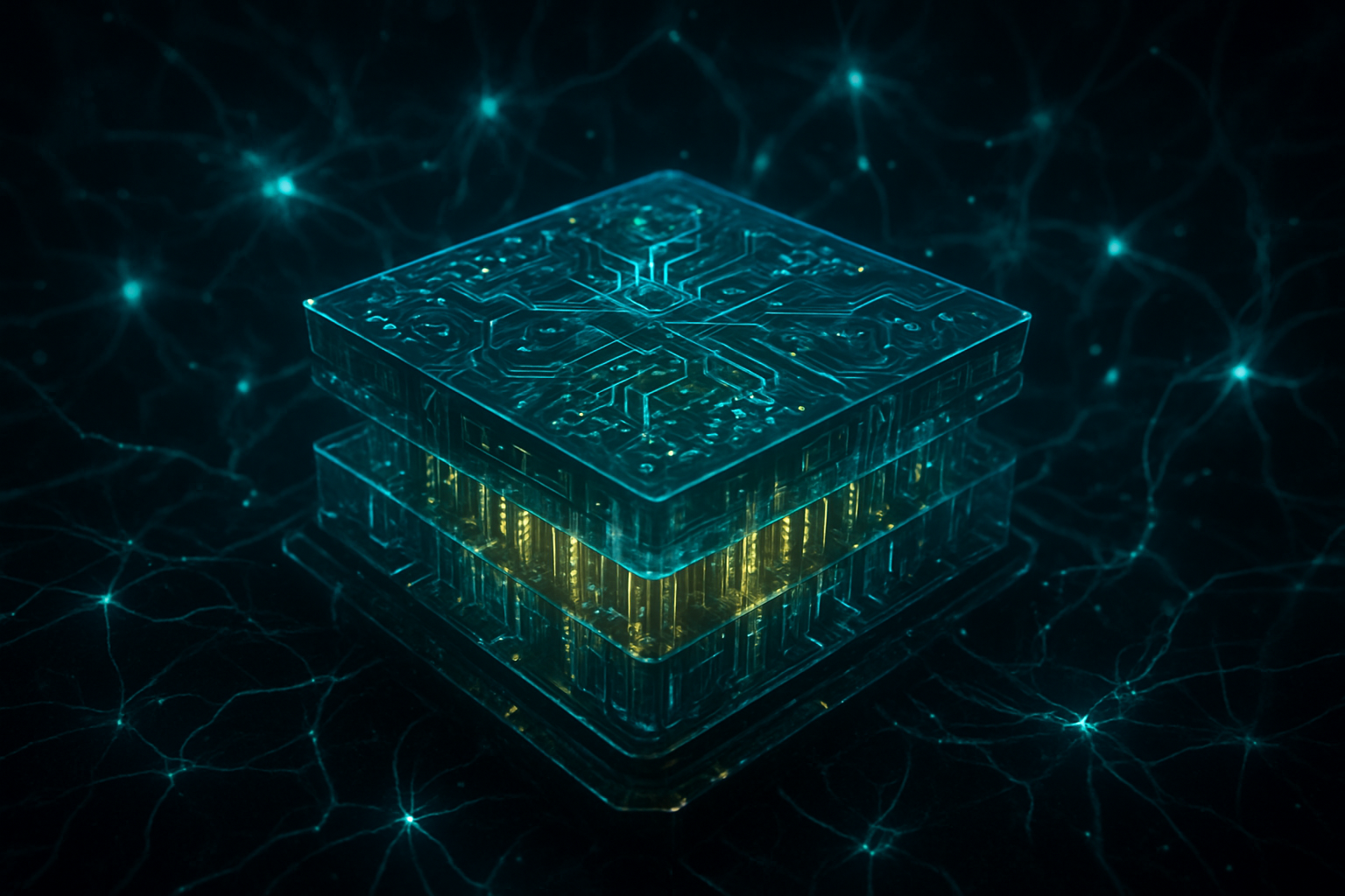
The Science of State: How PaTH Attention Reimagines Memory
At the heart of the MIT-IBM breakthrough is a departure from Rotary Position Encoding (RoPE), the current gold standard used by almost all major AI labs. While RoPE allows models to understand the relative distance between words, it is "data-independent," meaning the way a model perceives position is fixed regardless of what the text actually says. The PaTH architecture—short for Position Encoding via Accumulating Householder Transformations—replaces these static rotations with content-aware reflections. As the model reads a sequence, each word produces a unique "Householder transformation" that adjusts the model’s internal state, effectively creating a path of accumulated memory that evolves with the context.
This shift provides the model with what researchers call "NC1-complete" expressive power. In the world of computational complexity, standard Transformers are limited to a class known as TC0, which prevents them from solving certain types of deep, nested logical problems no matter how many parameters they have. By upgrading to the NC1 class, the PaTH architecture allows LLMs to track state changes with the precision of a traditional computer program while maintaining the creative flexibility of a neural network. This is particularly evident in the model's performance on the "RULER" benchmark, where it maintained nearly 100% accuracy in retrieving and reasoning over information buried in contexts of over 64,000 tokens.
To ensure this new complexity didn't come at the cost of speed, the team—which included collaborators from Microsoft (NASDAQ: MSFT) and Stanford—developed a hardware-efficient training algorithm. Using a "compact representation" of these transformations, the researchers achieved parallel processing speeds comparable to FlashAttention. Furthermore, the architecture is often paired with a "FoX" (Forgetting Transformer) mechanism, which uses data-dependent "forget gates" to prune irrelevant information, preventing the model’s memory from becoming cluttered during massive data processing tasks.
Shifting the Power Balance in the AI Arms Race
The introduction of PaTH Attention places IBM in a strategic position to challenge the dominance of specialized AI labs like OpenAI and Anthropic. While the industry has largely focused on "scaling laws"—simply making models larger to improve performance—IBM's work suggests that architectural efficiency may be the true frontier for the next generation of AI. For enterprises, this means more reliable "Agentic AI" that can navigate complex business logic without "hallucinating" or losing track of its original goals mid-process.
Tech giants like Google (NASDAQ: GOOGL) and Meta (NASDAQ: META) are likely to take note of this shift, as the move toward NC1-complete architectures could disrupt the current reliance on massive, power-hungry clusters for long-context reasoning. Startups specializing in AI-driven software engineering and legal discovery also stand to benefit significantly; a model that can track variable states through a million lines of code or maintain a consistent "state of mind" throughout a complex litigation file is a massive competitive advantage.
Furthermore, the collaboration with Microsoft researchers hints at a broader industry recognition that the Transformer, in its current form, may be reaching its ceiling. By open-sourcing parts of the PaTH research, the MIT-IBM Watson AI Lab is positioning itself as the architect of the "Post-Transformer" era. This move could force other major players to accelerate their own internal architecture research, potentially leading to a wave of "hybrid" models that combine the best of attention mechanisms with these more expressive state-tracking techniques.
The Dawn of Truly Agentic Intelligence
The wider significance of this development lies in its implications for the future of autonomous AI agents. Current AI "agents" often struggle with "state drift," where the model slowly loses its grip on the initial task as it performs more steps. By mathematically guaranteeing better state tracking, PaTH Attention paves the way for AI that can function as true digital employees, capable of executing long-term projects that require memory of past decisions and their consequences.
This milestone also reignites the debate over the theoretical limits of deep learning. For years, critics have argued that neural networks are merely "stochastic parrots" incapable of true symbolic reasoning. The MIT-IBM work provides a counter-argument: by increasing the expressive power of the architecture, we can bridge the gap between statistical pattern matching and logical state-tracking. This brings the industry closer to a synthesis of neural and symbolic AI, a "holy grail" for many researchers in the field.
However, the leap in expressivity also raises new concerns regarding safety and interpretability. A model that can maintain more complex internal states is inherently harder to "peek" into. As these models become more capable of tracking their own internal logic, the challenge for AI safety researchers will be to ensure that these states remain transparent and aligned with human intent, especially as the models are deployed in critical infrastructure like financial trading or healthcare management.
What’s Next: From Research Paper to Enterprise Deployment
In the near term, experts expect to see the PaTH architecture integrated into IBM’s watsonx platform, providing a specialized "Reasoning" tier for corporate clients. This could manifest as highly accurate code-generation tools or document analysis engines that outperform anything currently on the market. We are also likely to see "distilled" versions of these expressive architectures that can run on consumer-grade hardware, bringing advanced state-tracking to edge devices and personal assistants.
The next major challenge for the MIT-IBM team will be scaling these NC1-complete models to the trillion-parameter level. While the hardware-efficient algorithms are a start, the sheer complexity of accumulated transformations at that scale remains an engineering hurdle. Predictions from the research community suggest that 2026 will be the year of "Architectural Diversification," where we move away from a one-size-fits-all Transformer approach toward specialized architectures like PaTH for logic-heavy tasks.
Final Thoughts: A New Foundation for AI
The work coming out of the MIT-IBM Watson AI Lab marks a fundamental shift in how we build the "brains" of artificial intelligence. By identifying and solving the expressive limitations of the Transformer, researchers have opened the door to a more reliable, logical, and "memory-capable" form of AI. The transition from TC0 to NC1 complexity might sound like an academic nuance, but it is the difference between an AI that merely predicts the next word and one that truly understands the state of the world it is interacting with.
As we move deeper into 2026, the success of PaTH Attention will be measured by its adoption in the wild. If it can deliver on its promise of solving the "memory crisis" in AI, it may well go down in history alongside the original 2017 "Attention is All You Need" paper as a cornerstone of the modern era. For now, all eyes are on the upcoming developer previews from IBM and its partners to see how these mathematical breakthroughs translate into real-world performance.
This content is intended for informational purposes only and represents analysis of current AI developments.
TokenRing AI delivers enterprise-grade solutions for multi-agent AI workflow orchestration, AI-powered development tools, and seamless remote collaboration platforms.
For more information, visit https://www.tokenring.ai/.