Category: Uncategorized

  • The RISC-V Revolution: Breaking the ARM Monopoly in 2026

    The RISC-V Revolution: Breaking the ARM Monopoly in 2026

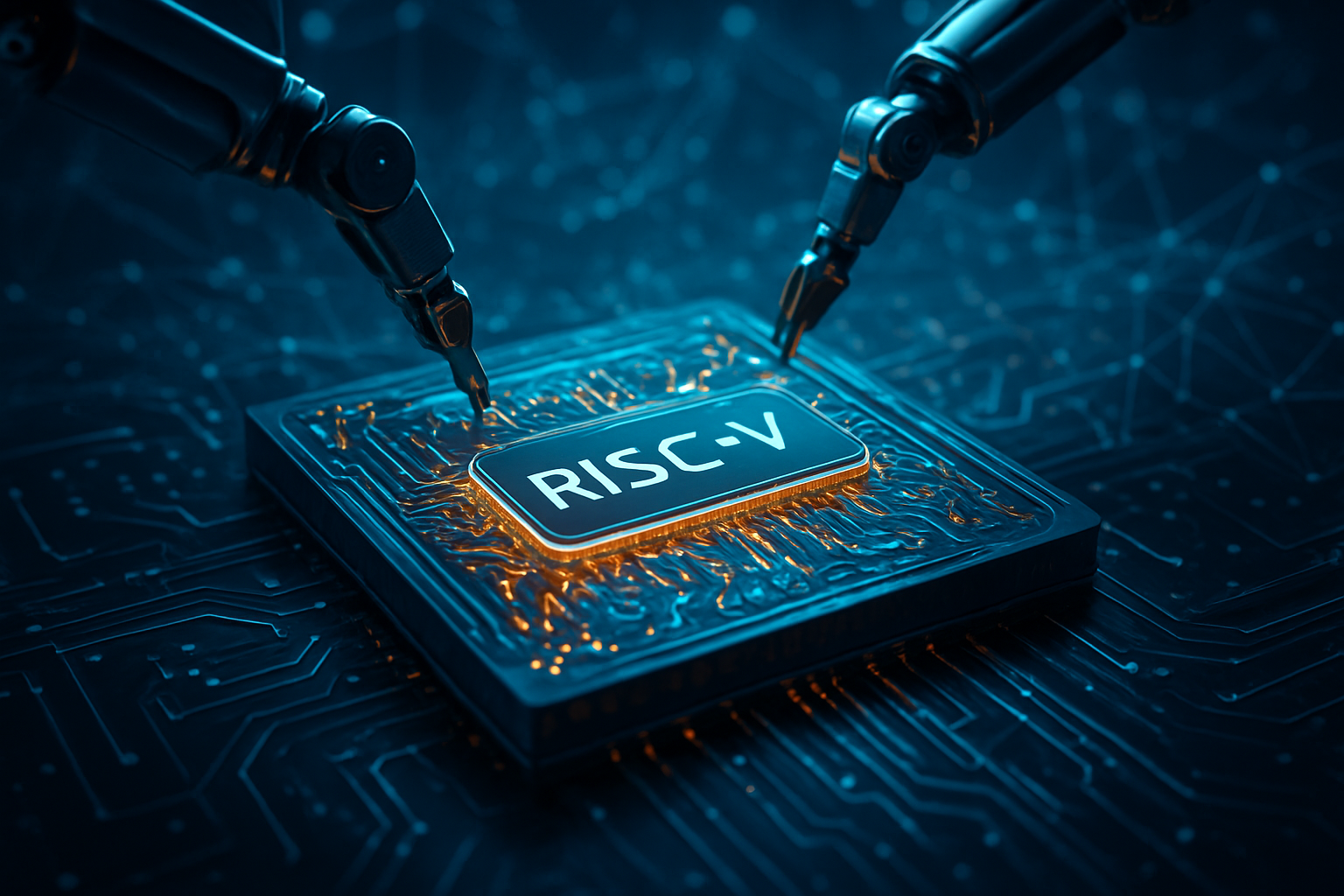
    The high-performance computing landscape has reached a historic inflection point in early 2026, as the open-source RISC-V architecture officially shatters the long-standing duopoly of ARM and x86. What began a decade ago as an academic project at UC Berkeley has matured into a formidable industrial force, driven by a global surge in demand for "architectural sovereignty." The catalyst for this shift is the arrival of server-class RISC-V processors that finally match the performance of industry leaders, coupled with a massive migration by tech giants seeking to escape the escalating licensing costs of traditional silicon.

    The move marks a fundamental shift in the power dynamics of the semiconductor industry. For the first time, companies like Qualcomm (NASDAQ: QCOM) and Meta (NASDAQ: META) are not merely consumers of chip designs but are becoming the architects of their own bespoke silicon ecosystems. By leveraging the modularity of RISC-V, these firms are bypassing the restrictive "ARM Tax" and building specialized processors tailored specifically for generative AI, high-density cloud computing, and low-power wearable devices.

    The Dawn of the Server-Class RISC-V Era

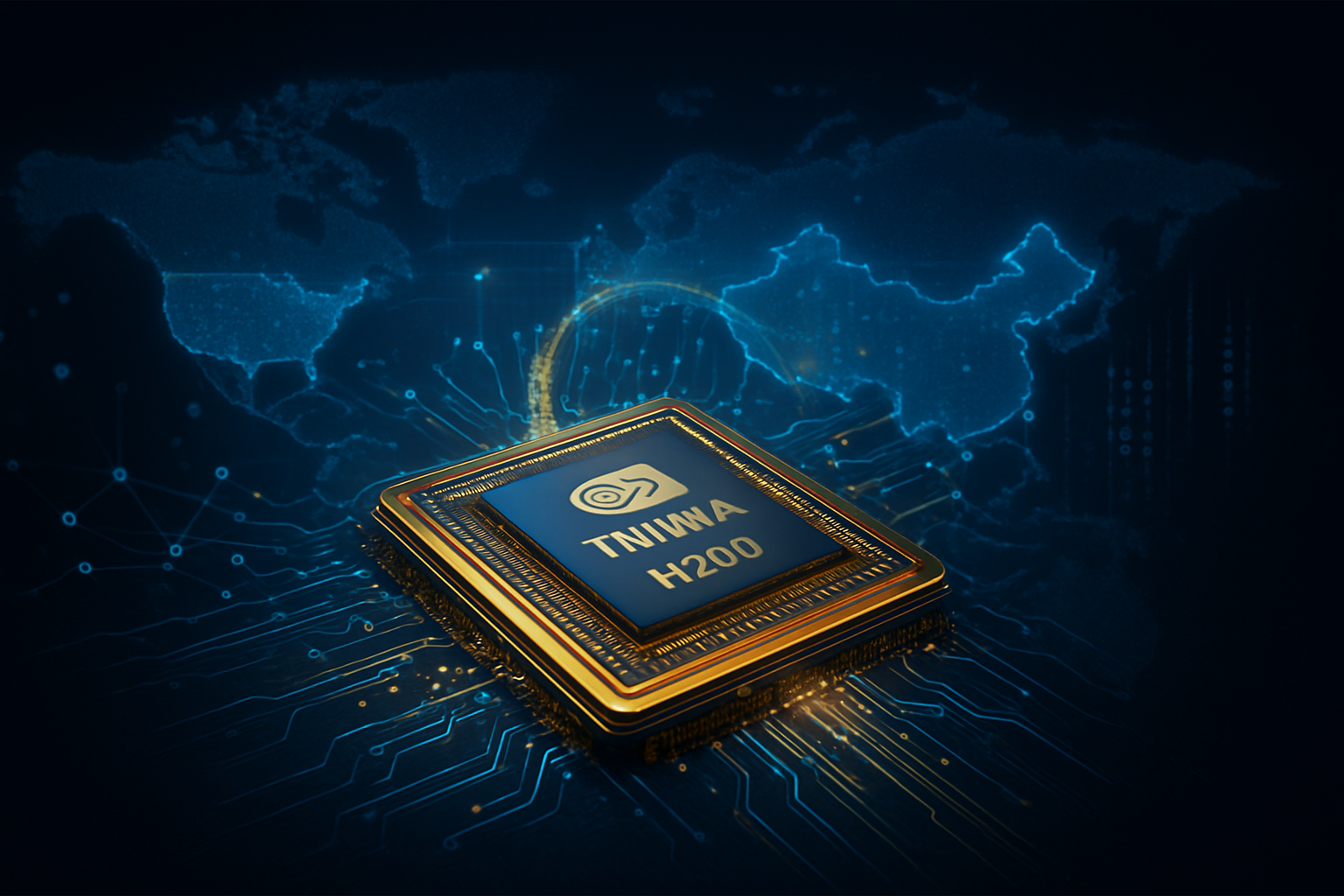
    The technical barrier that previously kept RISC-V confined to simple microcontrollers has been decisively breached. Leading the charge is SpacemiT, which recently debuted its VitalStone V100 server processor. The V100 is a 64-core powerhouse built on a 12nm process, featuring the proprietary X100 "AI Fusion" core. This architecture utilizes a 12-stage out-of-order pipeline that is fully compliant with the RVA23 profile, the new 2026 standard that ensures enterprise-grade features like virtualization and high-speed I/O management.

    Performance benchmarks reveal that the X100 core achieves parity with the ARM (NASDAQ: ARM) Neoverse V1 and Advanced Micro Devices (NASDAQ: AMD) Zen 2 architectures in integer performance, while significantly outperforming them in specialized AI workloads. SpacemiT’s "AI Fusion" technology allows for a 20x performance increase in INT8 matrix multiplications compared to standard SIMD implementations. This allows the V100 to handle Large Language Model (LLM) inference directly on the CPU, reducing the need for expensive, power-hungry external accelerators in edge-server environments.

    This leap in capability is supported by the ratification of the RISC-V Server Platform Specification, which has finally solved the "software gap." As of 2026, major enterprise operating systems including Red Hat and Ubuntu run natively on RISC-V with UEFI and ACPI support. This means that data center operators can now swap x86 or ARM instances for RISC-V servers without rewriting their entire software stack, a breakthrough that industry experts are calling the "Linux moment" for hardware.

    Strategic Sovereignty: Qualcomm and Meta Lead the Exodus

    The business case for RISC-V has become undeniable for the world's largest tech companies. Qualcomm has fundamentally restructured its roadmap to prioritize RISC-V, largely as a hedge against its volatile legal relationship with ARM. By early 2026, Qualcomm’s Snapdragon Wear platform has fully transitioned to RISC-V cores. In a landmark collaboration with Google (NASDAQ: GOOGL), the latest generation of Wear OS devices now runs on custom RISC-V silicon, allowing Qualcomm to optimize power efficiency for "always-on" AI features without paying per-core royalties to ARM.

    Furthermore, Qualcomm’s $2.4 billion acquisition of Ventana Micro Systems in late 2025 has provided it with high-performance RISC-V chiplets capable of competing in the data center. This move allows Qualcomm to offer a full-stack solution—from the wearable device to the private AI cloud—all running on a unified, royalty-free architecture. This vertical integration provides a massive strategic advantage, as it enables the addition of custom instructions that ARM’s standard licensing models would typically prohibit.

    Meta has followed a similar path, driven by the astronomical costs of running Llama-based AI models at scale. The company’s MTIA (Meta Training and Inference Accelerator) chips now utilize RISC-V cores for complex control logic. Meta’s acquisition of the RISC-V startup Rivos has allowed it to build a custom CPU that acts as a "traffic cop" for its AI clusters. By designing its own RISC-V silicon, Meta estimates it will save over $500 million annually in licensing fees and power efficiencies, while simultaneously optimizing its hardware for the specific mathematical requirements of its proprietary AI models.

    A Geopolitical and Economic Paradigm Shift

    The rise of RISC-V is more than just a technical or corporate trend; it is a geopolitical necessity in the 2026 landscape. Because the RISC-V International organization is based in Switzerland, the architecture is largely insulated from the trade wars and export restrictions that have plagued US and UK-based technologies. This has made RISC-V the default choice for emerging markets and Chinese firms like Alibaba (NYSE: BABA), which has integrated RISC-V into its XuanTie series of cloud processors.

    The formation of the Quintauris alliance—founded by Qualcomm, Infineon (OTC: IFNNY), and other automotive giants—has further stabilized the ecosystem. Quintauris acts as a clearinghouse for reference architectures, ensuring that RISC-V implementations remain compatible and secure. This collective approach prevents the "fragmentation" that many feared would kill the open-source hardware movement. Instead, it has created a "Lego-like" environment where companies can mix and match chiplets from different vendors, significantly lowering the barrier to entry for silicon startups.

    However, the rapid growth of RISC-V has not been without controversy. Traditional incumbents like Intel (NASDAQ: INTC) have been forced to pivot, with Intel Foundry now aggressively marketing its ability to manufacture RISC-V chips for third parties. This creates a strange paradox where the older giants are now facilitating the growth of the very architecture that seeks to replace their proprietary instruction sets.

    The Road Ahead: From Servers to the Desktop

    As we look toward the remainder of 2026 and into 2027, the focus is shifting toward the consumer PC and high-end mobile markets. While RISC-V has conquered the server and the wearable, the "Final Boss" remains the high-end smartphone and the laptop. Expert analysts predict that the first high-performance RISC-V "AI PC" will debut by late 2026, likely powered by a collaboration between NVIDIA (NASDAQ: NVDA) and a RISC-V core provider, aimed at the burgeoning creative professional market.

    The primary challenge remaining is the "Long Tail" of legacy software. While cloud-native applications and AI models port easily to RISC-V, decades of Windows-based software still require x86 compatibility. However, with the maturation of high-speed binary translation layers—similar to Apple's (NASDAQ: AAPL) Rosetta 2—the performance penalty for running legacy apps on RISC-V is shrinking. The industry is watching closely to see if Microsoft will release a "Windows on RISC-V" edition to rival its ARM-based offerings.

    A New Era of Silicon Innovation

    The RISC-V revolution of 2026 represents the ultimate democratization of hardware. By removing the gatekeepers of the instruction set, the industry has unleashed a wave of innovation that was previously stifled by licensing costs and rigid design templates. The success of SpacemiT’s server chips and the strategic pivots by Qualcomm and Meta prove that the world is ready for a modular, open-source future.

    The takeaway for the industry is clear: the monopoly of the proprietary ISA is over. In its place is a vibrant, competitive landscape where performance is dictated by architectural ingenuity rather than licensing clout. In the coming months, keep a close eye on the mobile sector; as soon as a flagship RISC-V smartphone hits the market, the transition will be complete, and the ARM era will officially pass into the history books.


    This content is intended for informational purposes only and represents analysis of current AI developments.

    TokenRing AI delivers enterprise-grade solutions for multi-agent AI workflow orchestration, AI-powered development tools, and seamless remote collaboration platforms.
    For more information, visit https://www.tokenring.ai/.

  • India’s Silicon Shield: How the Tata-ROHM Alliance is Rewriting the Global Semiconductor and AI Power Map

    India’s Silicon Shield: How the Tata-ROHM Alliance is Rewriting the Global Semiconductor and AI Power Map

    As of January 26, 2026, the global semiconductor landscape has undergone a tectonic shift. What was once a policy-driven ambition for the Indian subcontinent has transformed into a tangible, high-output reality. At the center of this transformation is a pivotal partnership between Tata Electronics and ROHM Co., Ltd. (TYO: 6963), a Japanese pioneer in power and analog semiconductors. This alliance, focusing on the production of automotive-grade power MOSFETs (Metal-Oxide-Semiconductor Field-Effect Transistors), marks a critical milestone in India’s bid to offer a robust, democratic alternative to China’s long-standing dominance in mature-node manufacturing.

    The significance of this development extends far beyond simple hardware assembly. By localizing the production of high-current power management components, India is securing the physical backbone required for the next generation of AI-driven mobility and industrial automation. As the "China+1" strategy matures into a standard operating procedure for Western tech giants, the Tata-ROHM partnership stands as the first major proof of concept for India’s Semiconductor Mission (ISM) 2.0, successfully bridging the gap between design expertise and high-volume fabrication.

    Technical Prowess: Powering the Edge AI Revolution

    The technical centerpiece of the Tata-ROHM collaboration is the commercial rollout of an automotive-grade N-channel silicon MOSFET, specifically engineered for the rigorous demands of electric vehicles (EVs) and smart energy systems. Boasting a voltage rating of 100V and a current capacity of 300A, these chips utilize a TOLL (Transistor Outline Leadless) package. This modern surface-mount design is critical for high power density, offering superior thermal efficiency and lower parasitic inductance compared to traditional packaging. In the context of early 2026, where "Edge AI" in vehicles requires massive real-time processing, these power chips ensure that the high-current demands of onboard Neural Processing Units (NPUs) are met without compromising vehicle range or safety.

    This development is inextricably linked to the progress of India’s first mega-fab in Dholera, Gujarat—a $11 billion joint venture between Tata and Powerchip Semiconductor Manufacturing Corp (PSMC). As of this month, the Dholera facility has successfully completed high-volume trial runs using 300mm (12-inch) wafers. While the industry’s "bleeding edge" focuses on sub-5nm nodes, Tata’s strategic focus on the 28nm, 40nm, and 90nm "workhorse" nodes is a calculated move. These nodes are the essential foundations for Power Management ICs (PMICs), display drivers, and microcontrollers. Initial reactions from the industry have been overwhelmingly positive, with experts noting that India has bypassed the "learning curve" typically associated with greenfield fabs by integrating ROHM's established design IP directly into Tata’s manufacturing workflow.

    Market Impact: Navigating the 'China+1' Paradigm

    The market implications of this partnership are profound, particularly for the automotive and AI hardware sectors. Tata Motors (NSE: TATAMOTORS) and other global OEMs stand to benefit immensely from a shortened, more resilient supply chain that bypasses the geopolitical volatility associated with East Asian hubs. By establishing a reliable source of AEC-Q101 qualified semiconductors on Indian soil, the partnership offers a strategic hedge against potential sanctions or trade disruptions involving Chinese manufacturers like BYD (HKG: 1211).

    Furthermore, the involvement of Micron Technology (NASDAQ: MU)—whose Sanand facility reached full-scale commercial production in February 2026—and CG Power & Industrial Solutions (NSE: CGPOWER) creates a synergistic cluster. This ecosystem allows for "full-stack" manufacturing, where memory modules from Micron can be paired with power management chips from Tata-ROHM and logic chips from the Dholera fab. This vertical integration provides India with a unique competitive edge in the mid-range semiconductor market, which currently accounts for roughly 75% of global chip volume. Tech giants looking to diversify their hardware sourcing now view India not just as a consumer market, but as a critical export hub for the global AI and EV supply chains.

    The Geopolitical and AI Landscape: Beyond the Silicon

    The rise of the Tata-ROHM alliance must be viewed through the lens of the U.S.-India TRUST (Transforming the Relationship Utilizing Strategic Technology) initiative. This framework has paved the way for India to join the "Pax Silica" alliance, a group of nations committed to securing "trusted" silicon supply chains. For the global AI community, this means that the hardware required for "Sovereign AI"—data centers and AI-enabled infrastructure built within national borders—now has a secondary, reliable point of origin.

    In the data center space, the demand for Silicon Carbide (SiC) and Gallium Nitride (GaN) is exploding. These "Wide-Bandgap" materials are essential for the high-efficiency power units required by massive AI server racks featuring NVIDIA (NASDAQ: NVDA) Blackwell-architecture chips. The Tata-ROHM roadmap already signals a transition to SiC wafer production by 2027. By addressing the thermal and power density challenges of AI infrastructure, India is positioning itself as an indispensable partner in the global race for AI supremacy, ensuring that the energy-hungry demands of large language models (LLMs) are met by more efficient, locally-produced hardware.

    Future Horizons: From 28nm to the Bleeding Edge

    Looking ahead, the next 24 to 36 months will be decisive. Near-term expectations include the first commercial shipment of "Made in India" silicon from the Dholera fab by December 2026. However, the roadmap doesn't end at 28nm. Plans are already in motion for "Fab 2," which aims to target 14nm and eventually 7nm nodes to cater to the smartphone and high-performance computing (HPC) markets. The integration of advanced lithography systems from ASML (NASDAQ: ASML) into Indian facilities suggests that the technological ceiling is rapidly rising.

    The challenges remain significant: maintaining a consistent power supply, managing the high water-usage requirements of fabs, and scaling the specialized workforce. However, the Gujarat government's rapid infrastructure build-out—including thousands of residential units for semiconductor staff—demonstrates a level of political will rarely seen in industrial history. Analysts predict that by 2030, India could command a 10% share of the global semiconductor market, effectively neutralizing the risk of a single-point failure in the global electronics supply chain.

    A New Era for Global Manufacturing

    In summary, the partnership between Tata Electronics and ROHM is more than a corporate agreement; it is the cornerstone of a new global order in technology manufacturing. It signifies India's successful transition from a software-led economy to a hardware powerhouse capable of producing the most complex components of the modern age. The key takeaway for investors and industry leaders is clear: the semiconductor center of gravity is shifting.

    As we move deeper into 2026, the success of the Tata-ROHM venture will serve as a bellwether for India’s long-term semiconductor goals. The convergence of AI infrastructure needs, automotive electrification, and geopolitical realignments has created a "perfect storm" that India is now uniquely positioned to navigate. For the global tech industry, the emergence of this Indian silicon shield provides a much-needed layer of resilience in an increasingly uncertain world.


    This content is intended for informational purposes only and represents analysis of current AI developments.

    TokenRing AI delivers enterprise-grade solutions for multi-agent AI workflow orchestration, AI-powered development tools, and seamless remote collaboration platforms.
    For more information, visit https://www.tokenring.ai/.

  • NVIDIA H200s Cleared for China: Inside the Trump Administration’s Bold High-Stakes Tech Thaw

    NVIDIA H200s Cleared for China: Inside the Trump Administration’s Bold High-Stakes Tech Thaw

    In a move that has sent shockwaves through both Silicon Valley and Beijing, the Trump administration has officially authorized the export of NVIDIA H200 GPU accelerators to the Chinese market. The decision, finalized in late January 2026, marks a dramatic reversal of the multi-year "presumption of denial" policy that had effectively crippled the sales of high-end American AI hardware to China. By replacing blanket bans with a transactional, security-monitored framework, the U.S. government aims to reassert American influence over global AI ecosystems while capturing significant federal revenue from the world’s second-largest economy.

    The policy shift is being hailed by industry leaders as a pragmatic "thaw" in tech relations, though it comes with a complex web of restrictions that distinguish it from the unrestricted trade of the past decade. For NVIDIA (NASDAQ: NVDA), the announcement represents a lifeline for its Chinese business, which had previously been relegated to selling "degraded" or lower-performance chips like the H20 to comply with strict 2023 and 2024 export controls. Under the new regime, the H200—one of the most powerful AI training and inference chips currently in production—will finally be available to vetted Chinese commercial entities.

    Advanced Silicon and the "Vulnerability Screening" Mandate

    The technical specifications of the NVIDIA H200 represent a massive leap forward for the Chinese AI industry. Built on the Hopper architecture, the H200 is the first GPU to feature HBM3e memory, delivering 141GB of capacity and 4.8 TB/s of memory bandwidth. Compared to the H100, the H200 offers nearly double the inference performance for large language models (LLMs) like Llama 3 or GPT-4. This bandwidth is the critical factor in modern AI scaling, and its availability in China is expected to dramatically shorten the training cycles for domestic Chinese models which had been stagnating under previous hardware constraints.

    To maintain a strategic edge, the U.S. Department of Commerce’s Bureau of Industry and Security (BIS) has introduced a new "regulatory sandwich." Under the January 13, 2026 ruling, chips are permitted for export only if their Total Processing Performance (TPP) remains below 21,000 and DRAM bandwidth stays under 6,500 GB/s. While the H200 fits within these specific bounds, the administration has eliminated the practice of "binning" or hardware-level performance capping for the Chinese market. Instead, the focus has shifted to who is using the chips and how they are being deployed.

    A key technical innovation in this policy is the "U.S. First" testing protocol. Before any H200 units are shipped to China, they must first be imported from manufacturing hubs into specialized American laboratories. There, they undergo "vulnerability screening" and technical verification to ensure no unauthorized firmware modifications have been made. This allows the U.S. government to maintain a literal hands-on check on the hardware before it enters the Chinese supply chain, a logistical hurdle that experts say is unprecedented in the history of semiconductor trade.

    Initial reactions from the AI research community have been cautiously optimistic. While researchers at institutions like Tsinghua University welcome the performance boost, there is lingering skepticism regarding the mandatory U.S. testing phase. Industry analysts note that this requirement could introduce a 4-to-6 week delay in the supply chain. However, compared to the alternative—developing sovereign silicon that still lags generations behind NVIDIA—most Chinese tech giants see this as a necessary price for performance.

    Revenue Levies and the Battle for Market Dominance

    The financial implications for NVIDIA are profound. Before the 2023 restrictions, China accounted for approximately 20% to 25% of NVIDIA’s data center revenue. This figure had plummeted as Chinese firms were forced to choose between underpowered U.S. chips and domestic alternatives. With the H200 now on the table, analysts predict a massive surge in capital expenditure from Chinese "hyperscalers" such as Alibaba (NYSE: BABA), Tencent (HKG: 0700), and Baidu (NASDAQ: BIDU). These companies have been eager to upgrade their aging infrastructure to compete with Western AI capabilities.

    However, the "Trump Thaw" is far from a free pass. The administration has imposed a mandatory 25% "revenue levy" on all H200 sales to China, structured as a Section 232 national security tariff. This ensures that the U.S. Treasury benefits directly from every transaction. Additionally, NVIDIA is subject to volume caps: the total number of H200s exported to China cannot exceed 50% of the volume sold to U.S. domestic customers. This "America First" ratio is designed to ensure that the U.S. always maintains a larger, more advanced install base of AI compute power.

    The move also places intense pressure on Advanced Micro Devices (NASDAQ: AMD), which has been seeking its own licenses for the Instinct MI325X series. As the market opens, a new competitive landscape is emerging where U.S. companies are not just competing against each other, but against the rising tide of Chinese domestic competitors like Huawei. By allowing the H200 into China, the U.S. is effectively attempting to "crowd out" Huawei’s Ascend 910C chips, making it harder for Chinese firms to justify the switch to a domestic ecosystem that remains more difficult to program for.

    Strategic advantages for ByteDance—the parent company of TikTok—are also in the spotlight. ByteDance has historically been one of NVIDIA's largest customers in Asia, using GPUs for its massive recommendation engines and generative AI projects. The ability to legally procure H200s gives ByteDance a clear path to maintaining its global competitive edge, provided it can navigate the stringent end-user vetting processes required by the new BIS rules.

    The Geopolitical "AI Overwatch" and a Fragile Thaw

    The broader significance of this decision cannot be overstated. It signals a shift in the U.S. strategy from total containment to a "managed dependency." By allowing China to buy NVIDIA’s second-best hardware (with the newer Blackwell architecture still largely restricted), the U.S. keeps the Chinese tech sector tethered to American software stacks like CUDA. Experts argue that if China were forced to fully decouple, they would eventually succeed in building a parallel, independent tech ecosystem. This policy is an attempt to delay that "Sputnik moment" indefinitely.

    This strategy has not been without fierce domestic opposition. On January 21, 2026, the House Foreign Affairs Committee advanced the "AI Overwatch Act" (H.R. 6875), a bipartisan effort to grant Congress the power to veto specific export licenses. Critics of the administration, including many "China hawks," argue that the H200 is too powerful to be exported safely. They contend that the 25% tariff is a "pay-to-play" scheme that prioritizes corporate profits and short-term federal revenue over long-term national security, fearing that the hardware will inevitably be diverted to military AI projects.

    Comparing this to previous AI milestones, such as the 2022 ban on the A100, the current situation represents a much more transactional approach to geopolitics. The administration's "AI and Crypto Czar," David Sacks, has defended the policy by stating that the U.S. must lead the global AI ecosystem through engagement rather than isolation. The "thaw" is seen as a way to lower the temperature on trade relations while simultaneously building a massive federal war chest funded by Chinese tech spending.

    Beijing’s response has been characteristically measured but complex. While the Ministry of Industry and Information Technology (MIIT) has granted "in-principle" approval for firms to order H200s, they have also reportedly mandated that for every U.S. chip purchased, a corresponding investment must be made in domestic silicon. This "one-for-one" quota system indicates that while China is happy to have access to NVIDIA’s power, it remains fully committed to its long-term goal of self-reliance.

    Future Developments: Blackwell and the Parity Race

    As we look toward the remainder of 2026, the primary question is whether this policy will extend to NVIDIA’s next-generation Blackwell architecture. Currently, the B200 remains restricted, keeping the "performance gap" between the U.S. and China at approximately 12 to 18 months. However, if the H200 export experiment is deemed a financial and security success, there is already talk in Washington of a "Blackwell Lite" variant being introduced by 2027.

    The near-term focus will be on the logistical execution of the "vulnerability screening" labs. If these facilities become a bottleneck, it could lead to renewed friction between the White House and the tech industry. Furthermore, the world will be watching to see if other nations, particularly in the Middle East and Southeast Asia, demand similar "case-by-case" license review policies to access the highest tiers of American compute power.

    Predicting the next moves of the Chinese "national champions" is also vital. With access to H200s, will Alibaba and Baidu finally reach parity with U.S.-based models like Claude or Gemini? Or will the U.S. domestic volume caps ensure that American labs always have a two-to-one advantage in raw compute? Most experts believe that while the H200 will prevent a total collapse of the Chinese AI sector, the structural advantages of the U.S. ecosystem—combined with the new 25% "AI Tax"—will keep the American lead intact.

    A New Chapter in the Silicon Cold War

    The approval of NVIDIA H200 exports to China is a defining moment in the history of artificial intelligence and international trade. It represents a pivot from the "small yard, high fence" strategy toward a more dynamic "toll-booth" model. By allowing high-performance hardware to flow into China under strict supervision and high taxation, the Trump administration is betting that economic interdependency can be used as a tool for national security rather than a vulnerability.

    In the coming weeks, the industry will watch closely for the first confirmed shipments of H200s landing in Shanghai and the resulting benchmarks from Chinese AI labs. The success or failure of this policy will likely dictate the trajectory of U.S.-China relations for the rest of the decade. If the H200s are used to create breakthroughs that threaten U.S. interests, the "AI Overwatch Act" will almost certainly be invoked to shut the gates once again.

    Ultimately, the H200 export decision is a high-stakes gamble. It provides NVIDIA and the U.S. Treasury with a massive financial windfall while offering China the tools it needs to stay in the AI race. Whether this leads to a stable "technological co-existence" or merely fuels the next phase of an escalating AI arms race remains the most critical question of 2026.


    This content is intended for informational purposes only and represents analysis of current AI developments.

    TokenRing AI delivers enterprise-grade solutions for multi-agent AI workflow orchestration, AI-powered development tools, and seamless remote collaboration platforms.
    For more information, visit https://www.tokenring.ai/.

  • The Memory Wall: Why HBM4 Is Now the Most Scarce Commodity on Earth

    The Memory Wall: Why HBM4 Is Now the Most Scarce Commodity on Earth

    As of January 2026, the artificial intelligence revolution has hit a physical limit not defined by code or algorithms, but by the physical availability of High Bandwidth Memory (HBM). What was once a niche segment of the semiconductor market has transformed into the "currency of AI," with industry leaders SK Hynix (KRX: 000660) and Micron (NASDAQ: MU) officially announcing that their production lines are entirely sold out through the end of 2026. This unprecedented scarcity has triggered a global scramble among tech giants, turning the silicon supply chain into a high-stakes geopolitical battlefield where the ability to secure memory determines which companies will lead the next era of generative intelligence.

    The immediate significance of this shortage cannot be overstated. As NVIDIA (NASDAQ: NVDA) transitions from its Blackwell architecture to the highly anticipated Rubin platform, the demand for next-generation HBM4 has decoupled from traditional market cycles. We are no longer witnessing a standard supply-and-demand fluctuation; instead, we are seeing the emergence of a structural "memory tax" on all high-end computing. With lead times for new orders effectively non-existent, the industry is bracing for a two-year period where the growth of AI model parameters may be capped not by innovation, but by the sheer volume of memory stacks available to feed the GPUs.

    The Technical Leap to HBM4

    The transition from HBM3e to HBM4 represents the most significant architectural overhaul in the history of memory technology. While HBM3e served as the workhorse for the 2024–2025 AI boom, HBM4 is a fundamental redesign aimed at shattering the "Memory Wall"—the bottleneck where processor speed outpaces the rate at which data can be retrieved. The most striking technical leap in HBM4 is the doubling of the interface width from 1,024 bits per stack to a massive 2,048-bit bus. This allows for bandwidth speeds exceeding 2.0 TB/s per stack, a necessity for the massive "Mixture of Experts" (MoE) models that now dominate the enterprise AI landscape.

    Unlike previous generations, HBM4 moves away from a pure memory manufacturing process for its "base die"—the foundation layer that communicates with the GPU. For the first time, memory manufacturers are collaborating with foundries like TSMC (NYSE: TSM) to build these base dies using advanced logic processes, such as 5nm or 12nm nodes. This integration allows for customized logic to be embedded directly into the memory stack, significantly reducing latency and power consumption. By offloading certain data-shuffling tasks to the memory itself, HBM4 enables AI accelerators to spend more cycles on actual computation rather than waiting for data packets to arrive.

    The initial reactions from the AI research community have been a mix of awe and anxiety. Experts at major labs note that while HBM4’s 12-layer and 16-layer configurations provide the necessary "vessel" for trillion-parameter models, the complexity of manufacturing these stacks is staggering. The industry is moving toward "hybrid bonding" techniques, which replace traditional microbumps with direct copper-to-copper connections. This is a delicate, low-yield process that explains why supply remains so constrained despite massive capital expenditures by the world’s big three memory makers.

    Market Winners and Strategic Positioning

    This scarcity creates a distinct "haves and have-nots" divide among technology giants. NVIDIA (NASDAQ: NVDA) remains the primary beneficiary of its early and aggressive securing of HBM capacity, effectively "cornering the market" for its upcoming Rubin GPUs. However, even the king of AI chips is feeling the squeeze, as it must balance its allocations between long-standing partners and the surging demand from sovereign AI projects. Meanwhile, competitors like Advanced Micro Devices (NASDAQ: AMD) and specialized AI chip startups find themselves in a precarious position, often forced to settle for previous-generation HBM3e or wait in a years-long queue for HBM4 allocations.

    For tech giants like Google (NASDAQ: GOOGL) and Amazon (NASDAQ: AMZN), the shortage has accelerated the development of custom in-house silicon. By designing their own TPU and Trainium chips to work with specific memory configurations, these companies are attempting to bypass the generic market shortage. However, they remain tethered to the same handful of memory suppliers. The strategic advantage has shifted from who has the best algorithm to who has the most secure supply agreement with SK Hynix or Micron. This has led to a surge in "pre-payment" deals, where cloud providers are fronting billions of dollars in capital just to reserve production capacity for 2027 and beyond.

    Samsung Electronics (KRX: 005930) is currently the "wild card" in this corporate chess match. After trailing SK Hynix in HBM3e yields for much of 2024 and 2025, Samsung has reportedly qualified its 12-stack HBM3e for major customers and is aggressively pivoting to HBM4. If Samsung can achieve stable yields on its HBM4 production line in 2026, it could potentially alleviate some market pressure. However, with SK Hynix and Micron already booked solid, Samsung’s capacity is being viewed as the last available "lifeboat" for companies that failed to secure early contracts.

    The Global Implications of the $13 Billion Bet

    The broader significance of the HBM shortage lies in the physical realization that AI is not an ethereal cloud service, but a resource-intensive industrial product. The $13 billion investment by SK Hynix in its new "P&T7" advanced packaging facility in Cheongju, South Korea, signals a paradigm shift in the semiconductor industry. Packaging—the process of stacking and connecting chips—has traditionally been a lower-margin "back-end" activity. Today, it is the primary bottleneck. This $13 billion facility is essentially a fortress dedicated to the microscopic precision required to stack 16 layers of DRAM with near-zero failure rates.

    This shift toward "advanced packaging" as the center of gravity for AI hardware has significant geopolitical and economic implications. We are seeing a massive concentration of critical infrastructure in a few specific geographic nodes, making the AI supply chain more fragile than ever. Furthermore, the "HBM tax" is spilling over into the consumer market. Because HBM production consumes three times the wafer capacity of standard DDR5 DRAM, manufacturers are reallocating their resources. This has caused a 60% surge in the price of standard RAM for PCs and servers over the last year, as the world's memory fabs prioritize the high-margin "currency of AI."

    Comparatively, this milestone echoes the early days of the oil industry or the lithium rush for electric vehicles. HBM4 has become the essential fuel for the modern economy. Without it, the "Large Language Models" and "Agentic Workflows" that businesses now rely on would grind to a halt. The potential concern is that this "memory wall" could slow the pace of AI democratization, as only the wealthiest corporations and nations can afford to pay the premium required to jump the queue for these critical components.

    Future Horizons: Beyond HBM4

    Looking ahead, the road to 2027 will be defined by the transition to HBM4E (the "extended" version of HBM4) and the maturation of 3D integration. Experts predict that by 2027, the industry will move toward "Logic-DRAM 3D Integration," where the GPU and the HBM are not just side-by-side on a substrate but are stacked directly on top of one another. This would virtually eliminate data travel distance, but it presents monumental thermal challenges that have yet to be fully solved. If 2026 is the year of HBM4, 2027 will be the year the industry decides if it can handle the heat.

    Near-term developments will focus on improving yields. Current estimates suggest that HBM4 yields are significantly lower than those of standard memory, often hovering between 40% and 60%. As SK Hynix and Micron refine their processes, we may see a slight easing of supply toward the end of 2026, though most analysts expect the "sold-out" status to persist as new AI applications—such as real-time video generation and autonomous robotics—require even larger memory pools. The challenge will be scaling production fast enough to meet the voracious appetite of the "AI Beast" without compromising the reliability of the chips.

    Summary and Outlook

    In summary, the HBM4 shortage of 2026 is the defining hardware story of the mid-2020s. The fact that the world’s leading memory producers are sold out through 2026 underscores the sheer scale of the AI infrastructure build-out. SK Hynix and Micron have successfully transitioned from being component suppliers to becoming the gatekeepers of the AI era, while the $13 billion investment in packaging facilities marks the beginning of a new chapter in semiconductor manufacturing where "stacking" is just as important as "shrinking."

    As we move through the coming months, the industry will be watching Samsung’s yield rates and the first performance benchmarks of NVIDIA’s Rubin architecture. The significance of HBM4 in AI history will be recorded as the moment when the industry moved past pure compute power and began to solve the data movement problem at a massive, industrial scale. For now, the "currency of AI" remains the rarest and most valuable asset in the tech world, and the race to secure it shows no signs of slowing down.


    This content is intended for informational purposes only and represents analysis of current AI developments.

    TokenRing AI delivers enterprise-grade solutions for multi-agent AI workflow orchestration, AI-powered development tools, and seamless remote collaboration platforms.
    For more information, visit https://www.tokenring.ai/.

  • The Silicon Pact: US and Taiwan Ink Historic 2026 Trade Deal to Reshore AI Chip Supremacy

    The Silicon Pact: US and Taiwan Ink Historic 2026 Trade Deal to Reshore AI Chip Supremacy

    In a move that fundamentally redraws the map of the global technology sector, the United States and Taiwan officially signed the “Agreement on Trade & Investment” on January 15, 2026. Dubbed the “Silicon Pact” by industry leaders, this landmark treaty represents the most significant restructuring of the semiconductor supply chain in decades. The agreement aims to secure the hardware foundations of the artificial intelligence era by aggressively reshoring manufacturing capabilities to American soil, ensuring that the next generation of AI breakthroughs is powered by domestically produced silicon.

    The signing of the deal marks a strategic victory for the U.S. goal of establishing “sovereign AI infrastructure.” By offering unprecedented duty exemptions and facilitating a massive influx of capital, the agreement seeks to mitigate the risks of geopolitical instability in the Taiwan Strait. For Taiwan, the pact strengthens its “Silicon Shield” by deepening economic and security ties with its most critical ally, even as it navigates the complex logistics of migrating its most valuable industrial assets across the Pacific.

    A Technical Blueprint for Reshoring: Duty Exemptions and the 2.5x Rule

    At the heart of the Silicon Pact are highly specific trade mechanisms designed to overcome the prohibitive costs of building high-end semiconductor fabrication plants (fabs) in the United States. A standout provision is the historic "Section 232" duty exemption. Under these terms, Taiwanese companies investing in U.S. capacity are granted "most favored nation" status, allowing them to import up to 2.5 times their planned U.S. production capacity in semiconductors and wafers duty-free during the construction phase of their American facilities. Once these fabs are operational, the exemption continues, permitting the import of 1.5 times their domestic production capacity without the burden of Section 232 duties.

    This technical framework is supported by a massive financial commitment. Taiwanese firms have pledged at least $250 billion in new direct investments into U.S. semiconductor, energy, and AI sectors. To facilitate this migration, the Taiwanese government is providing an additional $250 billion in credit guarantees to help small and medium-sized suppliers—the essential chemical, lithography, and testing firms—replicate their ecosystem within the United States. This "ecosystem-in-a-box" approach differs from previous subsidy-only models by focusing on the entire vertical supply chain rather than just the primary manufacturing sites.

    Initial reactions from the AI research community have been largely positive, though tempered by the reality of the engineering challenges ahead. Experts at the Taiwan Institute of Economic Research (TIER) note that while the deal provides the financial and legal "rails" for reshoring, the technical execution remains a gargantuan task. The goal is to shift the production of advanced AI chips from a nearly 100% Taiwan-centric model to an 85-15 split by 2030, eventually reaching an 80-20 split by 2036. This transition is seen as essential for the hardware demands of "GPT-6 class" models, which require specialized, high-bandwidth memory and advanced packaging that currently reside almost exclusively in Taiwan.

    Corporate Winners and the $250 Billion Reinvestment

    The primary beneficiary and anchor of this deal is Taiwan Semiconductor Manufacturing Co. (NYSE: TSM). Under the new agreement, TSMC is expected to expand its total U.S. investment to an estimated $165 billion, encompassing multiple advanced gigafabs in Arizona and potentially other states. This massive commitment is a direct response to the demands of its largest customers, including Apple Inc. (NASDAQ: AAPL) and Nvidia Corporation (NASDAQ: NVDA), both of which have been vocal about the need for a "geopolitically resilient" supply of the H-series and B-series chips that power their AI data centers.

    For U.S.-based chipmakers like Intel Corporation (NASDAQ: INTC) and Advanced Micro Devices, Inc. (NASDAQ: AMD), the Silicon Pact presents a double-edged sword. While it secures the domestic supply chain and may provide opportunities for partnership in advanced packaging, it also brings their most formidable competitor—TSMC—directly into their backyard with significant federal and trade advantages. However, the strategic advantage for Nvidia and other AI labs is clear: they can now design next-generation architectures with the assurance that their physical production is shielded from potential maritime blockades or regional conflicts.

    The deal also triggers a secondary wave of disruption for the broader tech ecosystem. With $250 billion in credit guarantees flowing to upstream suppliers, we are likely to see a "brain drain" of specialized engineering talent moving from Hsinchu to new industrial hubs in the American Southwest. This migration will likely disadvantage any companies that remain tethered to the older, more vulnerable supply chains, effectively creating a "premium" tier of AI hardware that is "Made in America" with Taiwanese expertise.

    Geopolitics and the "Democratic" Supply Chain

    The broader significance of the Silicon Pact cannot be overstated; it is a definitive step toward the bifurcation of the global tech economy. Taipei officials have framed the agreement as the foundation of a "democratic" supply chain, a direct ideological and economic counter to China’s influence in the Pacific. By decoupling the most advanced AI hardware production from the immediate vicinity of mainland China, the U.S. is effectively insulating its most critical technological asset—AI—from geopolitical leverage.

    Unsurprisingly, the deal has drawn "stern opposition" from Beijing. China’s Ministry of Foreign Affairs characterized the pact as a violation of existing diplomatic norms and an attempt to "hollow out" the global economy. This tension highlights the primary concern of many international observers: that the Silicon Pact might accelerate the very conflict it seeks to mitigate by signaling a permanent shift in the strategic importance of Taiwan. Comparisons are already being drawn to the Cold War-era industrial mobilizations, though the complexity of 2-nanometer chip production makes this a far more intricate endeavor than the steel or aerospace races of the past.

    Furthermore, the deal addresses the growing trend of "AI Nationalism." As nations realize that AI compute is as vital as oil or electricity, the drive to control the physical hardware becomes paramount. The Silicon Pact is the first major international treaty that treats semiconductor fabs not just as commercial entities, but as essential national security infrastructure. It sets a precedent that could see similar deals between the U.S. and other tech hubs like South Korea or Japan in the near future.

    Challenges and the Road to 2029

    Looking ahead, the success of the Silicon Pact will hinge on solving several domestic hurdles that have historically plagued U.S. manufacturing. Near-term developments will focus on the construction of "world-class industrial parks" that can house the hundreds of support companies moving under the credit guarantee program. The ambitious target of moving 40% of the supply chain by 2029 is viewed by some analysts as "physically impossible" due to the shortage of specialized semiconductor engineers and the massive water and power requirements of these new "gigafabs."

    In the long term, we can expect the emergence of new AI applications that leverage this domestic hardware security. "Sovereign AI" clouds, owned and operated within the U.S. using chips manufactured in Arizona, will likely become the standard for government and defense-related AI projects. However, the industry must first address the "talent gap." Experts predict that the U.S. will need to train or import tens of thousands of specialized technicians and researchers to man these new facilities, a challenge that may require further legislative action on high-skilled immigration.

    A New Era for the Global Silicon Landscape

    The January 2026 US-Taiwan Trade Deal is a watershed moment that marks the end of the era of globalization driven solely by cost-efficiency. In its place, a new era of "Resilience-First" manufacturing has begun. The deal provides the financial incentives and legal protections necessary to move the world's most complex industrial process across an ocean, representing a massive bet on the continued dominance of AI as the primary driver of economic growth.

    The key takeaways are clear: the U.S. is willing to pay a premium for hardware security, and Taiwan is willing to export its industrial crown jewels to ensure its own survival. While the "hollowing-out" of Taiwan's domestic industry remains a valid concern for some, the Silicon Pact ensures that the democratic world remains at the forefront of the AI revolution. In the coming weeks and months, the tech industry will be watching closely as the first wave of Taiwanese suppliers begins the process of breaking ground on American soil.


    This content is intended for informational purposes only and represents analysis of current AI developments.

    TokenRing AI delivers enterprise-grade solutions for multi-agent AI workflow orchestration, AI-powered development tools, and seamless remote collaboration platforms.
    For more information, visit https://www.tokenring.ai/.

  • Intel’s 18A Turning Point: Reclaiming the Process Leadership Crown

    Intel’s 18A Turning Point: Reclaiming the Process Leadership Crown

    As of January 26, 2026, the semiconductor landscape has reached a historic inflection point that many industry veterans once thought impossible. Intel Corp (NASDAQ:INTC) has officially entered high-volume manufacturing (HVM) for its 18A (1.8nm) process node, successfully completing its ambitious "five nodes in four years" roadmap. This milestone marks the first time in over a decade that the American chipmaker has successfully wrested the technical innovation lead away from its rivals, positioning itself as a dominant force in the high-stakes world of AI silicon and foundry services.

    The significance of 18A extends far beyond a simple increase in transistor density. It represents a fundamental architectural shift in how microchips are built, introducing two "holy grail" technologies: RibbonFET and PowerVia. By being the first to bring these advancements to the mass market, Intel has secured multi-billion dollar manufacturing contracts from tech giants like Microsoft (NASDAQ:MSFT) and Amazon (NASDAQ:AMZN), signaling a major shift in the global supply chain. For the first time in the 2020s, the "Intel Foundry" vision is not just a strategic plan—it is a tangible reality that is forcing competitors to rethink their multi-year strategies.

    The Technical Edge: RibbonFET and the PowerVia Revolution

    At the heart of the 18A node are two breakthrough technologies that redefine chip performance. The first is RibbonFET, Intel’s implementation of a Gate-All-Around (GAA) transistor. Unlike the older FinFET architecture, which dominated the industry for years, RibbonFET surrounds the transistor channel on all four sides. This allows for significantly higher drive currents and vastly improved leakage control, which is essential as transistors approach the atomic scale. While Samsung Electronics (KRX:005930) was technically first to GAA at 3nm, Intel’s 18A implementation in early 2026 is being praised by the research community for its superior scalability and yield stability, currently estimated between 60% and 75%.

    However, the true "secret sauce" of 18A is PowerVia, Intel’s proprietary version of backside power delivery. Traditionally, power and data signals have shared the same "front" side of a wafer, leading to a crowded "wiring forest" that causes electrical interference and voltage droop. PowerVia moves the power delivery network to the back of the wafer, using "Nano-TSVs" (Through-Silicon Vias) to tunnel power directly to the transistors. This decoupling of power and data lines has led to a documented 30% reduction in voltage droop and a 6% boost in clock frequencies at the same power level. Initial reactions from industry experts at TechInsights suggest that this architectural shift gives Intel a definitive "performance-per-watt" advantage over current 2nm offerings from competitors.

    This technical lead is particularly evident when comparing 18A to the current offerings from Taiwan Semiconductor Manufacturing Company (NYSE:TSM). While TSMC’s N2 (2nm) node is currently in high-volume production and holds a slight lead in raw transistor density (roughly 313 million transistors per square millimeter compared to Intel’s 238 million), it lacks backside power delivery. TSMC’s equivalent technology, "Super PowerRail," is not slated for volume production until the second half of 2026 with its A16 node. This window of exclusivity allows Intel to market itself as the most efficient option for the power-hungry demands of generative AI and hyperscale data centers for the duration of early 2026.

    A New Era for Intel Foundry Services

    The success of the 18A node has fundamentally altered the competitive dynamics of the foundry market. Intel Foundry Services (IFS) has secured a massive $15 billion contract from Microsoft to produce custom AI accelerators, a move that would have been unthinkable five years ago. Furthermore, Amazon’s AWS has deepened its partnership with Intel, utilizing 18A for its next-generation Xeon 6 fabric silicon. Even Apple (NASDAQ:AAPL), which has long been the crown jewel of TSMC’s client list, has reportedly signed on for the performance-enhanced 18A-P variant to manufacture entry-level M-series chips for its 2027 device lineup.

    The strategic advantage for these tech giants is twofold: performance and geopolitical resilience. By utilizing Intel’s domestic manufacturing sites, such as Fab 52 in Arizona and the modernized facilities in Oregon, US-based companies are mitigating the risks associated with the concentrated supply chain in East Asia. This has been bolstered by the U.S. government’s $3 billion "Secure Enclave" contract, which tasks Intel with producing the next generation of sensitive defense and intelligence chips. The availability of 18A has transformed Intel from a struggling integrated device manufacturer into a critical national asset and a viable alternative to the TSMC monopoly.

    The competitive pressure is also being felt by NVIDIA (NASDAQ:NVDA). While the AI GPU leader continues to rely on TSMC for its flagship H-series and B-series chips, it has invested $5 billion into Intel’s advanced packaging ecosystem, specifically Foveros and EMIB. Experts believe this is a precursor to NVIDIA moving some of its mid-range production to Intel 18A by late 2026 to ensure supply chain diversity. This market positioning has allowed Intel to maintain a premium pricing strategy for 18A wafers, even as it works to improve the "golden yield" threshold toward 80%.

    Wider Significance: The Geopolitics of Silicon

    The 18A milestone is a significant chapter in the broader history of computing, marking the end of the "efficiency plateau" that plagued the industry in the early 2020s. As AI models grow exponentially in complexity, the demand for energy-efficient silicon has become the primary constraint on global AI progress. By successfully implementing backside power delivery before its peers, Intel has effectively moved the goalposts for what is possible in data center density. This achievement fits into a broader trend of "Angstrom-era" computing, where breakthroughs are no longer just about smaller transistors, but about smarter ways to power and cool them.

    From a global perspective, the success of 18A represents a major victory for the U.S. CHIPS Act and Western efforts to re-shore semiconductor manufacturing. For the first time in two decades, a leading-edge process node is being ramped in the United States concurrently with, or ahead of, its Asian counterparts. This has significant implications for global stability, reducing the world's reliance on the Taiwan Strait for the highest-performance silicon. However, this shift has also sparked concerns regarding the immense energy and water requirements of these new "Angstrom-scale" fabs, prompting calls for more sustainable manufacturing practices in the desert regions of the American Southwest.

    Comparatively, the 18A breakthrough is being viewed as similar in impact to the introduction of High-K Metal Gate in 2007 or the transition to FinFET in 2011. It is a fundamental change in the "physics of the chip" that will dictate the design rules for the next decade. While TSMC remains the yield and volume king, Intel’s 18A has shattered the aura of invincibility that surrounded the Taiwanese firm, proving that a legacy giant can indeed pivot and innovate under the right leadership—currently led by CEO Lip-Bu Tan.

    Future Horizons: Toward 14A and High-NA EUV

    Looking ahead, the road doesn't end at 18A. Intel is already aggressively pivoting its R&D teams toward the 14A (1.4nm) node, which is scheduled for risk production in late 2027. This next step will be the first to fully utilize "High-NA" (High Numerical Aperture) Extreme Ultraviolet (EUV) lithography. These massive, $380 million machines from ASML are already being calibrated in Intel’s Oregon facilities. The 14A node is expected to offer a further 15% performance-per-watt improvement and will likely see the first implementation of stacked transistors (CFETs) toward the end of the decade.

    The immediate next step for 18A is the retail launch of "Panther Lake," the Core Ultra Series 3 processors, which hit global shelves tomorrow, January 27, 2026. These chips will be the first 18A products available to consumers, featuring a dedicated NPU (Neural Processing Unit) capable of 100+ TOPS (Trillions of Operations Per Second), setting a new bar for AI PCs. Challenges remain, however, particularly in the scaling of advanced packaging. As chips become more complex, the "bottleneck" is shifting from the transistor to the way these tiny tiles are bonded together. Intel will need to significantly expand its packaging capacity in New Mexico and Malaysia to meet the projected 18A demand.

    A Comprehensive Wrap-Up: The New Leader?

    The arrival of Intel 18A in high-volume manufacturing is a watershed moment for the technology industry. By successfully delivering PowerVia and RibbonFET ahead of the competition, Intel has reclaimed its seat at the table of technical leadership. While the company still faces financial volatility—highlighted by recent stock fluctuations following conservative Q1 2026 guidance—the underlying engineering success of 18A provides a solid foundation that was missing for nearly a decade.

    The key takeaway for 2026 is that the semiconductor race is no longer a one-horse race. The rivalry between Intel, TSMC, and Samsung has entered its most competitive phase yet, with each player holding a different piece of the puzzle: TSMC with its unmatched yields and density, Samsung with its GAA experience, and Intel with its first-mover advantage in backside power. In the coming months, all eyes will be on the retail performance of Panther Lake and the first benchmarks of the 18A-based Xeon "Clearwater Forest" server chips. If these products meet their ambitious performance targets, the "Process Leadership Crown" may stay in Santa Clara for a very long time.


    This content is intended for informational purposes only and represents analysis of current AI and semiconductor developments as of January 26, 2026.

    TokenRing AI delivers enterprise-grade solutions for multi-agent AI workflow orchestration, AI-powered development tools, and seamless remote collaboration platforms.
    For more information, visit https://www.tokenring.ai/.

  • The 2nm Revolution: TSMC Ramps Volume Production of N2 Silicon to Fuel the AI Decade

    The 2nm Revolution: TSMC Ramps Volume Production of N2 Silicon to Fuel the AI Decade

    As of January 26, 2026, the semiconductor industry has officially entered a new epoch known as the "Angstrom Era." Taiwan Semiconductor Manufacturing Company (TSM: NYSE) has confirmed that its next-generation 2-nanometer (N2) process technology has successfully moved into high-volume manufacturing, marking a critical milestone for the global technology landscape. With mass production ramping up at the newly completed Hsinchu and Kaohsiung gigafabs, the industry is witnessing the most significant architectural shift in over a decade.

    This transition is not merely a routine shrink in transistor size; it represents a fundamental re-engineering of the silicon that powers everything from the smartphones in our pockets to the massive data centers training the next generation of artificial intelligence. With demand for AI compute reaching a fever pitch, TSMC’s N2 node is expected to be the exclusive engine for the world’s most advanced hardware, though industry analysts warn that a massive supply-demand imbalance will likely trigger shortages lasting well into 2027.

    The Architecture of the Future: Transitioning to GAA Nanosheets

    The technical centerpiece of the N2 node is the transition from FinFET (Fin Field-Effect Transistor) architecture to Gate-All-Around (GAA) nanosheet transistors. For the past decade, FinFETs provided the necessary performance gains by using a 3D "fin" structure to control electrical current. However, as transistors approached the physical limits of atomic scales, FinFETs began to suffer from excessive power leakage and diminished efficiency. The new GAA nanosheet design solves this by wrapping the transistor gate entirely around the channel on all four sides, providing superior electrical control and drastically reducing current leakage.

    The performance metrics for N2 are formidable. Compared to the previous N3E (3-nanometer) node, the 2nm process offers a 10% to 15% increase in speed at the same power level, or a staggering 25% to 30% reduction in power consumption at the same performance level. Furthermore, the node provides a 15% to 20% increase in logic density. Initial reports from TSMC’s Jan. 15, 2026, earnings call indicate that logic test chip yields for the GAA process have already stabilized between 70% and 80%—a remarkably high figure for a new architecture that suggests TSMC has successfully navigated the "yield valley" that often plagues new process transitions.

    Initial reactions from the semiconductor research community have been overwhelmingly positive, with experts noting that the flexibility of nanosheet widths allows designers to optimize specific parts of a chip for either high performance or low power. This level of granular customization was nearly impossible with the fixed-fin heights of the FinFET era, giving chip architects at companies like Apple (AAPL: NASDAQ) and Nvidia (NVDA: NASDAQ) an unprecedented toolkit for the 2026-2027 hardware cycle.

    A High-Stakes Race for First-Mover Advantage

    The race to secure 2nm capacity has created a strategic divide in the tech industry. Apple remains TSMC’s "alpha" customer, having reportedly booked the lion's share of initial N2 capacity for its upcoming A20 series chips destined for the 2026 iPhone 18 Pro. By being the first to market with GAA-based consumer silicon, Apple aims to maintain its lead in on-device AI and battery efficiency, potentially forcing competitors to wait for second-tier allocations.

    Meanwhile, the high-performance computing (HPC) sector is driving even more intense competition. Nvidia’s next-generation "Rubin" (R100) AI architecture is in full production as of early 2026, leveraging N2 to meet the insatiable appetite for Large Language Model (LLM) training. Nvidia has secured over 60% of TSMC’s advanced packaging capacity to support these chips, effectively creating a "moat" that limits the speed at which rivals can scale. Other major players, including Advanced Micro Devices (AMD: NASDAQ) with its Zen 6 architecture and Broadcom (AVGO: NASDAQ), are also in line, though they are grappling with the reality of $30,000-per-wafer price tags—a 50% premium over the 3nm node.

    This pricing power solidifies TSMC’s dominance over competitors like Samsung (SSNLF: OTC) and Intel (INTC: NASDAQ). While Intel has made significant strides with its Intel 18A node, TSMC’s proven track record of high-yield volume production has kept the world’s most valuable tech companies within its ecosystem. The sheer cost of 2nm development means that many smaller AI startups may find themselves priced out of the leading edge, potentially leading to a consolidation of AI power among a few "silicon-rich" giants.

    The Global Impact: Shortages and the AI Capex Supercycle

    The broader significance of the 2nm ramp-up lies in its role as the backbone of the "AI economy." As global data center capacity continues to expand, the efficiency gains of the N2 node are no longer a luxury but a necessity for sustainability. A 30% reduction in power consumption across millions of AI accelerators translates to gigawatts of energy saved, a factor that is becoming increasingly critical as power grids worldwide struggle to support the AI boom.

    However, the supply outlook remains precarious. Analysts project that demand for sub-5nm nodes will exceed global capacity by 25% to 30% throughout 2026. This "supply choke" has prompted TSMC to raise its 2026 capital expenditure to a record-breaking $56 billion, specifically to accelerate the expansion of its Baoshan and Kaohsiung facilities. The persistent shortage of 2nm silicon could lead to elongated replacement cycles for smartphones and higher costs for cloud compute services, as the industry enters a period where "performance-per-watt" is the ultimate currency.

    The current situation mirrors the semiconductor crunch of 2021, but with a crucial difference: the bottleneck today is not a lack of old-node chips for cars, but a lack of the most advanced silicon for the "brains" of the global economy. This shift underscores a broader trend of technological nationalism, as countries scramble to secure access to the limited 2nm wafers that will dictate the pace of AI innovation for the next three years.

    Looking Ahead: The Roadmap to 1.6nm and Backside Power

    The N2 node is just the beginning of a multi-year roadmap that TSMC has laid out through 2028. Following the base N2 ramp, the company is preparing for N2P (an enhanced version) and N2X (optimized for extreme performance) to launch in late 2026 and early 2027. The most anticipated advancement, however, is the A16 node—a 1.6nm process scheduled for volume production in late 2026.

    A16 will introduce the "Super Power Rail" (SPR), TSMC’s implementation of Backside Power Delivery (BSPDN). By moving the power delivery network to the back of the wafer, designers can free up more space on the front for signal routing, further boosting clock speeds and reducing voltage drop. This technology is expected to be the "holy grail" for AI accelerators, allowing them to push even higher thermal design points without sacrificing stability.

    The challenges ahead are primarily thermal and economic. As transistors shrink, managing heat density becomes an existential threat to chip longevity. Experts predict that the move toward 2nm and beyond will necessitate a total rethink of liquid cooling and advanced 3D packaging, which will add further layers of complexity and cost to an already expensive manufacturing process.

    Summary of the Angstrom Era

    TSMC’s successful ramp of the 2nm N2 node marks a definitive victory in the semiconductor arms race. By successfully transitioning to Gate-All-Around nanosheets and maintaining high yields, the company has secured its position as the indispensable foundry for the AI revolution. Key takeaways from this launch include the massive performance-per-watt gains that will redefine mobile and data center efficiency, and the harsh reality of a "fully booked" supply chain that will keep silicon prices at historic highs.

    In the coming months, the industry will be watching for the first 2nm benchmarks from Apple’s A20 and Nvidia’s Rubin architectures. These results will confirm whether the "Angstrom Era" can deliver on its promise to maintain the pace of Moore’s Law or if the physical and economic costs of miniaturization are finally reaching a breaking point. For now, the world’s most advanced AI is being forged in the cleanrooms of Taiwan, and the race to own that silicon has never been more intense.


    This content is intended for informational purposes only and represents analysis of current AI developments.

    TokenRing AI delivers enterprise-grade solutions for multi-agent AI workflow orchestration, AI-powered development tools, and seamless remote collaboration platforms.
    For more information, visit https://www.tokenring.ai/.

  • The $1 Trillion Milestone: How the AI Super-Cycle Restructured the Semiconductor Industry in 2026

    The $1 Trillion Milestone: How the AI Super-Cycle Restructured the Semiconductor Industry in 2026

    The semiconductor industry has officially breached the $1 trillion annual revenue ceiling in 2026, marking a monumental shift in the global economy. This milestone, achieved nearly four years ahead of pre-pandemic projections, serves as the definitive proof that the "AI Super-cycle" is not merely a temporary bubble but a fundamental restructuring of the world’s technological foundations. Driven by an insatiable demand for high-performance computing, the industry has transitioned from its historically cyclical nature into a period of unprecedented, sustained expansion.

    According to the latest data from market research firm Omdia, the global semiconductor market is projected to grow by a staggering 30.7% year-over-year in 2026. This growth is being propelled almost entirely by the Computing and Data Storage segment, which is expected to surge by 41.4% this year alone. As hyperscalers and sovereign nations scramble to build out the infrastructure required for trillion-parameter AI models, the silicon landscape is being redrawn, placing a premium on advanced logic and high-bandwidth memory that has left traditional segments of the market in the rearview mirror.

    The Technical Engine of the $1 Trillion Milestone

    The surge to $1 trillion is underpinned by a radical shift in chip architecture and manufacturing complexity. At the heart of this growth is the move toward 2-nanometer (2nm) process nodes and the mass adoption of High Bandwidth Memory 4 (HBM4). These technologies are designed specifically to overcome the "memory wall"—the physical bottleneck where the speed of data transfer between the processor and memory cannot keep pace with the processing power of the chip. By integrating HBM4 directly onto the chip package using advanced 2.5D and 3D packaging techniques, manufacturers are achieving the throughput necessary for the next generation of generative AI.

    NVIDIA (NASDAQ: NVDA) continues to dominate this technical frontier with its Blackwell Ultra and the newly unveiled Rubin architectures. These platforms utilize CoWoS (Chip-on-Wafer-on-Substrate) technology from TSMC (NYSE: TSM) to fuse multiple compute dies and memory stacks into a single, massive powerhouse. The complexity of these systems is reflected in their price points and the specialized infrastructure required to run them, including liquid cooling and high-speed InfiniBand networking.

    Initial reactions from the AI research community suggest that this hardware leap is enabling a transition from "Large Language Models" to "World Models"—AI systems capable of reasoning across physical and temporal dimensions in real-time. Experts note that the technical specifications of 2026-era silicon are roughly 100 times more capable in terms of FP8 compute power than the chips that powered the initial ChatGPT boom just three years ago. This rapid iteration has forced a complete overhaul of data center design, shifting the focus from general-purpose CPUs to dense clusters of specialized AI accelerators.

    Hyperscaler Expenditures and Market Concentration

    The financial gravity of the $1 trillion milestone is centered around a remarkably small group of players. The "Big Four" hyperscalers—Microsoft (NASDAQ: MSFT), Alphabet (NASDAQ: GOOGL), Amazon (NASDAQ: AMZN), and Meta (NASDAQ: META)—are projected to reach a combined capital expenditure (CapEx) of $500 billion in 2026. This half-trillion-dollar investment is almost exclusively directed toward AI infrastructure, creating a "winner-take-most" dynamic in the cloud and hardware sectors.

    NVIDIA remains the primary beneficiary, maintaining a market share of over 90% in the AI GPU space. However, the sheer scale of demand has allowed for the rise of specialized "silicon-as-a-service" models. TSMC, as the world’s leading foundry, has seen its 2026 CapEx climb to a projected $52–$56 billion to keep up with orders for 2nm logic and advanced packaging. This has created a strategic advantage for companies that can secure guaranteed capacity, leading to long-term supply agreements that resemble sovereign treaties more than corporate contracts.

    Meanwhile, the memory sector is undergoing its own "NVIDIA moment." Micron (NASDAQ: MU) and SK Hynix (KRX: 000660) have reported that their HBM4 production lines are fully committed through the end of 2026. Samsung (KRX: 005930) has also pivoted aggressively to capture the AI memory market, recognizing that the era of low-margin commodity DRAM is being replaced by high-value, AI-specific silicon. This concentration of wealth and technology among a few key firms is disrupting the traditional competitive landscape, as startups and smaller chipmakers find it increasingly difficult to compete with the R&D budgets and manufacturing scale of the giants.

    The AI Super-Cycle and Global Economic Implications

    This $1 trillion milestone represents more than just a financial figure; it marks the arrival of the "AI Super-cycle." Unlike previous cycles driven by PCs or smartphones, the AI era is characterized by "Giga-cycle" dynamics—massive, multi-year waves of investment that are less sensitive to interest rate fluctuations or consumer spending habits. The demand is now being driven by corporate automation, scientific discovery, and "Sovereign AI," where nations invest in domestic computing power as a matter of national security and economic autonomy.

    When compared to previous milestones—such as the semiconductor industry crossing the $100 billion mark in the 1990s or the $500 billion mark in 2021—the jump to $1 trillion is unprecedented in its speed and concentration. However, this rapid growth brings significant concerns. The industry’s heavy reliance on a single foundry (TSMC) and a single equipment provider (ASML (NASDAQ: ASML)) creates a fragile global supply chain. Any geopolitical instability in East Asia or disruptions in the supply of Extreme Ultraviolet (EUV) lithography machines could send shockwaves through the $1 trillion market.

    Furthermore, the environmental impact of this expansion is coming under intense scrutiny. The energy requirements of 2026-class AI data centers are immense, prompting a parallel boom in nuclear and renewable energy investments by tech giants. The industry is now at a crossroads where its growth is limited not by consumer demand, but by the physical availability of electricity and the raw materials needed for advanced chip fabrication.

    The Horizon: 2027 and Beyond

    Looking ahead, the semiconductor industry shows no signs of slowing down. Near-term developments include the wider deployment of High-NA EUV lithography, which will allow for even greater transistor density and energy efficiency. We are also seeing the first commercial applications of silicon photonics, which use light instead of electricity to transmit data between chips, potentially solving the next great bottleneck in AI scaling.

    On the horizon, researchers are exploring "neuromorphic" chips that mimic the human brain's architecture to provide AI capabilities with a fraction of the power consumption. While these are not expected to disrupt the $1 trillion market in 2026, they represent the next frontier of the super-cycle. The challenge for the coming years will be moving from training-heavy AI to "inference-at-the-edge," where powerful AI models run locally on devices rather than in massive data centers.

    Experts predict that if the current trajectory holds, the semiconductor industry could eye the $1.5 trillion mark by the end of the decade. However, this will require addressing the talent shortage in chip design and engineering, as well as navigating the increasingly complex web of global trade restrictions and "chip-act" subsidies that are fragmenting the global market into regional hubs.

    A New Era for Silicon

    The achievement of $1 trillion in annual revenue is a watershed moment for the semiconductor industry. It confirms that silicon is now the most critical commodity in the modern world, surpassing oil in its strategic importance to global GDP. The transition from a 30.7% growth rate in 2026 is a testament to the transformative power of artificial intelligence and the massive capital investments being made to realize its potential.

    As we look at the key takeaways, it is clear that the Computing and Data Storage segment has become the new heart of the industry, and the "AI Super-cycle" has rewritten the rules of market cyclicality. For investors, policymakers, and technologists, the significance of this development cannot be overstated. We have entered an era where computing power is the primary driver of economic progress.

    In the coming weeks and months, the industry will be watching for the first quarterly earnings reports of 2026 to see if the projected growth holds. Attention will also be focused on the rollout of High-NA EUV systems and any further announcements regarding sovereign AI investments. For now, the semiconductor industry stands as the undisputed titan of the global economy, fueled by the relentless march of artificial intelligence.


    This content is intended for informational purposes only and represents analysis of current AI developments.

    TokenRing AI delivers enterprise-grade solutions for multi-agent AI workflow orchestration, AI-powered development tools, and seamless remote collaboration platforms.
    For more information, visit https://www.tokenring.ai/.

  • The Glass Age of AI: How Glass Substrates are Unlocking the Next Generation of Frontier Super-Chips at FLEX 2026

    The Glass Age of AI: How Glass Substrates are Unlocking the Next Generation of Frontier Super-Chips at FLEX 2026

    As the semiconductor industry hits the physical limits of traditional silicon and organic packaging, a new material is emerging as the savior of Moore’s Law: glass. As we approach the FLEX Technology Summit 2026 in Arizona this February, the industry is buzzing with the realization that the future of frontier AI models—and the "super-chips" required to run them—no longer hinges solely on smaller transistors, but on the glass foundations they sit upon.

    The shift toward glass substrates represents a fundamental pivot in chip architecture. For decades, the industry relied on organic (plastic-based) materials to connect chips to circuit boards. However, the massive power demands and extreme heat generated by next-generation AI processors have pushed these materials to their breaking point. The upcoming summit in Arizona is expected to showcase how glass, with its superior flatness and thermal stability, is enabling the creation of multi-die "super-chips" that were previously thought to be physically impossible to manufacture.

    The End of the "Warpage Wall" and the Rise of Glass Core

    The technical primary driver behind this shift is the "warpage wall." Traditional organic substrates, such as those made from Ajinomoto Build-up Film (ABF), are prone to bending and shrinking when subjected to the intense heat of modern AI workloads. This warpage causes tiny connections between the chip and the substrate to crack or disconnect. Glass, by contrast, possesses a Coefficient of Thermal Expansion (CTE) that closely matches silicon, ensuring that the entire package expands and contracts at the same rate. This allows for the creation of massive "monster" packages—some exceeding 100mm x 100mm—that can house dozens of high-bandwidth memory (HBM) stacks and compute dies in a single, unified module.

    Beyond structural integrity, glass substrates offer a 10x increase in interconnect density. While organic materials struggle to maintain signal integrity at wiring widths below 5 micrometers, glass can support sub-2-micrometer lines. This precision is critical for the upcoming NVIDIA (NASDAQ:NVDA) "Rubin" architecture, which is rumored to require over 50,000 I/O connections to manage the 19.6 TB/s bandwidth of HBM4 memory. Furthermore, glass acts as a superior insulator, reducing dielectric loss by up to 60% and significantly cutting the power required for data movement within the chip.

    Initial reactions from the research community have been overwhelmingly positive, though cautious. Experts at the FLEX Summit are expected to highlight that while glass solves the thermal and density issues, it introduces new challenges in handling and fragility. Unlike organic substrates, which are relatively flexible, glass is brittle and requires entirely new manufacturing equipment. However, with Intel (NASDAQ:INTC) already announcing high-volume manufacturing (HVM) at its Chandler, Arizona facility, the industry consensus is that the benefits far outweigh the logistical hurdles.

    The Global "Glass Arms Race"

    This technological shift has sparked a high-stakes race among the world's largest chipmakers. Intel (NASDAQ:INTC) has taken an early lead, recently shipping its Xeon 6+ "Clearwater Forest" processors, the first commercial products to feature a glass core substrate. By positioning its glass manufacturing hub in Arizona—the very location of the upcoming FLEX Summit—Intel is aiming to regain its crown as the leader in advanced packaging, a sector currently dominated by TSMC (NYSE:TSM).

    Not to be outdone, Samsung Electronics (KRX:005930) has accelerated its "Dream Substrate" program, leveraging its expertise in glass from its display division to target mass production by the second half of 2026. Meanwhile, SKC (KRX:011790), through its subsidiary Absolics, has opened a state-of-the-art facility in Georgia, supported by $75 million in US CHIPS Act funding. This facility is reportedly already providing samples to AMD (NASDAQ:AMD) for its next-generation Instinct accelerators. The strategic advantage for these companies is clear: those who master glass packaging first will become the primary suppliers for the "super-chips" that power the next decade of AI innovation.

    For tech giants like Microsoft (NASDAQ:MSFT) and Alphabet (NASDAQ:GOOGL), who are designing their own custom AI silicon (ASICs), the availability of glass substrates means they can pack more performance into each rack of their data centers. This could disrupt the existing market by allowing smaller, more efficient AI clusters to outperform current massive liquid-cooled installations, potentially lowering the barrier to entry for training frontier-scale models.

    Sustaining Moore’s Law in the AI Era

    The emergence of glass substrates is more than just a material upgrade; it is a critical milestone in the broader AI landscape. As AI scaling laws demand exponentially more compute, the industry has transitioned from a "monolithic" approach (one big chip) to "heterogeneous integration" (many small chips, or chiplets, working together). Glass is the "interposer" that makes this integration possible at scale. Without it, the roadmap for AI hardware would likely stall as organic materials fail to support the sheer size of the next generation of processors.

    This development also carries significant geopolitical implications. The heavy investment in Arizona and Georgia by Intel and SKC respectively highlights a concerted effort to "re-shore" advanced packaging capabilities to the United States. Historically, while chip design occurred in the US, the "back-end" packaging was almost entirely outsourced to Asia. The shift to glass represents a chance for the US to secure a vital part of the AI supply chain, mitigating risks associated with regional dependencies.

    However, concerns remain regarding the environmental impact and yield rates of glass. The high temperatures required for glass processing and the potential for breakage during high-speed assembly could lead to initial supply constraints. Comparison to previous milestones, such as the move from aluminum to copper interconnects in the late 1990s, suggests that while the transition will be difficult, it is a necessary evolution for the industry to move forward.

    Future Horizons: From Glass to Light

    Looking ahead, the FLEX Technology Summit 2026 is expected to provide a glimpse into the "Feynman" era of chip design, named after the physicist Richard Feynman. Experts predict that glass substrates will eventually serve as the medium for Co-Packaged Optics (CPO). Because glass is transparent, it can house optical waveguides directly within the substrate, allowing chips to communicate using light (photons) rather than electricity (electrons). This would virtually eliminate heat from data movement and could boost AI inference performance by another 5x to 10x by the end of the decade.

    In the near term, we expect to see "hybrid" substrates that combine organic layers with a glass core, providing a balance between durability and performance. Challenges such as developing "through-glass vias" (TGVs) that can reliably carry high currents without cracking the glass remain a primary focus for engineers. If these challenges are addressed, the mid-2020s will be remembered as the era when the "glass ceiling" of semiconductor physics was finally shattered.

    A New Foundation for Intelligence

    The transition to glass substrates and advanced 3D packaging marks a definitive shift in the history of artificial intelligence. It signifies that we have moved past the era where software and algorithms were the primary bottlenecks; today, the bottleneck is the physical substrate upon which intelligence is built. The developments being discussed at the FLEX Technology Summit 2026 represent the hardware foundation that will support the next generation of AGI-seeking models.

    As we look toward the coming weeks and months, the industry will be watching for yield data from Intel’s Arizona fabs and the first performance benchmarks of NVIDIA’s glass-enabled Rubin GPUs. The "Glass Age" is no longer a theoretical projection; it is a manufacturing reality that will define the winners and losers of the AI revolution.


    This content is intended for informational purposes only and represents analysis of current AI developments.

    TokenRing AI delivers enterprise-grade solutions for multi-agent AI workflow orchestration, AI-powered development tools, and seamless remote collaboration platforms. For more information, visit https://www.tokenring.ai/.

  • Tesla Breaks the Foundry Monopoly: Dual-Sourcing AI5 Silicon Across TSMC and Samsung’s U.S. Fabs for 2026 Global Ramp

    Tesla Breaks the Foundry Monopoly: Dual-Sourcing AI5 Silicon Across TSMC and Samsung’s U.S. Fabs for 2026 Global Ramp

    As of January 2026, Tesla (NASDAQ: TSLA) has officially transitioned from a specialized automaker into a "sovereign silicon" powerhouse, solidifying its multi-foundry strategy for the rollout of the AI5 chip. In a move that observers are calling the most aggressive supply chain diversification in the history of the semiconductor industry, Tesla has split its high-volume 2026 production orders between Taiwan Semiconductor Manufacturing Co. (NYSE: TSM) and Samsung Electronics (KRX: 005930). Crucially, this manufacturing is being localized within the United States, utilizing TSMC’s Arizona complex and Samsung’s newly commissioned Taylor, Texas, facility.

    The immediate significance of this announcement cannot be overstated. By decoupling its most advanced AI hardware from a single geographic point of failure, Tesla has insulated its future Robotaxi and Optimus humanoid robotics programs from the mounting geopolitical tensions in the Taiwan Strait. This "foundry diversification" not only guarantees a massive volume of chips—essential for the 2026 ramp of the Cybercab—but also grants Tesla unprecedented leverage in the high-end silicon market, setting a new standard for how AI-first companies manage their hardware destiny.

    The Architecture of Autonomy: Inside the AI5 Breakthrough

    The AI5 silicon, formerly referred to internally as Hardware 5, represents an architectural clean break from its predecessor, Hardware 4 (AI4). While previous generations utilized off-the-shelf blocks for graphics and image processing, AI5 is a "pure AI" system-on-chip (SoC). Tesla engineers have stripped away legacy GPU and Image Signal Processor (ISP) components, dedicating nearly the entire die area to transformer-optimized neural processing units. The result is a staggering leap in performance: AI5 delivers between 2,000 and 2,500 TOPS (Tera Operations Per Second), representing a 4x to 5x increase over the 500 TOPS of HW4.

    Manufactured on a mix of 3nm and refined 4nm nodes, AI5 features an integrated memory architecture with bandwidth reaching 1.9 TB/s—nearly five times that of its predecessor. This massive throughput is designed specifically to handle the high-parameter "System 2" reasoning networks required for unsupervised Full Self-Driving (FSD). Initial reactions from the silicon research community highlight Tesla’s shift toward Samsung’s 3nm Gate-All-Around (GAA) architecture at the Taylor fab. Unlike the traditional FinFET structures used by TSMC, Samsung’s GAA process offers superior power efficiency, which is critical for the battery-constrained Optimus Gen 3 humanoid robots.

    Industry experts note that this dual-sourcing strategy allows Tesla to play the strengths of both giants against each other. TSMC serves as the primary high-volume "gold standard" for yield reliability in Arizona, while Samsung’s Texas facility provides a cutting-edge playground for the next-generation GAA transistors. By supporting both architectures simultaneously, Tesla has effectively built a software-defined hardware layer that can be compiled for either foundry's specific process, a feat of engineering that few companies outside of Apple (NASDAQ: AAPL) have ever attempted.

    Disruption in the Desert: Market Positioning and Competitive Edge

    The strategic shift to dual-sourcing creates a significant ripples across the tech ecosystem. For Samsung, the Tesla contract is a vital lifeline that validates its $17 billion investment in Taylor, Texas. Having struggled to capture the top-tier AI business dominated by NVIDIA (NASDAQ: NVDA) and TSMC, Samsung’s ability to secure Tesla’s AI5 and early AI6 prototypes signals a major comeback for the Korean giant in the foundry race. Conversely, while TSMC remains the market leader, Tesla’s willingness to move significant volume to Samsung serves as a warning that even the most "un-fireable" foundry can be challenged if the price and geographic security are right.

    For competitive AI labs and tech giants like Waymo or Amazon (NASDAQ: AMZN), Tesla’s move to "sovereign silicon" creates a daunting barrier to entry. While others rely on general-purpose AI chips from NVIDIA, Tesla’s vertically integrated, purpose-built silicon is tuned specifically for its own software stack. This enables Tesla to run neural networks with 10 times more parameters than current industry standards at a fraction of the power cost. This technical advantage translates directly into market positioning: Tesla can scale its Robotaxi fleet and Optimus deployments with lower per-unit costs and higher computational headroom than any competitor.

    Furthermore, the price negotiations stemming from this dual-foundry model have reportedly netted Tesla "sweetheart" pricing from Samsung. Seeking to regain market share, Samsung has offered aggressive terms that allow Tesla to maintain high margins even as it ramps the mass-market Cybercab. This financial flexibility, combined with the security of domestic US production, positions Tesla as a unique entity in the AI landscape—one that controls its AI models, its data, and now, the very factories that print its brains.

    Geopolitics and the Rise of Sovereign Silicon

    Tesla’s multi-foundry strategy fits into a broader global trend of "Sovereign AI," where companies and nations seek to control their own technological destiny. By localizing production in Texas and Arizona, Tesla is the first major AI player to fully align with the goals of the US CHIPS Act while maintaining a global supply chain footprint. This move mitigates the "Taiwan Risk" that has hung over the semiconductor industry for years. If a supply shock were to occur in the Pacific, Tesla’s US-based lines would remain operational, providing a level of business continuity that its rivals cannot match.

    This development marks a milestone in AI history comparable to the first custom-designed silicon for mobile phones. It represents the maturation of the "AI edge" where high-performance computing is no longer confined to the data center but is distributed across millions of mobile robots and vehicles. The shift from "general purpose" to "pure AI" silicon signifies the end of the era where automotive hardware was an afterthought to consumer electronics. In the 2026 landscape, the car and the robot are the primary drivers of semiconductor innovation.

    However, the move is not without concerns. Some industry analysts point to the immense complexity of maintaining two separate production lines for the same chip architecture. The risk of "divergent silicon," where chips from Samsung and TSMC perform slightly differently due to process variations, could lead to software optimization headaches. Tesla’s engineering team has countered this by implementing a unified hardware abstraction layer, but the long-term viability of this "parallel development" model will be a major test of the company's technical maturity.

    The Horizon: From AI5 to the 9-Month Design Cycle

    Looking ahead, the AI5 ramp is just the beginning. Reports indicate that Tesla is already moving toward an unprecedented 9-month design cycle for its next generations, AI6 and AI7. By 2027, the goal is for Tesla to refresh its silicon as quickly as AI researchers can iterate on new neural network architectures. This accelerated pace is only possible because the dual-foundry model provides the "hot-swappable" capacity needed to test new designs in one fab while maintaining high-volume production in another.

    Potential applications on the horizon go beyond FSD and Optimus. With the massive compute overhead of AI5, Tesla is expected to explore "Dojo-on-the-edge," allowing its vehicles to perform local training of neural networks based on their own unique driving experiences. This would move the AI training loop from the data center directly into the fleet, creating a self-improving system that learns in real-time. Challenges remain, particularly in the scaling of EUV (Extreme Ultraviolet) lithography at the Samsung Taylor plant, but experts predict that once these "teething issues" are resolved by mid-2026, Tesla’s production volume will reach record highs.

    Conclusion: A New Era for AI Manufacturing

    Tesla’s dual-foundry strategy for AI5 marks a definitive end to the era of single-source dependency in high-end AI silicon. By leveraging the competitive landscape of TSMC and Samsung and anchoring production in the United States, Tesla has secured its path toward global dominance in autonomous transport and humanoid robotics. The AI5 chip is more than just a piece of hardware; it is the physical manifestation of Tesla’s ambition to build the "unified brain" for the physical world.

    The key takeaways are clear: vertical integration is no longer enough—geographic and foundry diversification are the new prerequisites for AI leadership at scale. In the coming weeks and months, the tech world will be watching the first yields out of the Samsung Taylor facility and the integration of AI5 into the first production-run Cybercabs. This transition represents a shift in the balance of power in the semiconductor world, proving that for those with the engineering talent to manage it, the "foundry monopoly" is finally over.


    This content is intended for informational purposes only and represents analysis of current AI developments.

    TokenRing AI delivers enterprise-grade solutions for multi-agent AI workflow orchestration, AI-powered development tools, and seamless remote collaboration platforms.
    For more information, visit https://www.tokenring.ai/.