The global semiconductor landscape underwent a seismic shift last week with the official announcement of the U.S.-Taiwan Semiconductor Trade and Investment Agreement on January 15, 2026. Signed by the American Institute in Taiwan (AIT) and the Taipei Economic and Cultural Representative Office (TECRO), the deal—informally dubbed the "Silicon Pact"—represents the most significant intervention in tech trade policy since the original CHIPS Act. At its core, the agreement formalizes a "tariff-for-investment" swap: the United States will lower existing trade barriers for Taiwanese tech in exchange for a staggering $250 billion to $465 billion in long-term manufacturing investments, primarily centered in the burgeoning Arizona "megafab" cluster.
The deal’s immediate significance lies in its attempt to solve two problems at once: the vulnerability of the global AI supply chain and the growing trade tensions surrounding high-performance computing. By establishing a framework that incentivizes domestic production through massive tariff offsets, the U.S. is effectively attempting to pull the center of gravity for the world's most advanced chips across the Pacific. For Taiwan, the pact provides a necessary economic lifeline and a deepened strategic bond with Washington, even as it navigates the complex "Silicon Shield" dilemma that has defined its national security for decades.
The "Silicon Pact" Mechanics: High-Stakes Trade Policy
The technical backbone of this agreement is the revolutionary Tariff Offset Program (TOP), a mechanism designed to bypass the 25% global semiconductor tariff imposed under Section 232 on January 14, 2026. This 25% ad valorem tariff specifically targets high-end GPUs and AI accelerators, such as the NVIDIA (NASDAQ: NVDA) H200 and AMD (NASDAQ: AMD) MI325X, which are essential for training large-scale AI models. Under the new pact, Taiwanese firms building U.S. capacity receive unprecedented duty-free quotas. During the construction of a new fab, these companies can import up to 2.5 times their planned U.S. production capacity duty-free. Once a facility reaches operational status, they can continue importing 1.5 times their domestic output without paying the Section 232 duties.
This shift represents a departure from traditional "blanket" tariffs toward a more surgical, incentive-based industrial strategy. While the U.S. share of global wafer production had dropped below 10% in late 2024, this deal aims to raise that share to 20% by 2030. For Taiwan Semiconductor Manufacturing Company (NYSE: TSM), the deal facilitates an expansion from six previously planned fabs in Arizona to a total of 11, including two dedicated advanced packaging plants. This is crucial because, until now, high-performance chips like the NVIDIA Blackwell series were fabricated in Taiwan and often shipped back to Asia for final assembly, leaving the supply chain vulnerable.
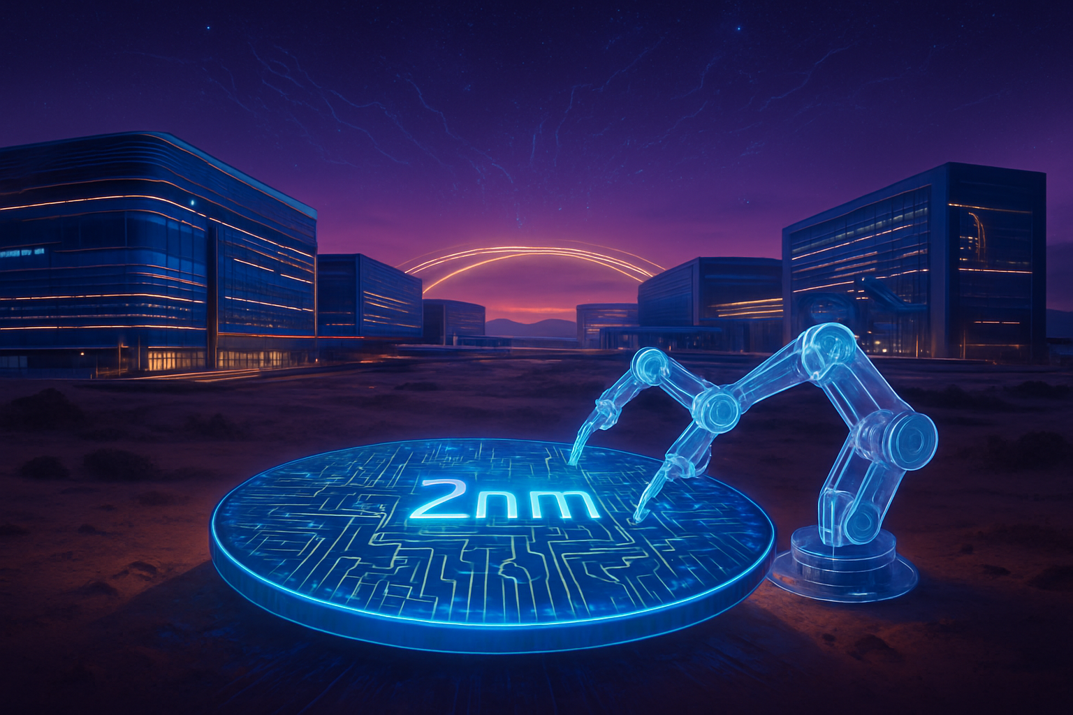
The initial reaction from the AI research community has been cautiously optimistic. Dr. Elena Vance of the AI Policy Institute noted that while the deal may stabilize the prices of "sovereign AI" infrastructure, the administrative burden of managing these complex tariff quotas could create new bottlenecks. Industry experts have praised the move for providing a 10-year roadmap for 2nm and 1.4nm (A16) node production on U.S. soil, which was previously considered a pipe dream by many skeptics of the original 2022 CHIPS Act.
Winners, Losers, and the Battle for Arizona
The implications for major tech players are profound and varied. NVIDIA (NASDAQ: NVDA) stands as a primary beneficiary, with CEO Jensen Huang praising the move as a catalyst for the "AI industrial revolution." By utilizing the TOP, NVIDIA can maintain its margins on its highest-end chips while moving its supply chain into the "safe harbor" of the Phoenix-area data centers. Similarly, Apple (NASDAQ: AAPL) is expected to be the first to utilize the Arizona-made 2nm chips for its 2027 and 2028 device lineups, successfully leveraging its massive scale to secure early capacity in the new facilities.
However, the pact creates a more complex competitive landscape for Intel (NASDAQ: INTC). While Intel benefits from the broader pro-onshoring sentiment, it now faces a direct, localized threat from TSMC’s massive expansion. Analysts at Bernstein have noted that Intel's foundry business must now compete with TSMC on its home turf, not just on technology but also on yield and pricing. Intel CEO Lip-Bu Tan has responded by accelerating the development of the Intel 18A and 14A nodes, emphasizing that "domestic competition" will only sharpen American engineering.
The deal also shifts the strategic position of AMD (NASDAQ: AMD), which has reportedly already begun shifting its logistics toward domestic data center tenants like Riot Platforms (NASDAQ: RIOT) in Texas to bypass potential tariff escalations. For startups in the AI space, the long-term benefit may be more predictable pricing for cloud compute, provided the major providers—Microsoft (NASDAQ: MSFT) and Google (NASDAQ: GOOGL)—can successfully pass through the savings from these tariff exemptions to their customers.
De-risking and the "Silicon Shield" Tension
Beyond the corporate balance sheets, the US-Taiwan deal fits into a broader global trend of "technological balkanization." The imposition of the 25% tariff on non-aligned supply chains is a clear signal that the U.S. is prioritizing national security over the efficiency of the globalized "just-in-time" model. This is a "declaration of economic independence," as described by U.S. officials, aimed at eliminating dependence on East Asian manufacturing hubs that are increasingly vulnerable to geopolitical friction.
However, concerns remain regarding the "Packaging Gap." Experts from Arete Research have pointed out that while wafer fabrication is moving to Arizona, the specialized knowledge for advanced packaging—specifically TSMC's CoWoS (Chip on Wafer on Substrate) technology—remains concentrated in Taiwan. Without a full "end-to-end" ecosystem in the U.S., the supply chain remains a "Silicon Bridge" rather than a self-contained island. If wafers still have to be shipped back to Asia for final packaging, the geopolitical de-risking remains incomplete.
Furthermore, there is a palpable sense of irony in Taipei. For decades, Taiwan’s dominant position in the chip world—its "Silicon Shield"—has been its ultimate insurance policy. If the U.S. achieves 20% of the world’s most advanced logic production, some fear that Washington’s incentive to defend the island could diminish. This tension was likely a key driver behind the Taiwanese government's demand for $250 billion in credit guarantees as part of the deal, ensuring that the move to the U.S. is as much about mutual survival as it is about business.
The Road to 1.4nm: What’s Next for Arizona?
Looking ahead, the next 24 to 36 months will be critical for the execution of this deal. The first Arizona fab is already in volume production using the N4 process, but the true test will be the structural completion of the second and third fabs, which are targeted for N3 and N2 nodes by late 2027. We can expect to see a surge in specialized labor recruitment, as the 11-fab plan will require an estimated 30,000 highly skilled engineers and technicians—a workforce that the U.S. currently lacks.
Potential applications on the horizon include the first generation of "fully domestic" AI supercomputers, which will be exempt from the 25% tariff and could serve as the foundation for the next wave of military and scientific breakthroughs. We are also likely to see a flurry of announcements from chemical and material suppliers like ASML (NASDAQ: ASML) and Applied Materials (NASDAQ: AMAT), as they build out their own service hubs in the Phoenix and Austin regions to support the new capacity.
The challenges, however, are not just technical. Addressing the high cost of construction and energy in the U.S. will be paramount. If the "per-wafer" cost of an Arizona-made 2nm chip remains significantly higher than its Taiwanese counterpart, the U.S. government may be forced to extend these "temporary" tariffs and offsets indefinitely, creating a permanent, bifurcated market for semiconductors.
A New Era for the Digital Age
The January 2026 US-Taiwan semiconductor deal marks a turning point in AI history. It is the moment where the "invisible hand" of the market was replaced by the "visible hand" of industrial policy. By trading market access for physical infrastructure, the U.S. and Taiwan have fundamentally altered the path of the digital age, prioritizing resilience and national security over the cost-savings of the past three decades.
The key takeaways from this landmark agreement are clear: the U.S. is committed to becoming a global center for advanced logic manufacturing, Taiwan remains an indispensable partner but one whose role is evolving, and the AI industry is now officially a matter of statecraft. In the coming months, the industry will be watching for the first "TOP-certified" imports and the progress of the Arizona groundbreaking ceremonies. While the "Silicon Bridge" is now under construction, its durability will depend on whether the U.S. can truly foster the deep, complex ecosystem required to sustain the world’s most advanced technology on its own soil.
This content is intended for informational purposes only and represents analysis of current AI developments.
TokenRing AI delivers enterprise-grade solutions for multi-agent AI workflow orchestration, AI-powered development tools, and seamless remote collaboration platforms.
For more information, visit https://www.tokenring.ai/.