Category: Uncategorized

  • Samsung’s 800 Million Device Moonshot: The AI Ecosystem Revolution Led by Gemini 3 and Perplexity

    Samsung’s 800 Million Device Moonshot: The AI Ecosystem Revolution Led by Gemini 3 and Perplexity

    In a bold move to dominate the next era of personal computing, Samsung Electronics Co., Ltd. (KRX: 005930) has officially announced an ambitious roadmap to bring its "Galaxy AI" suite to 800 million devices by the end of 2026. This target, revealed by co-CEO T.M. Roh in early January 2026, represents a massive doubling of the company’s 2025 goals and signals a shift from AI as a premium smartphone feature to a ubiquitous "ambient layer" across the world’s largest consumer electronics ecosystem.

    The announcement marks a pivotal moment for the industry, as Samsung moves beyond simple chatbots to integrate sophisticated, multi-modal intelligence into everything from the upcoming Galaxy S26 flagship to smart refrigerators and Micro LED televisions. By leveraging deep-tier partnerships with Alphabet Inc. (NASDAQ: GOOGL) and the rising search giant Perplexity AI, Samsung is positioning itself as the primary gatekeeper for consumer AI, aiming to outpace competitors through sheer scale and cross-device synergy.

    The Technical Backbone: Gemini 3 and the Rebirth of Bixby

    At the heart of Samsung’s 2026 expansion is the integration of Google’s recently released Gemini 3 model. Unlike its predecessors, Gemini 3 offers significantly enhanced on-device processing capabilities, allowing Galaxy devices to handle complex multi-modal tasks—such as real-time video analysis and sophisticated reasoning—without constantly relying on the cloud. This integration powers the new "Bixby Live" feature in One UI 8.5, which introduces eight specialized AI agents capable of everything from acting as a real-time "Storyteller" for children to a "Dress Matching" fashion consultant that uses the device's camera to analyze a user's wardrobe.

    The partnership with Perplexity AI addresses one of Bixby’s long-standing hurdles: the "hallucination" and limited knowledge of traditional voice assistants. By integrating Perplexity’s real-time search engine, Bixby can now function as a professional researcher, providing cited, up-to-the-minute answers to complex queries. Furthermore, the 2026 appliance lineup, including the Bespoke AI Refrigerator Family Hub, utilizes Gemini 3-powered AI Vision to recognize over 1,500 food items, automatically tracking expiration dates and suggesting recipes. This is a significant leap from the 2024 models, which were limited to basic image recognition for a few dozen items.

    A New Power Dynamic in the AI Arms Race

    Samsung’s aggressive 800-million-device goal creates a formidable challenge for Apple Inc. (NASDAQ: AAPL), whose "Apple Intelligence" has remained largely focused on the iPhone and Mac ecosystems. By embedding high-end AI into mid-range A-series phones and home appliances, Samsung is effectively "democratizing" advanced AI, forcing competitors to either lower their hardware requirements or risk losing market share in the burgeoning smart home sector. Google also stands as a primary beneficiary; through Samsung, Gemini 3 gains a massive hardware distribution channel that rivals the reach of Microsoft (NASDAQ: MSFT) and its Windows Copilot integration.

    For Perplexity, the partnership is a strategic masterstroke, granting the startup immediate access to hundreds of millions of users and positioning it as a viable alternative to traditional search. This collaboration disrupts the existing search paradigm, as users increasingly turn to their voice assistants for cited information rather than clicking through blue links on a browser. Industry experts suggest that if Samsung successfully hits its 2026 target, it will control the most diverse data set in the AI industry, spanning mobile usage, home habits, and media consumption.

    Ambient Intelligence and the Privacy Frontier

    The shift toward "Ambient AI"—where intelligence is integrated into the physical environment through TVs and appliances—marks a departure from the "screen-first" era of the last decade. Samsung’s use of Voice ID technology allows its 2026 appliances to recognize individual family members by their vocal prints, delivering personalized schedules and health data. While this offers unprecedented convenience, it also raises significant concerns regarding data privacy and the "always-listening" nature of 800 million connected microphones.

    Samsung has attempted to mitigate these concerns by emphasizing its "Knox Matrix" security, which uses blockchain-based encryption to keep sensitive AI processing on-device or within a private home network. However, as AI becomes an invisible layer of daily life, the industry is watching closely to see how Samsung balances its massive data harvesting needs with the increasing global demand for digital sovereignty. This milestone echoes the early days of the smartphone revolution, but with the stakes raised by the predictive and autonomous nature of generative AI.

    The Road to 2027: What Lies Ahead

    Looking toward the latter half of 2026, the launch of the Galaxy S26 and the rumored "Galaxy Z TriFold" will be the true litmus tests for Samsung’s AI ambitions. These devices are expected to debut with "Hey Plex" as a native wake-word option, further blurring the lines between hardware and AI services. Experts predict that the next frontier for Samsung will be "Autonomous Task Orchestration," where Bixby doesn't just answer questions but executes multi-step workflows across devices—such as ordering groceries when the fridge is low and scheduling a delivery time that fits the user’s calendar.

    The primary challenge remains the "utility gap"—ensuring that these 800 million devices provide meaningful value rather than just novelty features. As the AI research community moves toward "Agentic AI," Samsung’s hardware variety provides a unique laboratory for testing how AI can assist in physical tasks. If the company can maintain its current momentum, the end of 2026 could mark the year that artificial intelligence officially moved from our pockets into the very fabric of our homes.

    Final Thoughts: A Defining Moment for Samsung

    Samsung’s 800 million device goal is more than just a sales target; it is a declaration of intent to define the AI era. By combining the software prowess of Google and Perplexity with its own unparalleled hardware manufacturing scale, Samsung is building a moat that few can cross. The integration of Gemini 3 and the transformation of Bixby represent a total reimagining of the user interface, moving us closer to a world where technology anticipates our needs without being asked.

    As we move through 2026, the tech world will be watching the adoption rates of One UI 8.5 and the performance of the new Bespoke AI appliances. The success of this "Moonshot" will likely determine the hierarchy of the tech industry for the next decade. For now, Samsung has laid down a gauntlet that demands a response from every major player in Silicon Valley and beyond.


    This content is intended for informational purposes only and represents analysis of current AI developments.

    TokenRing AI delivers enterprise-grade solutions for multi-agent AI workflow orchestration, AI-powered development tools, and seamless remote collaboration platforms.
    For more information, visit https://www.tokenring.ai/.

  • Google Redefines the Inbox: Gemini 3 Integration Turns Gmail into a Proactive Personal Assistant

    Google Redefines the Inbox: Gemini 3 Integration Turns Gmail into a Proactive Personal Assistant

    In a move that signals the most profound shift in personal productivity since the dawn of the cloud era, Alphabet Inc. (NASDAQ: GOOGL) has officially integrated its next-generation Gemini 3 model into Gmail. Announced this week, the update transforms Gmail from a static repository of messages into a proactive "AI Inbox" capable of managing a user’s digital life. By leveraging the reasoning capabilities of Gemini 3, Google aims to eliminate the "inbox fatigue" that has plagued users for decades, repositioning email as a structured command center rather than a chaotic list of unread notifications.

    The significance of this deployment lies in its scale and sophistication. With over three billion users, Google is effectively conducting the world’s largest rollout of agentic AI. The update introduces a dedicated "AI Inbox" view that clusters emails by topic and extracts actionable "Suggested To-Dos," alongside a conversational natural language search that allows users to query their entire communication history as if they were speaking to a human archivist. As the "Gemini Era" takes hold, the traditional chronological inbox is increasingly becoming a secondary feature to the AI-curated experience.

    Technical Evolution: The "Thinking" Model Architecture

    At the heart of this transformation is Gemini 3, a model Google describes as its first true "thinking" engine. Unlike its predecessors, which focused primarily on pattern recognition and speed, Gemini 3 introduces a "Dynamic Thinking" layer. This allows the model to modulate its reasoning time based on the complexity of the task; a simple draft might be generated instantly, while a request to "summarize all project expenses from the last six months" triggers a deeper reasoning process. Technical benchmarks indicate that Gemini 3 Pro outperforms previous iterations significantly, particularly in logical reasoning and visual data parsing, while operating roughly 3x faster than the Gemini 2.0 Pro model.

    The "AI Inbox" utilizes this reasoning to perform semantic clustering. Rather than just grouping emails by sender or subject line, Gemini 3 understands the context of conversations—distinguishing, for example, between a "travel" thread that requires immediate action (like a check-in) and one that is merely informational. The new Natural Language Search is equally transformative; it replaces keyword-matching with a retrieval-augmented generation (RAG) system. Users can ask, "What were the specific terms of the bathroom renovation quote I received last autumn?" and receive a synthesized answer with citations to specific threads, even if the word "quote" was never explicitly used in the subject line.

    This architectural shift also addresses efficiency. Google reports that Gemini 3 uses 30% fewer tokens to complete complex tasks compared to earlier versions, a critical optimization for maintaining a fluid mobile experience. For users, this means the "Help Me Write" tool—now free for all users—can draft context-aware replies that mimic the user's personal tone and style with startling accuracy. The model no longer just predicts the next word; it predicts the intent of the communication, offering suggested replies that can handle multi-step tasks, such as proposing a meeting time by cross-referencing the user's Google Calendar.

    Market Dynamics: A Strategic Counter to Microsoft and Apple

    The integration of Gemini 3 is a clear shot across the bow of Microsoft (NASDAQ: MSFT) and its Copilot ecosystem. By making the core "Help Me Write" features free for its entire user base, Google is aggressively democratizing AI productivity to maintain its dominance in the consumer space. While Microsoft has found success in the enterprise sector with its 365 Copilot, Google’s move to provide advanced AI tools to three billion people creates a massive data and feedback loop that could accelerate its lead in consumer-facing generative AI.

    This development has immediate implications for the competitive landscape. Alphabet’s stock hit record highs following the announcement, as investors bet on the company's ability to monetize its AI lead through tiered subscriptions. The new "Google AI Ultra" tier, priced at $249.99/month for enterprise power users, introduces a "Deep Think" mode for high-stakes reasoning, directly competing with specialized AI labs and high-end productivity startups. Meanwhile, Apple (NASDAQ: AAPL) remains under pressure to show that its own "Apple Intelligence" can match the cross-app reasoning and deep integration now present in the Google Workspace ecosystem.

    For the broader startup ecosystem, Google’s "AI Inbox" may pose an existential threat to niche "AI-first" email clients. Startups that built their value proposition on summarizing emails or providing better search now find their core features integrated natively into the world’s most popular email platform. To survive, these smaller players will likely need to pivot toward hyper-specialized workflows or provide "sovereign AI" solutions for users who remain wary of big-tech data aggregation.

    The Broader AI Landscape: Privacy, Utility, and Hallucination

    The rollout of Gemini 3 into Gmail marks a milestone in the "agentic" trend of artificial intelligence, where models move from being chatbots to active participants in digital workflows. This transition is not without its concerns. Privacy remains the primary hurdle for widespread adoption. Google has gone to great lengths to emphasize that Gmail data is not used to train its public models and is protected by "engineering privacy" barriers, yet the prospect of an AI "reading" every email to suggest to-dos will inevitably trigger regulatory scrutiny, particularly in the European Union.

    Furthermore, the issue of AI "hallucination" takes on new weight when applied to an inbox. If an AI incorrectly summarizes a bill's due date or misses a critical nuance in a legal thread, the consequences are more tangible than a wrong answer in a chat interface. Google’s "AI Inbox" attempts to mitigate this by providing direct citations and links to the original emails for every summary it generates, encouraging a "trust but verify" relationship between the user and the assistant.

    This integration also reflects a broader shift in how humans interact with information. We are moving away from the "search and browse" era toward a "query and synthesize" era. As users grow accustomed to asking their inbox questions rather than scrolling through folders, the very nature of digital literacy will change. The success of Gemini 3 in Gmail will likely serve as a blueprint for how AI will eventually be integrated into other high-friction digital environments, such as file management and project coordination.

    The Road Ahead: Autonomous Agents and Predictive Actions

    Looking forward, the Gemini 3 integration is merely the foundation for what experts call "Autonomous Inbox Management." In the near term, we can expect Google to expand the "AI Inbox" to include predictive actions—where the AI doesn't just suggest a to-do, but offers to complete it. This could involve automatically paying a recurring bill or rescheduling a flight based on a cancellation email, provided the user has granted the necessary permissions.

    The long-term challenge for Google will be the "agent-to-agent" economy. As more users employ AI assistants to write and manage their emails, we may reach a point where the majority of digital communication is conducted between AI models rather than humans. This raises fascinating questions about the future of language and social norms. If an AI writes an email and another AI summarizes it, does the original nuance of the human sender still matter? Addressing these philosophical and technical challenges will be the next frontier for the Gemini team.

    Summary of the Gemini 3 Revolution

    The integration of Gemini 3 into Gmail represents a pivotal moment in the history of artificial intelligence. By turning the world’s most popular email service into a proactive assistant, Google has moved beyond the "chatbot" phase of AI and into the era of integrated, agentic utility. The tiered access model ensures that while the masses benefit from basic productivity gains, power users and enterprises have access to a high-reasoning engine that can navigate the complexities of modern professional life.

    As we move through 2026, the tech industry will be watching closely to see how these tools impact user behavior and whether the promised productivity gains actually materialize. For now, the "AI Inbox" stands as a testament to the rapid pace of AI development and a glimpse into a future where our digital tools don't just store our information, but actively help us manage our lives.


    This content is intended for informational purposes only and represents analysis of current AI developments.

    TokenRing AI delivers enterprise-grade solutions for multi-agent AI workflow orchestration, AI-powered development tools, and seamless remote collaboration platforms.
    For more information, visit https://www.tokenring.ai/.

  • Meta’s Nuclear Gambit: A 6.6-Gigawatt Leap to Power the Age of ‘Prometheus’

    Meta’s Nuclear Gambit: A 6.6-Gigawatt Leap to Power the Age of ‘Prometheus’

    In a move that fundamentally reshapes the intersection of big tech and the global energy sector, Meta Platforms Inc. (NASDAQ:META) has announced a staggering 6.6-gigawatt (GW) nuclear power procurement strategy. This unprecedented commitment, unveiled on January 9, 2026, represents the largest corporate investment in nuclear energy to date, aimed at securing a 24/7 carbon-free power supply for the company’s next generation of artificial intelligence "superclusters." By partnering with industry giants and innovators, Meta is positioning itself to overcome the primary bottleneck of the AI era: the massive, unyielding demand for electrical power.

    The significance of this announcement cannot be overstated. As the race toward Artificial Superintelligence (ASI) intensifies, the availability of "firm" baseload power—energy that does not fluctuate with the weather—has become the ultimate competitive advantage. Meta’s multi-pronged agreement with Vistra Corp. (NYSE:VST), Oklo Inc. (NYSE:OKLO), and the Bill Gates-backed TerraPower ensures that its "Prometheus" and "Hyperion" data centers will have the necessary fuel to train models of unimaginable scale, while simultaneously revitalizing the American nuclear supply chain.

    The 6.6 GW portfolio is a sophisticated blend of existing infrastructure and frontier technology. At the heart of the agreement is a massive commitment to Vistra Corp., which will provide over 2.1 GW of power through 20-year Power Purchase Agreements (PPAs) from the Perry, Davis-Besse, and Beaver Valley plants. This deal includes funding for 433 megawatts (MW) of "uprates"—technical modifications to existing reactors that increase their efficiency and output. This approach provides Meta with immediate, reliable power while extending the operational life of critical American energy assets into the mid-2040s.

    Beyond traditional nuclear, Meta is placing a significant bet on the future of Small Modular Reactors (SMRs) and advanced reactor designs. The partnership with Oklo Inc. involves a 1.2 GW "power campus" in Pike County, Ohio, utilizing Oklo’s Aurora powerhouse technology. These SMRs are designed to operate on recycled nuclear fuel, offering a more sustainable and compact alternative to traditional light-water reactors. Simultaneously, Meta’s deal with TerraPower focuses on "Natrium" technology—a sodium-fast reactor that uses liquid sodium as a coolant. Unlike water-cooled systems, Natrium reactors operate at higher temperatures and include integrated molten salt energy storage, allowing the facility to boost its power output for hours at a time to meet peak AI training demands.

    These energy assets are directly tied to Meta’s most ambitious infrastructure projects: the Prometheus and Hyperion data centers. Prometheus, a 1 GW AI supercluster in New Albany, Ohio, is scheduled to come online later this year and will serve as the primary testing ground for Meta’s most advanced generative models. Hyperion, an even more massive 5 GW facility in rural Louisiana, represents a $27 billion investment designed to house the hardware required for the next decade of AI breakthroughs. While Hyperion will initially utilize natural gas to meet its immediate 2028 operational goals, the 6.6 GW nuclear portfolio is designed to transition Meta’s entire AI fleet to carbon-neutral power by 2035.

    Meta’s nuclear surge sends a clear signal to its primary rivals: Microsoft (NASDAQ:MSFT), Google (NASDAQ:GOOGL), and Amazon (NASDAQ:AMZN). While Microsoft previously set the stage with its deal to restart a reactor at Three Mile Island, Meta’s 6.6 GW commitment is nearly eight times larger in scale. By securing such a massive portion of the available nuclear capacity in the PJM Interconnection region—the energy heartland of American data centers—Meta is effectively "moating" its energy supply, making it more difficult for competitors to find the firm power needed for their own mega-projects.

    Industry analysts suggest that this move provides Meta with a significant strategic advantage in the race for AGI. As AI models grow exponentially in complexity, the cost of electricity is becoming a dominant factor in the total cost of ownership for AI systems. By locking in long-term, fixed-rate contracts for nuclear power, Meta is insulating itself from the volatility of natural gas prices and the rising costs of grid congestion. Furthermore, the partnership with Oklo and TerraPower allows Meta to influence the design and deployment of energy tech specifically tailored for high-compute environments, potentially creating a proprietary blueprint for AI-integrated energy infrastructure.

    The broader significance of this deal extends far beyond Meta’s balance sheet. It marks a pivotal moment in the "AI-Nuclear" nexus, where the demands of the tech industry act as the primary catalyst for a nuclear renaissance in the United States. For decades, the American nuclear industry has struggled with high capital costs and long construction timelines. By acting as a foundational "off-taker" for 6.6 GW of power, Meta is providing the financial certainty required for companies like Oklo and TerraPower to move from prototypes to commercial-scale deployment.

    This development is also a cornerstone of American energy policy and national security. Meta Policy Chief Joel Kaplan has noted that these agreements are essential for "securing the U.S.'s position as the global leader in AI innovation." By subsidizing the de-risking of next-generation American nuclear technology, Meta is helping to build a domestic supply chain that can compete with state-sponsored energy initiatives in China and Russia. However, the plan is not without its critics; environmental groups and local communities have expressed concerns regarding the speed of SMR deployment and the long-term management of nuclear waste, even as Meta promises to pay the "full costs" of infrastructure to avoid burdening residential taxpayers.

    While the 6.6 GW announcement is a historic milestone, the path to 2035 is fraught with challenges. The primary hurdle remains the Nuclear Regulatory Commission (NRC), which must approve the novel designs of the Oklo and TerraPower reactors. While the NRC has signaled a willingness to streamline the licensing process for advanced reactors, the timeline for "first-of-a-kind" technology is notoriously unpredictable. Meta and its partners will need to navigate a complex web of safety evaluations, environmental reviews, and public hearings to stay on schedule.

    In the near term, the focus will shift to the successful completion of the Vistra uprates and the initial construction phases of the Prometheus data center. Experts predict that if Meta can successfully integrate nuclear power into its AI operations at this scale, it will set a new global standard for "green" AI. We may soon see a trend where data center locations are chosen not based on proximity to fiber optics, but on proximity to dedicated nuclear "power campuses." The ultimate goal remains the realization of Artificial Superintelligence, and with 6.6 GW of power on the horizon, the electrical constraints that once seemed insurmountable are beginning to fade.

    Meta’s 6.6 GW nuclear agreement is more than just a utility contract; it is a declaration of intent. By securing a massive, diversified portfolio of traditional and advanced nuclear energy, Meta is ensuring that its AI ambitions—embodied by the Prometheus and Hyperion superclusters—will not be sidelined by a crumbling or carbon-heavy electrical grid. The deal provides a lifeline to the American nuclear industry, signals a new phase of competition among tech giants, and reinforces the United States' role as the epicenter of the AI revolution.

    As we move through 2026, the industry will be watching closely for the first signs of construction at the Oklo campus in Ohio and the regulatory milestones of TerraPower’s Natrium reactors. This development marks a definitive chapter in AI history, where the quest for digital intelligence has become the most powerful driver of physical energy innovation. The long-term impact of this "Nuclear Gambit" may well determine which company—and which nation—crosses the finish line in the race for the next era of computing.


    This content is intended for informational purposes only and represents analysis of current AI developments.

    TokenRing AI delivers enterprise-grade solutions for multi-agent AI workflow orchestration, AI-powered development tools, and seamless remote collaboration platforms.
    For more information, visit https://www.tokenring.ai/.

  • NVIDIA Unveils Vera Rubin AI Platform at CES 2026: A 5x Performance Leap into the Era of Agentic AI

    NVIDIA Unveils Vera Rubin AI Platform at CES 2026: A 5x Performance Leap into the Era of Agentic AI

    In a landmark keynote at the 2026 Consumer Electronics Show (CES) in Las Vegas, NVIDIA (NASDAQ: NVDA) CEO Jensen Huang officially introduced the Vera Rubin AI platform, the successor to the company’s highly successful Blackwell architecture. Named after the pioneering astronomer who provided the first evidence for dark matter, the Rubin platform is designed to power the next generation of "agentic AI"—autonomous systems capable of complex reasoning and long-term planning. The announcement marks a pivotal shift in the AI infrastructure landscape, promising a staggering 5x performance increase over Blackwell and a radical departure from traditional data center cooling methods.

    The immediate significance of the Vera Rubin platform lies in its ability to dramatically lower the cost of intelligence. With a 10x reduction in the cost of generating inference tokens, NVIDIA is positioning itself to make massive-scale AI models not only more capable but also commercially viable for a wider range of industries. As the industry moves toward "AI Superfactories," the Rubin platform serves as the foundational blueprint for the next decade of accelerated computing, integrating compute, networking, and cooling into a single, cohesive ecosystem.

    Engineering the Future: The 6-Chip Architecture and Liquid-Cooled Dominance

    The technical heart of the Vera Rubin platform is an "extreme co-design" philosophy that integrates six distinct, high-performance chips. At the center is the NVIDIA Rubin GPU, a dual-die powerhouse fabricated on TSMC’s (NYSE: TSM) 3nm process, boasting 336 billion transistors. It is the first GPU to utilize HBM4 memory, delivering up to 22 TB/s of bandwidth—a 2.8x improvement over Blackwell. Complementing the GPU is the NVIDIA Vera CPU, built with 88 custom "Olympus" ARM (NASDAQ: ARM) cores. This CPU offers 2x the performance and bandwidth of the previous Grace CPU, featuring 1.8 TB/s NVLink-C2C connectivity to ensure seamless data movement between the processor and the accelerator.

    Rounding out the 6-chip architecture are the BlueField-4 DPU, the NVLink 6 Switch, the ConnectX-9 SuperNIC, and the Spectrum-6 Ethernet Switch. The BlueField-4 DPU is a massive upgrade, featuring a 64-core CPU and an integrated 800 Gbps SuperNIC designed to accelerate agentic reasoning. Perhaps most impressive is the NVLink 6 Switch, which provides 3.6 TB/s of bidirectional bandwidth per GPU, enabling a rack-scale bandwidth of 260 TB/s—exceeding the total bandwidth of the global internet. This level of integration allows the Rubin platform to deliver 50 PFLOPS of NVFP4 compute for AI inference, a 5-fold leap over the Blackwell B200.

    Beyond raw compute, NVIDIA has reinvented the physical form factor of the data center. The flagship Vera Rubin NVL72 system is 100% liquid-cooled and features a "fanless" compute tray design. By removing mechanical fans and moving to warm-water Direct Liquid Cooling (DLC), NVIDIA has eliminated one of the primary points of failure in high-density environments. This transition allows for rack power densities exceeding 130 kW, nearly double that of previous generations. Industry experts have noted that this "silent" architecture is not just an engineering feat but a necessity, as the power requirements for next-gen AI training have finally outpaced the capabilities of traditional air cooling.

    Market Dominance and the Cloud Titan Alliance

    The launch of Vera Rubin has immediate and profound implications for the world’s largest technology companies. NVIDIA announced that the platform is already in full production, with major cloud service providers set to begin deployments in the second half of 2026. Microsoft (NASDAQ: MSFT) has committed to deploying Rubin in its upcoming "Fairwater AI Superfactories," which are expected to power the next generation of models from OpenAI. Similarly, Amazon (NASDAQ: AMZN) Web Services (AWS) and Alphabet (NASDAQ: GOOGL) through Google Cloud have signed on as early adopters, ensuring that the Rubin architecture will be the backbone of the global AI cloud by the end of the year.

    For competitors like AMD (NASDAQ: AMD) and Intel (NASDAQ: INTC), the Rubin announcement sets an incredibly high bar. The 5x performance leap and the integration of HBM4 memory put NVIDIA several steps ahead in the "arms race" for AI hardware. Furthermore, by providing a full-stack solution—from the CPU and GPU to the networking switches and liquid-cooling manifolds—NVIDIA is making it increasingly difficult for customers to mix and match components from other vendors. This "lock-in" is bolstered by the Rubin MGX architecture, which hardware partners like Super Micro Computer (NASDAQ: SMCI), Dell Technologies (NYSE: DELL), Hewlett Packard Enterprise (NYSE: HPE), and Lenovo (HKEX: 0992) are already using to build standardized rack-scale solutions.

    Strategic advantages also extend to specialized AI labs and startups. The 10x reduction in token costs means that startups can now run sophisticated agentic workflows that were previously cost-prohibitive. This could lead to a surge in "AI-native" applications that require constant, high-speed reasoning. Meanwhile, established giants like Oracle (NYSE: ORCL) are leveraging Rubin to offer sovereign AI clouds, allowing nations to build their own domestic AI capabilities using NVIDIA's high-efficiency, liquid-cooled infrastructure.

    The Broader AI Landscape: Sustainability and the Pursuit of AGI

    The Vera Rubin platform arrives at a time when the environmental impact of AI is under intense scrutiny. The shift to a 100% liquid-cooled, fanless design is a direct response to concerns regarding the massive energy consumption of data centers. By delivering 8x better performance-per-watt for inference tasks compared to Blackwell, NVIDIA is attempting to decouple AI progress from exponential increases in power demand. This focus on sustainability is likely to become a key differentiator as global regulations on data center efficiency tighten throughout 2026.

    In the broader context of AI history, the Rubin platform represents the transition from "Generative AI" to "Agentic AI." While Blackwell was optimized for large language models that generate text and images, Rubin is designed for models that can interact with the world, use tools, and perform multi-step reasoning. This architectural shift mirrors the industry's pursuit of Artificial General Intelligence (AGI). The inclusion of "Inference Context Memory Storage" in the BlueField-4 DPU specifically targets the long-context requirements of these autonomous agents, allowing them to maintain "memory" over much longer interactions than was previously possible.

    However, the rapid pace of development also raises concerns. The sheer scale of the Rubin NVL72 racks—and the infrastructure required to support 130 kW densities—means that only the most well-capitalized organizations can afford to play at the cutting edge. This could further centralize AI power among a few "hyper-scalers" and well-funded nations. Comparisons are already being made to the early days of the space race, where the massive capital requirements for infrastructure created a high barrier to entry that only a few could overcome.

    Looking Ahead: The H2 2026 Rollout and Beyond

    As we look toward the second half of 2026, the focus will shift from announcement to implementation. The rollout of Vera Rubin will be the ultimate test of the global supply chain's ability to handle high-precision liquid-cooling components and 3nm chip production at scale. Experts predict that the first Rubin-powered models will likely emerge in late 2026, potentially featuring trillion-parameter architectures that can process multi-modal data in real-time with near-zero latency.

    One of the most anticipated applications for the Rubin platform is in the field of "Physical AI"—the integration of AI agents into robotics and autonomous manufacturing. The high-bandwidth, low-latency interconnects of the Rubin architecture are ideally suited for the massive sensor-fusion tasks required for humanoid robots to navigate complex environments. Additionally, the move toward "Sovereign AI" is expected to accelerate, with more countries investing in Rubin-based clusters to ensure their economic and national security in an increasingly AI-driven world.

    Challenges remain, particularly in the realm of software. While the hardware offers a 5x performance leap, the software ecosystem (CUDA and beyond) must evolve to fully utilize the asynchronous processing capabilities of the 6-chip architecture. Developers will need to rethink how they distribute workloads across the Vera CPU and Rubin GPU to avoid bottlenecks. What happens next will depend on how quickly the research community can adapt their models to this new "extreme co-design" paradigm.

    Conclusion: A New Era of Accelerated Computing

    The launch of the Vera Rubin platform at CES 2026 is more than just a hardware refresh; it is a fundamental reimagining of what a computer is. By integrating compute, networking, and thermal management into a single, fanless, liquid-cooled system, NVIDIA has set a new standard for the industry. The 5x performance increase and 10x reduction in token costs provide the economic fuel necessary for the next wave of AI innovation, moving us closer to a world where autonomous agents are an integral part of daily life.

    As we move through 2026, the industry will be watching the H2 deployment closely. The success of the Rubin platform will be measured not just by its benchmarks, but by its ability to enable breakthroughs in science, healthcare, and sustainability. For now, NVIDIA has once again proven its ability to stay ahead of the curve, delivering a platform that is as much a work of art as it is a feat of engineering. The "Rubin Revolution" has officially begun, and the AI landscape will never be the same.


    This content is intended for informational purposes only and represents analysis of current AI developments.

    TokenRing AI delivers enterprise-grade solutions for multi-agent AI workflow orchestration, AI-powered development tools, and seamless remote collaboration platforms.
    For more information, visit https://www.tokenring.ai/.
  • Silicon-Level Fortresses: How 2026’s Next-Gen Chips are Locking Down Trillion-Dollar AI Models

    Silicon-Level Fortresses: How 2026’s Next-Gen Chips are Locking Down Trillion-Dollar AI Models

    The artificial intelligence revolution has reached a critical inflection point where the value of model weights—the "secret sauce" of LLMs—now represents trillions of dollars in research and development. As of January 9, 2026, the industry has shifted its focus from mere performance to "Confidential Computing," a hardware-first security paradigm that ensures sensitive data and proprietary AI models remain encrypted even while they are being processed. This breakthrough effectively turns silicon into a fortress, allowing enterprises to deploy their most valuable intellectual property in public clouds without the risk of exposure to cloud providers, hackers, or even state-sponsored actors.

    The emergence of these hardware-level protections marks the end of the "trust but verify" era in cloud computing. With the release of next-generation architectures from industry leaders, the "black box" of AI inference has become a literal secure vault. By isolating AI workloads within hardware-based Trusted Execution Environments (TEEs), companies can now run frontier models like GPT-5 and Llama 4 with the mathematical certainty that their weights cannot be scraped or leaked from memory, even if the underlying operating system is compromised.

    The Architecture of Trust: Rubin, MI400, and the Rise of TEEs

    At the heart of this security revolution is NVIDIA’s (NASDAQ:NVDA) newly launched Vera Rubin platform. Succeeding the Blackwell architecture, the Rubin NVL72 introduces the industry’s first rack-scale Trusted Execution Environment. Unlike previous generations that secured individual chips, the Rubin architecture extends protection across the entire NVLink domain. This is critical for 2026’s trillion-parameter models, which are too large for a single GPU and must be distributed across dozens of chips. Through the BlueField-4 Data Processing Unit (DPU) and the Advanced Secure Trusted Resource Architecture (ASTRA), NVIDIA provides hardware-accelerated attestation, ensuring that model weights are only decrypted within the secure memory space of the Rubin GPU.

    AMD (NASDAQ:AMD) has countered with its Instinct MI400 series and the Helios platform, positioning itself as the primary choice for "Sovereign AI." Built on the CDNA 5 architecture, the MI400 leverages AMD’s SEV-SNP (Secure Encrypted Virtualization-Secure Nested Paging) technology to provide rigorous memory isolation. The MI400 features up to 432GB of HBM4 memory, where every byte is encrypted at the controller level. This prevents "cold boot" attacks and memory scraping, which were theoretical vulnerabilities in earlier AI hardware. AMD’s Helios rack-scale security pairs these GPUs with EPYC "Venice" CPUs, which act as a hardware root of trust to verify the integrity of the entire software stack before any processing begins.

    Intel (NASDAQ:INTC) has also redefined its roadmap with the introduction of Jaguar Shores, a next-generation AI accelerator designed specifically for secure enterprise inference. Jaguar Shores utilizes Intel’s Trust Domain Extensions (TDX) and a new feature called TDX Connect. This technology provides a secure, encrypted PCIe/CXL 3.1 link between the Xeon processor and the accelerator, ensuring that data moving between the CPU and GPU is never visible to the system bus in plaintext. This differs significantly from previous approaches that relied on software-level encryption, which added massive latency and was susceptible to side-channel attacks. Initial reactions from the research community suggest that these hardware improvements have finally closed the "memory gap" that previously left AI models vulnerable during high-speed computation.

    Strategic Shifts: The New Competitive Landscape for Tech Giants

    This shift toward hardware-level security is fundamentally altering the competitive dynamics of the cloud and semiconductor industries. Cloud giants like Microsoft (NASDAQ:MSFT), Amazon (NASDAQ:AMZN), and Alphabet (NASDAQ:GOOGL) are no longer just selling compute cycles; they are selling "zero-trust" environments. Microsoft’s Azure AI Foundry now offers Confidential VMs powered by NVIDIA Rubin GPUs, allowing customers to deploy proprietary models with "Application Inference Profiles" that prevent model scraping. This has become a major selling point for financial institutions and healthcare providers who were previously hesitant to move their most sensitive AI workloads to the public cloud.

    For semiconductor companies, security has become as important a metric as TeraFLOPS. NVIDIA’s integration of ASTRA across its rack-scale systems gives it a strategic advantage in the enterprise market, where the loss of a proprietary model could bankrupt a company. However, AMD’s focus on open-standard security through the UALink (Ultra Accelerator Link) and its Helios architecture is gaining traction among governments and "Sovereign AI" initiatives that are wary of proprietary, locked-down ecosystems. This competition is driving a rapid standardization of attestation protocols, making it easier for startups to switch between hardware providers while maintaining a consistent security posture.

    The disruption is also hitting the AI model-as-a-service (MaaS) market. As hardware-level security becomes ubiquitous, the barrier to "bringing your own model" (BYOM) to the cloud has vanished. Startups that once relied on providing API access to their models are now facing pressure to allow customers to run those models in their own confidential cloud enclaves. This shifts the value proposition from simple access to the integrity and privacy of the execution environment, forcing AI labs to rethink how they monetize and distribute their intellectual property.

    Global Implications: Sovereignty, Privacy, and the New Regulatory Era

    The broader significance of hardware-level AI security extends far beyond corporate balance sheets; it is becoming a cornerstone of national security and regulatory compliance. With the EU AI Act and other global frameworks now in full effect as of 2026, the ability to prove that data remains private during inference is a legal requirement for many industries. Confidential computing provides a technical solution to these regulatory demands, allowing for "Privacy-Preserving Machine Learning" where multiple parties can train a single model on a shared dataset without any party ever seeing the others' raw data.

    This development also plays a crucial role in the concept of AI Sovereignty. Nations are increasingly concerned about their citizens' data being processed on foreign-controlled hardware. By utilizing hardware-level TEEs and local attestation, countries can ensure that their data remains within their jurisdiction and is processed according to local laws, even when using chips designed in the U.S. or manufactured in Taiwan. This has led to a surge in "Sovereign Cloud" offerings that use Intel TDX and AMD SEV-SNP to provide a verifiable guarantee of data residency and isolation.

    However, these advancements are not without concerns. Some cybersecurity experts warn that as security moves deeper into the silicon, it becomes harder for independent researchers to audit the hardware for backdoors or "undocumented features." The complexity of these 2026-era chips—which now include dedicated security processors and encrypted interconnects—means that we are placing an immense amount of trust in a handful of semiconductor manufacturers. Comparisons are being drawn to the early days of the internet, where the shift to HTTPS secured the web; similarly, hardware-level AI security is becoming the "HTTPS for intelligence," but the stakes are significantly higher.

    The Road Ahead: Edge AI and Post-Quantum Protections

    Looking toward the late 2020s, the next frontier for confidential computing is the edge. While 2026 has focused on securing massive data centers and rack-scale systems, the industry is already moving toward bringing these same silicon-level protections to smartphones, autonomous vehicles, and IoT devices. We expect to see "Lite" versions of TEEs integrated into consumer-grade silicon, allowing users to run personal AI assistants that process sensitive biometric and financial data entirely on-device, with the same level of security currently reserved for trillion-dollar frontier models.

    Another looming challenge is the threat of quantum computing. While today’s hardware encryption is robust against classical attacks, the industry is already beginning to integrate post-quantum cryptography (PQC) into the hardware root of trust. Experts predict that by 2028, the "harvest now, decrypt later" strategy used by some threat actors will be neutralized by chips that use lattice-based cryptography to secure the attestation process. The challenge will be implementing these complex algorithms without sacrificing the extreme low-latency required for real-time AI inference.

    The next few years will likely see a push for "Universal Attestation," a cross-vendor standard that allows a model to be verified as secure regardless of whether it is running on an NVIDIA, AMD, or Intel chip. This would further commoditize AI hardware and shift the focus back to the efficiency and capability of the models themselves. As the hardware becomes a "black box" that no one—not even the owner of the data center—can peer into, the very definition of "the cloud" will continue to evolve.

    Conclusion: A New Standard for the AI Era

    The transition to hardware-level AI security in 2026 represents one of the most significant milestones in the history of computing. By moving the "root of trust" from software to silicon, the industry has solved the fundamental paradox of the cloud: how to share resources without sharing secrets. The architectures introduced by NVIDIA, AMD, and Intel this year have turned the high-bandwidth memory and massive interconnects of AI clusters into a unified, secure environment where the world’s most valuable digital assets can be safely processed.

    The long-term impact of this development cannot be overstated. It paves the way for a more decentralized and private AI ecosystem, where individuals and corporations maintain total control over their data and intellectual property. As we move forward, the focus will shift to ensuring these hardware protections remain unbreachable and that the benefits of confidential computing are accessible to all, not just the tech giants.

    In the coming weeks and months, watch for the first "Confidential-only" cloud regions to be announced by major providers, and keep an eye on how the first wave of GPT-5 enterprise deployments fares under these new security protocols. The silicon-level fortress is now a reality, and it will be the foundation upon which the next decade of AI innovation is built.


    This content is intended for informational purposes only and represents analysis of current AI developments.

    TokenRing AI delivers enterprise-grade solutions for multi-agent AI workflow orchestration, AI-powered development tools, and seamless remote collaboration platforms.
    For more information, visit https://www.tokenring.ai/.

  • The Rack is the Computer: CXL 3.0 and the Dawn of Unified AI Memory Fabrics

    The Rack is the Computer: CXL 3.0 and the Dawn of Unified AI Memory Fabrics

    The traditional architecture of the data center is undergoing its most radical transformation in decades. As of early 2026, the widespread adoption of Compute Express Link (CXL) 3.0 and 3.1 has effectively shattered the physical boundaries of the individual server. By enabling high-speed memory pooling and fabric-based interconnects, CXL is allowing hyperscalers and AI labs to treat entire racks of hardware as a single, unified high-performance computer. This shift is not merely an incremental upgrade; it is a fundamental redesign of how silicon interacts, designed specifically to solve the "memory wall" that has long bottlenecked the world’s most advanced artificial intelligence.

    The immediate significance of this development lies in its ability to decouple memory from the CPU and GPU. For years, if a server's processor needed more RAM, it was limited by the physical slots on its motherboard. Today, CXL 3.1 allows a cluster of GPUs to "borrow" terabytes of memory from a centralized pool across the rack with near-local latency. This capability is proving vital for the latest generation of Large Language Models (LLMs), which require massive amounts of memory to store "KV caches" during inference—the temporary data that allows AI to maintain context over millions of tokens.

    Technical Foundations of the CXL Fabric

    Technically, CXL 3.1 represents a massive leap over its predecessors by utilizing the PCIe 6.1 physical layer. This provides a staggering bi-directional throughput of 128 GB/s on a standard x16 link, bringing external memory bandwidth into parity with local DRAM. Unlike CXL 2.0, which was largely restricted to simple point-to-point connections or single-level switches, the 3.0 and 3.1 standards introduce Port-Based Routing (PBR) and multi-tier switching. These features enable the creation of complex "fabrics"—non-hierarchical networks where thousands of compute nodes and memory modules can communicate in mesh or 3D torus topologies.

    A critical breakthrough in this standard is Global Integrated Memory (GIM). This allows multiple hosts—whether they are CPUs from Intel (NASDAQ:INTC) or GPUs from NVIDIA (NASDAQ:NVDA)—to share a unified memory space without the performance-killing overhead of traditional software-based data copying. In an AI context, this means a model's weights can be loaded into a shared CXL pool once and accessed simultaneously by dozens of accelerators. Furthermore, CXL 3.1’s Peer-to-Peer (P2P) capabilities allow accelerators to bypass the host CPU entirely, pulling data directly from the memory fabric, which slashes latency and frees up processor cycles for other tasks.

    Initial reactions from the AI research community have been overwhelmingly positive, particularly regarding "memory tiering." Systems are now capable of automatically moving "hot" data to expensive, ultra-fast High Bandwidth Memory (HBM) on the GPU, while shifting "colder" data, such as optimizer states or historical context, to the pooled CXL DRAM. This tiered approach has demonstrated the ability to increase LLM inference throughput by nearly four times compared to previous RDMA-based networking solutions, effectively allowing labs to run larger models on fewer GPUs.

    The Shift in the Semiconductor Power Balance

    The adoption of CXL 3.1 is creating clear winners and losers across the tech landscape. Chip giants like AMD (NASDAQ:AMD) and Intel (NASDAQ:INTC) have moved aggressively to integrate CXL 3.x support into their latest server platforms, such as AMD’s "Turin" EPYC processors and Intel’s "Diamond Rapids" Xeons. For these companies, CXL is a way to reclaim relevance in an AI era dominated by specialized accelerators, as their CPUs now serve as the essential traffic controllers for massive memory pools. Meanwhile, NVIDIA (NASDAQ:NVDA) has integrated CXL 3.1 into its "Vera Rubin" platform, ensuring its GPUs can ingest data from the fabric as fast as its proprietary NVLink allows for internal communication.

    Memory manufacturers are perhaps the biggest beneficiaries of this architectural shift. Samsung Electronics (KRX:005930), SK Hynix (KRX:000660), and Micron Technology (NASDAQ:MU) have all launched dedicated CXL Memory Modules (CMM). These modules are no longer just components; they are intelligent endpoints on a network. Samsung’s CMM-D modules, for instance, are now central to the infrastructure of companies like Microsoft (NASDAQ:MSFT), which uses them in its "Pond" project to eliminate "stranded memory"—the billions of dollars worth of RAM that sits idle in data centers because it is locked to underutilized CPUs.

    The competitive implications are also profound for specialized networking firms. Marvell Technology (NASDAQ:MRVL) recently solidified its lead in this space by acquiring XConn Technologies, a pioneer in CXL switching. This move positions Marvell as the primary provider of the "glue" that holds these new AI factories together. For startups and smaller AI labs, the availability of CXL-based cloud instances means they can now access "supercomputer-class" memory capacity on a pay-as-you-go basis, potentially leveling the playing field against giants with the capital to build proprietary, high-cost clusters.

    Efficiency, Security, and the End of the "Memory Wall"

    The wider significance of CXL 3.0 lies in its potential to solve the sustainability crisis facing the AI industry. By reducing stranded memory—which some estimates suggest accounts for up to 25% of all DRAM in hyperscale data centers—CXL significantly lowers the Total Cost of Ownership (TCO) and the energy footprint of AI infrastructure. It allows for a more "composable" data center, where resources are allocated dynamically based on the specific needs of a workload rather than being statically over-provisioned.

    However, this transition is not without its concerns. Moving memory outside the server chassis introduces a "latency tax," typically adding between 70 and 180 nanoseconds of delay compared to local DRAM. While this is negligible for many AI tasks, it requires sophisticated software orchestration to ensure performance doesn't degrade. Security is another major focus; as memory is shared across multiple users in a cloud environment, the risk of "side-channel" attacks increases. To combat this, the CXL 3.1 standard mandates flit-level encryption via the Integrity and Data Encryption (IDE) protocol, using 256-bit AES-GCM to ensure that data remains private even as it travels across the shared fabric.

    When compared to previous milestones like the introduction of NVLink or the move to 100G Ethernet, CXL 3.0 is viewed as a "democratizing" force. While NVLink remains a powerful, proprietary tool for GPU-to-GPU communication within an NVIDIA ecosystem, CXL is an open, industry-wide standard. It provides a roadmap for a future where hardware from different vendors can coexist and share resources seamlessly, preventing the kind of vendor lock-in that has characterized the first half of the 2020s.

    The Road to Optical CXL and Beyond

    Looking ahead, the roadmap for CXL is already pointing toward even more radical changes. The newly finalized CXL 4.0 specification, built on the PCIe 7.0 standard, is expected to double bandwidth once again to 128 GT/s per lane. This will likely be the generation where the industry fully embraces "Optical CXL." By integrating silicon photonics, data centers will be able to move data using light rather than electricity, allowing memory pools to be located hundreds of meters away from the compute nodes with almost no additional latency.

    In the near term, we expect to see "Software-Defined Infrastructure" become the norm. AI orchestration platforms will soon be able to "check out" memory capacity just as they currently allocate virtual CPU cores. This will enable a new class of "Exascale AI" applications, such as real-time global digital twins or autonomous agents with infinite memory of past interactions. The primary challenge remains the software stack; while the Linux kernel has matured its CXL support, higher-level AI frameworks like PyTorch and TensorFlow are still in the early stages of being "CXL-native."

    A New Chapter in Computing History

    The adoption of CXL 3.0 marks the end of the "server-as-a-box" era and the beginning of the "rack-as-a-computer" era. By solving the memory bottleneck, this standard has provided the necessary runway for the next decade of AI scaling. The ability to pool and share memory across a high-speed fabric is the final piece of the puzzle for creating truly fluid, composable infrastructure that can keep pace with the exponential growth of generative AI.

    In the coming months, keep a close watch on the deployment schedules of the major cloud providers. As AWS, Azure, and Google Cloud roll out their first full-scale CXL 3.1 clusters, the performance-per-dollar of AI training and inference is expected to shift dramatically. The "memory wall" hasn't just been breached; it is being dismantled, paving the way for a future where the only limit on AI's intelligence is the amount of data we can feed it.


    This content is intended for informational purposes only and represents analysis of current AI developments.

    TokenRing AI delivers enterprise-grade solutions for multi-agent AI workflow orchestration, AI-powered development tools, and seamless remote collaboration platforms.
    For more information, visit https://www.tokenring.ai/.

  • The Silicon Renaissance: How AI-Driven ‘Green Fabs’ are Solving the Semiconductor Industry’s Climate Crisis

    The Silicon Renaissance: How AI-Driven ‘Green Fabs’ are Solving the Semiconductor Industry’s Climate Crisis

    The global semiconductor industry, long criticized for its massive environmental footprint, has reached a pivotal turning point as of early 2026. Facing a "Green Paradox"—where the exponential demand for power-hungry AI chips threatens to derail global climate goals—industry titans are pivoting toward a new era of sustainable "Green Fabs." By integrating advanced artificial intelligence and circular manufacturing principles, these massive fabrication plants are transforming from resource-draining monoliths into highly efficient, self-optimizing ecosystems that dramatically reduce water consumption, electricity use, and carbon emissions.

    This shift is not merely a corporate social responsibility initiative but a fundamental necessity for the industry's survival. As manufacturing moves toward 2nm and below, the energy and water intensity of chip production has skyrocketed. However, the same AI technologies that drive this demand are now being deployed to solve the problem. Through the use of autonomous digital twins and AI-managed resource streams, companies like Intel (NASDAQ: INTC) and TSMC (NYSE: TSM) are proving that the future of high-performance computing can, and must, be green.

    The Rise of the Autonomous Digital Twin

    The technical backbone of the Green Fab movement is the "Autonomous Digital Twin." In January 2026, Samsung (KRX: 005930) and NVIDIA (NASDAQ: NVDA) announced the full-scale deployment of a digital twin model across Samsung’s Hwaseong and Pyeongtaek campuses. This system uses over 50,000 GPUs to create a high-fidelity virtual replica of the entire fabrication process. Unlike previous simulation models, these AI-driven twins analyze operational data from millions of sensors in real-time, simulating airflow, chemical distribution, and power loads with unprecedented accuracy. Samsung reports that this "AI Brain" has improved energy efficiency by nearly 20 times compared to legacy manual systems, allowing for real-time adjustments that prevent waste before it occurs.

    Furthering this technical leap, Siemens (OTC: SIEGY) and NVIDIA recently unveiled an "Industrial AI Operating System" that provides a repeatable blueprint for next-generation factories. This system utilizes a "Digital Twin Composer" to allow fabs to test energy-saving changes virtually before implementing them on the physical shop floor. Meanwhile, Synopsys (NASDAQ: SNPS) has introduced AI-driven "Electronics Digital Twins" that enable "Shift Left" verification. This technology allows engineers to predict the carbon footprint and energy performance of a chip's manufacturing process during the design phase, ensuring sustainability is "baked in" before a single wafer is etched.

    These advancements differ from previous approaches by moving away from reactive monitoring toward proactive, predictive management. In the past, water and energy use were managed through static benchmarks; today, AI agents monitor over 20 segregated chemical waste streams and adjust filtration pressures and chemical dosing dynamically. This level of precision is essential for managing the extreme complexity of modern sub-2nm nodes, where even microscopic contamination can ruin entire batches and lead to massive resource waste.

    Strategic Advantages in the Green Silicon Race

    The transition to Green Fabs is creating a new competitive landscape where environmental efficiency is a primary market differentiator. Companies like Applied Materials (NASDAQ: AMAT) and ASML (NASDAQ: ASML) stand to benefit significantly as they provide the specialized tools required for this transition. Applied Materials has launched its "3×30" initiative, aiming for a 30% reduction in energy, chemicals, and floorspace per wafer by 2030. Their SuCCESS2030 program also mandates that 80% of supplier packaging be made from recycled content, pushing circularity throughout the entire supply chain.

    For major chipmakers, "Green Silicon" has become a strategic advantage when bidding for contracts from tech giants like Apple (NASDAQ: AAPL) and Alphabet (NASDAQ: GOOGL), both of which have aggressive net-zero goals for their entire value chains. TSMC has responded by accelerating its RE100 goal (100% renewable energy) to 2040, a full decade earlier than its original target. By securing massive amounts of renewable energy and implementing 90% water recycling rates at its new Arizona facilities, TSMC is positioning itself as the preferred partner for environmentally conscious tech leaders.

    This shift also disrupts the traditional "growth at any cost" model. Smaller startups and legacy fabs that cannot afford the high capital expenditure required for AI-driven sustainability may find themselves at a disadvantage, as regulatory pressures—particularly in the EU and the United States—begin to favor "Net Zero" manufacturing. The ability to reclaim 95% of parts, a feat recently achieved by ASML’s "House of Re-use" program, is becoming the gold standard for operational efficiency and cost reduction in a world of fluctuating raw material prices.

    Geopolitics, Water, and the Broader AI Landscape

    The significance of the Green Fab movement extends far beyond the balance sheets of semiconductor companies. It fits into a broader global trend where the physical limits of our planet are beginning to dictate the pace of technological advancement. Fabs are now evolving into "Zero-Liquid Discharge" (ZLD) ecosystems, which is critical in water-stressed regions like Arizona and Taiwan. Intel, for instance, has achieved "Net Positive Water" status at its Arizona Fab 52, restoring approximately 107% of the water it uses back to local watersheds.

    However, this transition is not without its concerns. The sheer amount of compute power required to run these AI-driven "Green Brains" creates its own energy demand. Critics point to the irony of using thousands of GPUs to save energy, though proponents argue that the 20x efficiency gains far outweigh the power consumed by the AI itself. This development also highlights the geopolitical importance of resource security; as fabs become more circular, they become less dependent on global supply chains for rare gases like neon and specialized chemicals, making them more resilient to international conflicts and trade disputes.

    Comparatively, this milestone is as significant as the shift from 200mm to 300mm wafers. It represents a fundamental change in how the industry views its relationship with the environment. In the same way that Moore’s Law drove the miniaturization of transistors, the new "Green Law" is driving the optimization of the manufacturing environment itself, ensuring that the digital revolution does not come at the expense of a habitable planet.

    The Road to 2040: What Lies Ahead

    In the near term, we can expect to see the widespread adoption of "Industrial AI Agents" that operate with increasing autonomy. These agents will eventually move beyond simple optimization to "lights-out" manufacturing, where AI manages the entire fab environment with minimal human intervention. This will further reduce energy use by eliminating the need for human-centric lighting and climate control in many parts of the plant.

    Longer-term developments include the integration of new, more efficient materials like Gallium Nitride (GaN) and Silicon Carbide (SiC) into the fab infrastructure itself. Experts predict that by 2030, the "Zero-Liquid Discharge" model will become the industry standard for all new construction. The challenge remains in retrofitting older, legacy fabs with these advanced AI systems, a process that is both costly and technically difficult. However, as AI-driven digital twins become more accessible, even older plants may see a "green second life" through software-based optimizations.

    Predicting the next five years, industry analysts suggest that the focus will shift from Scope 1 and 2 emissions (direct operations and purchased energy) to the much more difficult Scope 3 emissions (the entire value chain). This will require an unprecedented level of data sharing between suppliers, manufacturers, and end-users, all facilitated by secure, AI-powered transparency platforms.

    A Sustainable Blueprint for the Future

    The move toward sustainable Green Fabs represents a landmark achievement in the history of industrial manufacturing. By leveraging AI to manage the staggering complexity of chip production, the semiconductor industry is proving that it is possible to decouple technological growth from environmental degradation. The key takeaways are clear: AI is no longer just the product being made; it is the essential tool that makes the production process viable in a climate-constrained world.

    As we look toward the coming months, watch for more partnerships between industrial giants and AI leaders, as well as new regulatory frameworks that may mandate "Green Silicon" certifications. The success of these initiatives will determine whether the AI revolution can truly be a force for global progress or if it will be hindered by its own resource requirements. For now, the "Green Fab" stands as a beacon of hope—a high-tech solution to a high-tech problem, ensuring that the chips of tomorrow are built on a foundation of sustainability.


    This content is intended for informational purposes only and represents analysis of current AI developments.

    TokenRing AI delivers enterprise-grade solutions for multi-agent AI workflow orchestration, AI-powered development tools, and seamless remote collaboration platforms.
    For more information, visit https://www.tokenring.ai/.
  • The Great Flip: How Backside Power Delivery is Shattering the AI Performance Wall

    The Great Flip: How Backside Power Delivery is Shattering the AI Performance Wall

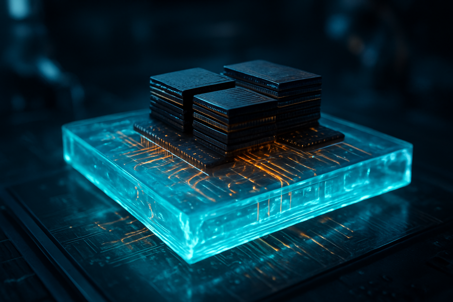
    The semiconductor industry has reached a historic inflection point as the world’s leading chipmakers—Intel, TSMC, and Samsung—officially move power routing to the "backside" of the silicon wafer. This architectural shift, known as Backside Power Delivery Network (BSPDN), represents the most significant change to transistor design in over a decade. By relocating the complex web of power-delivery wires from the top of the chip to the bottom, manufacturers are finally decoupling power from signal, effectively "flipping" the traditional chip architecture to unlock unprecedented levels of efficiency and performance.

    As of early 2026, this technology has transitioned from an experimental laboratory concept to the foundational engine of the AI revolution. With AI accelerators now pushing toward 1,000-watt power envelopes and consumer devices demanding more on-device intelligence than ever before, BSPDN has become the "lifeline" for the industry. Intel (NASDAQ: INTC) has taken an early lead with its PowerVia technology, while TSMC (NYSE: TSM) is preparing to counter with its more complex A16 process, setting the stage for a high-stakes battle over the future of high-performance computing.

    For the past fifty years, chips have been built like a house where the plumbing and the electrical wiring are all crammed into the ceiling, competing for space with the occupants. In traditional "front-side" power delivery, both signal-carrying wires and power-delivery wires are layered on top of the transistors. As transistors have shrunk to the 2nm and 1.6nm scales, this "spaghetti" of wiring has become a massive bottleneck, causing signal interference and significant voltage drops (IR drop) that waste energy and generate heat.

    Intel’s implementation, branded as PowerVia, solves this by using Nano-Through Silicon Vias (nTSVs) to route power directly from the back of the wafer to the transistors. This approach, debuted in the Intel 18A process, has already demonstrated a 30% reduction in voltage droop and a 15% improvement in performance-per-watt. By removing the power wires from the front side, Intel has also been able to pack transistors 30% more densely, as the signal wires no longer have to navigate around bulky power lines.

    TSMC’s approach, known as Super PowerRail (SPR), which is slated for mass production in the second half of 2026 on its A16 node, takes the concept even further. While Intel uses nTSVs to reach the transistor layer, TSMC’s SPR connects the power network directly to the source and drain of the transistors. This "direct-contact" method is significantly more difficult to manufacture but promises even better electrical characteristics, including an 8–10% speed gain at the same voltage and up to a 20% reduction in power consumption compared to its standard 2nm process.

    Initial reactions from the AI research community have been overwhelmingly positive. Experts at the 2026 International Solid-State Circuits Conference (ISSCC) noted that BSPDN effectively "resets the clock" on Moore’s Law. By thinning the silicon wafer to just a few micrometers to allow for backside routing, chipmakers have also inadvertently improved thermal management, as the heat-generating transistors are now physically closer to the cooling solutions on the back of the chip.

    The shift to backside power delivery is creating a new hierarchy among tech giants. NVIDIA (NASDAQ: NVDA), the undisputed leader in AI hardware, is reportedly the anchor customer for TSMC’s A16 process. While their current "Rubin" architecture pushed the limits of front-side delivery, the upcoming "Feynman" architecture is expected to leverage Super PowerRail to maintain its lead in AI training. The ability to deliver more power with less heat is critical for NVIDIA as it seeks to scale its Blackwell successors into massive, multi-die "superchips."

    Intel stands to benefit immensely from its first-mover advantage. By being the first to bring BSPDN to high-volume manufacturing with its 18A node, Intel has successfully attracted major foundry customers like Microsoft (NASDAQ: MSFT) and Amazon (NASDAQ: AMZN), both of which are designing custom AI silicon for their data centers. This "PowerVia-first" strategy has allowed Intel to position itself as a viable alternative to TSMC for the first time in years, potentially disrupting the existing foundry monopoly and shifting the balance of power in the semiconductor market.

    Apple (NASDAQ: AAPL) and AMD (NASDAQ: AMD) are also navigating this transition with high stakes. Apple is currently utilizing TSMC’s 2nm (N2) node for the iPhone 18 Pro, but reports suggest they are eyeing A16 for their 2027 "M5" and "A20" chips to support more advanced generative AI features on-device. Meanwhile, AMD is leveraging its chiplet expertise to integrate backside power into its "Instinct" MI400 series, aiming to close the performance gap with NVIDIA by utilizing the superior density and clock speeds offered by the new architecture.

    For startups and smaller AI labs, the arrival of BSPDN-enabled chips means more compute for every dollar spent on electricity. As power costs become the primary constraint for AI scaling, the 15-20% efficiency gains provided by backside power could be the difference between a viable business model and a failed venture. The competitive advantage will likely shift toward those who can most quickly adapt their software to take advantage of the higher clock speeds and increased core counts these new chips provide.

    Beyond the technical specifications, backside power delivery represents a fundamental shift in the broader AI landscape. We are moving away from an era where "more transistors" was the only metric that mattered, into an era of "system-level optimization." BSPDN is not just about making transistors smaller; it is about making the entire system—from the power supply to the cooling unit—more efficient. This mirrors previous milestones like the introduction of FinFET transistors or Extreme Ultraviolet (EUV) lithography, both of which were necessary to keep the industry moving forward when physical limits were reached.

    The environmental impact of this technology cannot be overstated. With data centers currently consuming an estimated 3-4% of global electricity—a figure projected to rise sharply due to AI demand—the efficiency gains from BSPDN are a critical component of the tech industry’s sustainability goals. A 20% reduction in power at the chip level translates to billions of kilowatt-hours saved across global AI clusters. However, this also raises concerns about "Jevons' Paradox," where increased efficiency leads to even greater demand, potentially offsetting the environmental benefits as companies simply build larger, more power-hungry models.

    There are also significant geopolitical implications. The race to master backside power delivery has become a centerpiece of national industrial policies. The U.S. government’s support for Intel’s 18A progress and the Taiwanese government’s backing of TSMC’s A16 development highlight how critical this technology is for national security and economic competitiveness. Being the first to achieve high yields on BSPDN nodes is now seen as a marker of a nation’s technological sovereignty in the age of artificial intelligence.

    Comparatively, the transition to backside power is being viewed as more disruptive than the move to 3D stacking (HBM). While HBM solved the "memory wall," BSPDN is solving the "power wall." Without it, the industry would have hit a hard ceiling where chips could no longer be cooled or powered effectively, regardless of how many transistors could be etched onto the silicon.

    Looking ahead, the next two years will see the integration of backside power delivery with other emerging technologies. The most anticipated development is the combination of BSPDN with Complementary Field-Effect Transistors (CFETs). By stacking n-type and p-type transistors on top of each other and powering them from the back, experts predict another 50% jump in density by 2028. This would allow for smartphone-sized devices with the processing power of today’s high-end workstations.

    In the near term, we can expect to see "backside signaling" experiments. Once the power is moved to the back, the front side of the chip is left entirely for signal routing. Researchers are already looking into moving some high-speed signal lines to the backside as well, which could further reduce latency and increase bandwidth for AI-to-AI communication. However, the primary challenge remains manufacturing yield. Thinning a wafer to the point where backside power is possible without destroying the delicate transistor structures is an incredibly precise process that will take years to perfect for mass production.

    Experts predict that by 2030, front-side power delivery will be viewed as an antique relic of the "early silicon age." The future of AI silicon lies in "true 3D" integration, where power, signal, and cooling are interleaved throughout the chip structure. As we move toward the 1nm and sub-1nm eras, the innovations pioneered by Intel and TSMC today will become the standard blueprint for every chip on the planet, enabling the next generation of autonomous systems, real-time translation, and personalized AI assistants.

    The shift to Backside Power Delivery marks the end of the "flat" era of semiconductor design. By moving the power grid to the back of the wafer, Intel and TSMC have broken through a physical barrier that threatened to stall the progress of artificial intelligence. The immediate results—higher clock speeds, better thermal management, and improved energy efficiency—are exactly what the industry needs to sustain the current pace of AI innovation.

    As we move through 2026, the key metrics to watch will be the production yields of Intel’s 18A and the first samples of TSMC’s A16. While Intel currently holds the "first-to-market" crown, the long-term winner will be the company that can manufacture these complex architectures at the highest volume with the fewest defects. This transition is not just a technical upgrade; it is a total reimagining of the silicon chip that will define the capabilities of AI for the next decade.

    In the coming weeks, keep an eye on the first independent benchmarks of Intel’s Panther Lake processors and any further announcements from NVIDIA regarding their Feynman architecture. The "Great Flip" has begun, and the world of computing will never look the same.


    This content is intended for informational purposes only and represents analysis of current AI developments.

    TokenRing AI delivers enterprise-grade solutions for multi-agent AI workflow orchestration, AI-powered development tools, and seamless remote collaboration platforms.
    For more information, visit https://www.tokenring.ai/.

  • The Silicon Rebellion: RISC-V Breaks the x86-ARM Duopoly to Power the AI Data Center

    The Silicon Rebellion: RISC-V Breaks the x86-ARM Duopoly to Power the AI Data Center

    The landscape of data center computing is undergoing its most significant architectural shift in decades. As of early 2026, the RISC-V open-source instruction set architecture (ISA) has officially graduated from its origins in embedded systems to become a formidable "third pillar" in the high-performance computing (HPC) and artificial intelligence markets. By providing a royalty-free, highly customizable alternative to the proprietary models of ARM and Intel (NASDAQ:INTC), RISC-V is enabling a new era of "silicon sovereignty" for hyperscalers and AI chip designers who are eager to bypass the restrictive licensing fees and "black box" designs of traditional vendors.

    The immediate significance of this development lies in the rapid maturation of server-grade RISC-V silicon. With the recent commercial availability of high-performance cores like Tenstorrent’s Ascalon and the strategic acquisition of Ventana Micro Systems by Qualcomm (NASDAQ:QCOM) in late 2025, the industry has signaled that RISC-V is no longer just a theoretical threat. It is now a primary contender for the massive AI inference and training workloads that define the modern data center, offering a level of architectural flexibility that neither x86 nor ARM can easily match in their current forms.

    Technical Breakthroughs: Vector Agnosticism and Chiplet Modularity

    The technical prowess of RISC-V in 2026 is anchored by the implementation of the RISC-V Vector (RVV) 1.0 extensions. Unlike the fixed-width SIMD (Single Instruction, Multiple Data) approaches found in Intel’s AVX-512 or ARM’s traditional NEON, RVV utilizes a vector-length agnostic (VLA) model. This allows software written for a 128-bit vector engine to run seamlessly on hardware with 512-bit or even 1024-bit vectors without the need for recompilation. For AI developers, this means a single software stack can scale across a diverse range of hardware, from edge devices to massive AI accelerators, significantly reducing the engineering overhead associated with hardware fragmentation.

    Leading the charge in raw performance is Tenstorrent’s Ascalon-X, an 8-wide decode, out-of-order superscalar core designed under the leadership of industry veteran Jim Keller. Benchmarks released in late 2025 show the Ascalon-X achieving approximately 22 SPECint2006/GHz, placing it in direct competition with the highest-tier cores from AMD (NASDAQ:AMD) and ARM. This performance is achieved through a modular chiplet architecture using the Universal Chiplet Interconnect Express (UCIe) standard, allowing designers to mix and match RISC-V cores with specialized AI accelerators and high-bandwidth memory (HBM) on a single package.

    Furthermore, the emergence of the RVA23 profile has standardized the features required for server-class operating systems, ensuring that Linux distributions and containerized workloads run with the same stability as they do on legacy architectures. Initial reactions from the AI research community have been overwhelmingly positive, particularly regarding the ability to add "custom instructions" to the ISA. This allows companies to bake proprietary AI mathematical kernels directly into the silicon, optimizing for specific Transformer-based models or emerging neural network architectures in ways that are physically impossible with the rigid instruction sets of x86 or ARM.

    Market Disruption: The End of the "ARM Tax"

    The expansion of RISC-V into the data center has sent shockwaves through the semiconductor industry, most notably affecting the strategic positioning of ARM. For years, hyperscalers like Amazon (NASDAQ:AMZN) and Alphabet (NASDAQ:GOOGL) have used ARM-based designs to reduce their reliance on Intel, but they remained tethered to ARM’s licensing fees and roadmap. The shift toward RISC-V represents a "declaration of independence" from these costs. Meta (NASDAQ:META) has already fully integrated RISC-V cores into its MTIA (Meta Training and Inference Accelerator) v3, using them for critical scalar and control tasks to optimize their massive social media recommendation engines.

    Qualcomm’s acquisition of Ventana Micro Systems in December 2025 is perhaps the clearest indicator of this market shift. By owning the high-performance RISC-V IP developed by Ventana, Qualcomm is positioning itself to offer cloud-scale server processors that are entirely free from ARM’s royalty structure. This move not only threatens ARM’s revenue streams but also forces a defensive consolidation among legacy players. In response, Intel and AMD formed a landmark "x86 Alliance" in late 2024 to standardize their own architectures, yet they struggle to match the rapid, community-driven innovation cycle that the open-source RISC-V ecosystem provides.

    Startups and regional players are also major beneficiaries. In China, Alibaba (NYSE:BABA) has utilized its T-Head semiconductor division to produce the XuanTie C930, a server-grade processor designed to circumvent Western export restrictions on high-end proprietary cores. By leveraging an open ISA, these companies can achieve "silicon sovereignty," ensuring that their national infrastructure is not dependent on the intellectual property of a single foreign corporation. This geopolitical advantage is driving a 60.9% compound annual growth rate (CAGR) for RISC-V in the data center, far outpacing the growth of its rivals.

    The Broader AI Landscape: A "Linux Moment" for Hardware

    The rise of RISC-V is often compared to the "Linux moment" for hardware. Just as open-source software democratized the server operating system market, RISC-V is democratizing the processor. This fits into the broader AI trend of moving away from general-purpose CPUs toward Domain-Specific Accelerators (DSAs). In an era where AI models are growing exponentially, the "one-size-fits-all" approach of x86 is becoming an energy-efficiency liability. RISC-V’s modularity allows for the creation of lean, highly specialized chips that do exactly what an AI workload requires and nothing more, leading to massive improvements in performance-per-watt.

    However, this shift is not without its concerns. The primary challenge remains software fragmentation. While the RISC-V Software Ecosystem (RISE) project—backed by Google, NVIDIA (NASDAQ:NVDA), and Samsung (KRX:005930)—has made enormous strides in porting compilers, libraries, and frameworks like PyTorch and TensorFlow, the "long tail" of enterprise legacy software still resides firmly on x86. Critics also point out that the open nature of the ISA could lead to a proliferation of incompatible "forks" if the community does not strictly adhere to the standards set by RISC-V International.

    Despite these hurdles, the comparison to previous milestones like the introduction of the first 64-bit processors is apt. RISC-V represents a fundamental change in how the industry thinks about compute. It is moving the value proposition away from the instruction set itself and toward the implementation and the surrounding ecosystem. This allows for a more competitive and innovative market where the best silicon design wins, rather than the one with the most entrenched licensing moat.

    Future Outlook: The Road to 2027 and Beyond

    Looking toward 2026 and 2027, the industry expects to see the first wave of "RISC-V native" supercomputers. These systems will likely utilize massive arrays of vector-optimized cores to handle the next generation of multimodal AI models. We are also on the verge of seeing RISC-V integrated into more complex "System-on-a-Chip" (SoC) designs for autonomous vehicles and robotics, where the same power-efficient AI inference capabilities used in the data center can be applied to real-time edge processing.

    The near-term challenges will focus on the maturation of the "northbound" software stack—ensuring that high-level orchestration tools like Kubernetes and virtualization layers work flawlessly with RISC-V’s unique vector extensions. Experts predict that by 2028, RISC-V will not just be a "companion" core in AI accelerators but will serve as the primary host CPU for a significant portion of new cloud deployments. The momentum is currently unstoppable, fueled by a global desire for open standards and the relentless demand for more efficient AI compute.

    Conclusion: A New Era of Open Compute

    The expansion of RISC-V into the data center marks a historic turning point in the evolution of artificial intelligence infrastructure. By breaking the x86-ARM duopoly, RISC-V has provided the industry with a path toward lower costs, greater customization, and true technological independence. The success of high-performance cores like the Ascalon-X and the strategic pivots by giants like Qualcomm and Meta demonstrate that the open-source hardware model is not only viable but essential for the future of hyperscale computing.

    In the coming weeks and months, industry watchers should keep a close eye on the first benchmarks of Qualcomm’s integrated Ventana designs and the progress of the RISE project’s software optimization efforts. As more enterprises begin to pilot RISC-V based instances in the cloud, the "third pillar" will continue to solidify its position. The long-term impact will be a more diverse, competitive, and innovative semiconductor landscape, ensuring that the hardware of tomorrow is as open and adaptable as the AI software it powers.


    This content is intended for informational purposes only and represents analysis of current AI developments.

    TokenRing AI delivers enterprise-grade solutions for multi-agent AI workflow orchestration, AI-powered development tools, and seamless remote collaboration platforms.
    For more information, visit https://www.tokenring.ai/.

  • The Era of Light: Photonic Interconnects Shatter the ‘Copper Wall’ in AI Scaling

    The Era of Light: Photonic Interconnects Shatter the ‘Copper Wall’ in AI Scaling

    As of January 9, 2026, the artificial intelligence industry has officially reached a historic architectural milestone: the transition from electricity to light as the primary medium for data movement. For decades, copper wiring has been the backbone of computing, but the relentless demands of trillion-parameter AI models have finally pushed electrical signaling to its physical breaking point. This phenomenon, known as the "Copper Wall," threatened to stall the growth of AI clusters just as the world moved toward the million-GPU era.

    The solution, now being deployed in high-volume production across the globe, is Photonic Interconnects. By integrating Optical I/O (Input/Output) directly into the silicon package, companies are replacing traditional electrical pins with microscopic lasers and light-modulating chiplets. This shift is not merely an incremental upgrade; it represents a fundamental decoupling of compute performance from the energy and distance constraints of electricity, enabling a 70% reduction in interconnect power and a 10x increase in bandwidth density.

    Breaking the I/O Tax: The Technical Leap to 5 pJ/bit

    The technical crisis that precipitated this revolution was the "I/O Tax"—the massive amount of energy required simply to move data between GPUs. In legacy 2024-era clusters, moving data across a rack could consume up to 30% of a system's total power budget. At the new 224 Gbps and 448 Gbps per-lane data rates required for 2026 workloads, copper signals degrade after traveling just a few inches. Optical I/O solves this by converting electrons to photons at the "shoreline" of the chip. This allows data to travel hundreds of meters with virtually no signal loss and minimal heat generation.

    Leading the charge in technical specifications is Lightmatter, whose Passage M1000 platform has become a cornerstone of the 2026 AI data center. Unlike previous Co-Packaged Optics (CPO) that placed optical engines at the edge of a chip, Lightmatter’s 3D photonic interposer allows GPUs to sit directly on top of a photonic layer. This enables a record-breaking 114 Tbps of aggregate bandwidth and a bandwidth density of 1.4 Tbps/mm². Meanwhile, Ayar Labs has moved into high-volume production of its TeraPHY Gen 3 chiplets, which are the first to carry Universal Chiplet Interconnect Express (UCIe) traffic optically, achieving power efficiencies as low as 5 picojoules per bit (pJ/bit).

    This new approach differs fundamentally from the "pluggable" transceivers of the past. In previous generations, optical modules were bulky components plugged into the front of a switch. In the 2026 paradigm, the laser source is often external for serviceability (standardized as ELSFP), but the modulation and detection happen inside the GPU or Switch package itself. This "Direct Drive" architecture eliminates the need for power-hungry Digital Signal Processors (DSPs), which were a primary source of latency and heat in earlier optical attempts.

    The New Power Players: NVIDIA, Broadcom, and the Marvell-Celestial Merger

    The shift to photonics has redrawn the competitive map of the semiconductor industry. NVIDIA (NASDAQ: NVDA) signaled its dominance in this new era at CES 2026 with the official launch of the Rubin platform. Rubin makes optical I/O a core requirement, utilizing Spectrum-X Ethernet Photonics and Quantum-X800 InfiniBand switches. By integrating silicon photonic engines developed with TSMC (NYSE: TSM) directly into the switch ASIC, NVIDIA has achieved a 5x power reduction per 1.6 Tb/s port, ensuring their "single-brain" cluster architecture can scale to millions of interconnected nodes.

    Broadcom (NASDAQ: AVGO) has also secured a massive lead with its Tomahawk 6 (Davisson) switch, which began volume shipping in late 2025. The TH6-Davisson is a behemoth, boasting 102.4 Tbps of total switching capacity. By utilizing integrated 6.4 Tbps optical engines, Broadcom has effectively cornered the market for hyperscale Ethernet backbones. Not to be outdone, Marvell (NASDAQ: MRVL) made a seismic move in early January 2026 by announcing the $3.25 billion acquisition of Celestial AI. This merger combines Marvell’s robust CXL and PCIe switching portfolio with Celestial’s "Photonic Fabric," a technology specifically designed for optical memory pooling, allowing GPUs to share HBM4 memory across a rack at light speed.

    For startups and smaller AI labs, this development is a double-edged sword. While photonic interconnects lower the long-term operational costs of AI clusters by slashing energy bills, the capital expenditure required to build light-based infrastructure is significantly higher. This reinforces the strategic advantage of "Big Tech" hyperscalers like Amazon (NASDAQ: AMZN) and Google (NASDAQ: GOOGL), who have the capital to transition their entire fleets to photonic-ready architectures.

    A Paradigm Shift: From Moore’s Law to the Million-GPU Cluster

    The wider significance of photonic interconnects cannot be overstated. For years, industry observers feared that Moore’s Law was reaching a hard limit—not because we couldn't make smaller transistors, but because we couldn't get data to those transistors fast enough without melting the chip. The "interconnect bottleneck" was the single greatest threat to the continued scaling of Large Language Models (LLMs) and World Models. By moving to light, the industry has bypassed this physical wall, effectively extending the roadmap for AI scaling for another decade.

    This transition also addresses the growing global concern over the energy consumption of AI data centers. By reducing the power required for data movement by 70%, photonics provides a much-needed "green" dividend. However, this breakthrough also brings new concerns, particularly regarding the complexity of the supply chain. The manufacturing of silicon photonics requires specialized cleanrooms and high-precision packaging techniques that are currently concentrated in a few locations, such as TSMC’s advanced packaging facilities in Taiwan.

    Comparatively, the move to Optical I/O is being viewed as a milestone on par with the introduction of the GPU itself. If the GPU gave AI its "brain," photonic interconnects are giving it a "nervous system" capable of near-instantaneous communication across vast distances. This enables the transition from isolated servers to "warehouse-scale computers," where the entire data center functions as a single, coherent processing unit.

    The Road to 2027: All-Optical Computing and Beyond

    Looking ahead, the near-term focus will be on the refinement of Co-Packaged Optics and the stabilization of external laser sources. Experts predict that by 2027, we will see the first "all-optical" switch fabrics where data is never converted back into electrons between the source and the destination. This would further reduce latency to the absolute limits of the speed of light, enabling real-time training of models that are orders of magnitude larger than GPT-5.

    Potential applications on the horizon include "Disaggregated Memory," where banks of high-speed memory can be located in a separate part of the data center from the processors, connected via optical fabric. This would allow for much more flexible and efficient use of expensive hardware resources. Challenges remain, particularly in the yield rates of integrated photonic chiplets and the long-term reliability of microscopic lasers, but the industry's massive R&D investment suggests these are hurdles, not roadblocks.

    Summary: A New Foundation for Intelligence

    The revolution in photonic interconnects marks the end of the "Copper Age" of high-performance computing. Key takeaways from this transition include the massive 70% reduction in I/O power, the rise of 100+ Tbps switching capacities, and the dominance of integrated silicon photonics in the roadmaps of industry leaders like NVIDIA, Broadcom, and Intel (NASDAQ: INTC).

    This development will likely be remembered as the moment when AI scaling became decoupled from the physical constraints of electricity. In the coming months, watch for the first performance benchmarks from NVIDIA’s Rubin clusters and the finalized integration of Celestial AI’s fabric into Marvell’s silicon. The "Era of Light" is no longer a futuristic concept; it is the current reality of the global AI infrastructure.


    This content is intended for informational purposes only and represents analysis of current AI developments.

    TokenRing AI delivers enterprise-grade solutions for multi-agent AI workflow orchestration, AI-powered development tools, and seamless remote collaboration platforms.
    For more information, visit https://www.tokenring.ai/.