In a landmark keynote at the 2026 Consumer Electronics Show (CES) in Las Vegas, NVIDIA (NASDAQ: NVDA) CEO Jensen Huang officially introduced the "Vera Rubin" architecture, a comprehensive platform redesign that signals the most aggressive expansion of AI compute power in the company’s history. Named after the pioneering astronomer who confirmed the existence of dark matter, the Rubin platform is not merely a component upgrade but a full-stack architectural overhaul designed to power the next generation of "agentic AI" and trillion-parameter models.
The announcement marks a historic shift for the semiconductor industry as NVIDIA formalizes its transition to a yearly release cadence. By moving from a multi-year cycle to an annual "Blackwell-to-Rubin" pace, NVIDIA is effectively challenging the rest of the industry to match its blistering speed of innovation. With the Vera Rubin platform slated for full production in the second half of 2026, the tech giant is positioning itself to remain the indispensable backbone of the global AI economy.
Breaking the Memory Wall: Technical Specifications of the Rubin Platform
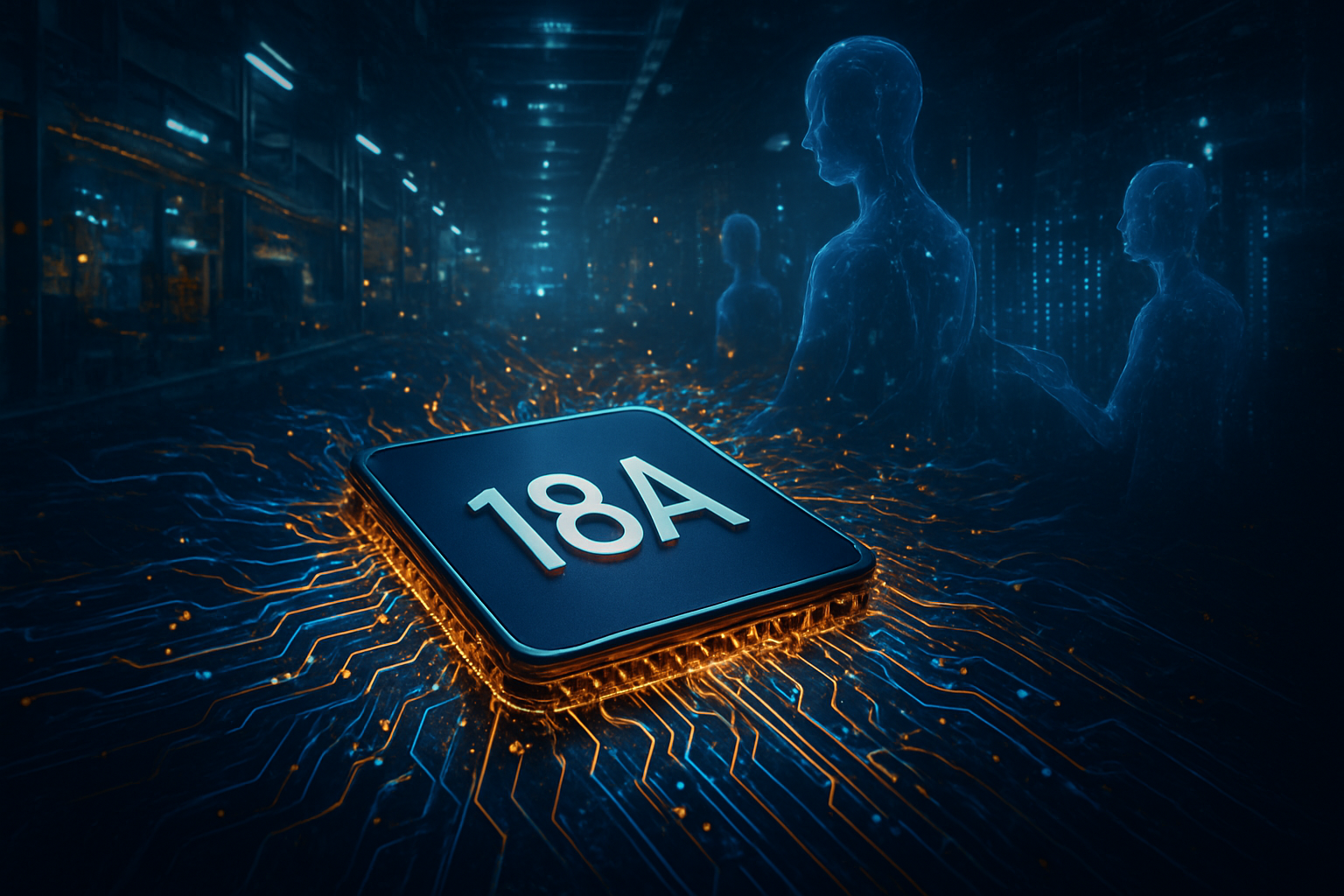
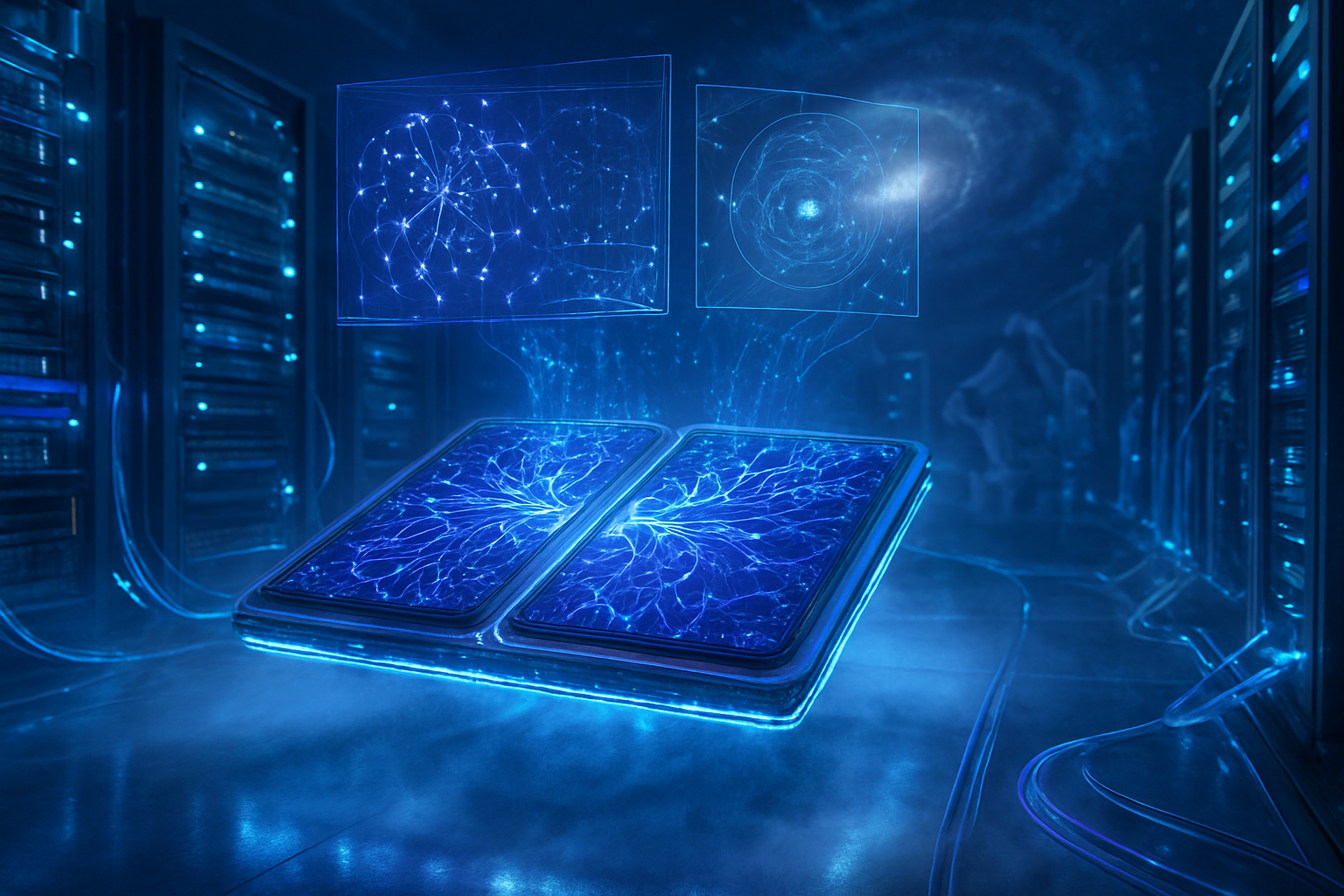
The heart of the new architecture lies in the Rubin GPU, a massive 336-billion transistor processor built on a cutting-edge 3nm process from TSMC (NYSE: TSM). For the first time, NVIDIA is utilizing a dual-die "reticle-sized" package that functions as a single unified accelerator, delivering an astonishing 50 PFLOPS of inference performance at NVFP4 precision. This represents a five-fold increase over the Blackwell architecture released just two years prior. Central to this leap is the transition to HBM4 memory, with each Rubin GPU sporting up to 288GB of high-bandwidth memory. By utilizing a 2048-bit interface, Rubin achieves an aggregate bandwidth of 22 TB/s per GPU, a crucial advancement for overcoming the "memory wall" that has previously bottlenecked large-scale Mixture-of-Experts (MoE) models.
Complementing the GPU is the newly unveiled Vera CPU, which replaces the previous Grace architecture with custom-designed "Olympus" Arm (NASDAQ: ARM) cores. The Vera CPU features 88 high-performance cores with Spatial Multi-Threading (SMT) support, doubling the L2 cache per core compared to its predecessor. This custom silicon is specifically optimized for data orchestration and managing the complex workflows required by autonomous AI agents. The connection between the Vera CPU and Rubin GPU is facilitated by the second-generation NVLink-C2C, providing a 1.8 TB/s coherent memory space that allows the two chips to function as a singular, highly efficient super-processor.
The technical community has responded with a mixture of awe and strategic concern. Industry experts at the show highlighted the "token-to-power" efficiency of the Rubin platform, noting that the third-generation Transformer Engine's hardware-accelerated adaptive compression will be vital for making 100-trillion-parameter models economically viable. However, researchers also point out that the sheer density of the Rubin architecture necessitates a total move toward liquid-cooled data centers, as the power requirements per rack continue to climb into the hundreds of kilowatts.
Strategic Disruption and the Annual Release Paradigm
NVIDIA’s shift to a yearly release cadence—moving from Hopper (2022) to Blackwell (2024), Blackwell Ultra (2025), and now Rubin (2026)—is a strategic masterstroke that places immense pressure on competitors like AMD (NASDAQ: AMD) and Intel (NASDAQ: INTC). By shortening the lifecycle of its flagship products, NVIDIA is forcing cloud service providers (CSPs) and enterprise customers into a continuous upgrade cycle. This "perpetual innovation" strategy ensures that the latest frontier models are always developed on NVIDIA hardware, making it increasingly difficult for startups or rival labs to gain a foothold with alternative silicon.
Major infrastructure partners, including Dell Technologies (NYSE: DELL) and Super Micro Computer (NASDAQ: SMCI), are already pivoting to support the Rubin NVL72 rack-scale systems. These 100% liquid-cooled racks are designed to be "cableless" and modular, with NVIDIA claiming that deployment times for a full cluster have dropped from several hours to just five minutes. This focus on "the rack as the unit of compute" allows NVIDIA to capture a larger share of the data center value chain, effectively selling entire supercomputers rather than just individual chips.
The move also creates a supply chain "arms race." Memory giants such as SK Hynix (KRX: 000660) and Micron (NASDAQ: MU) are now operating on accelerated R&D schedules to meet NVIDIA’s annual demands for HBM4. While this benefits the semiconductor ecosystem's revenue, it raises concerns about "buyer's remorse" for enterprises that invested heavily in Blackwell systems only to see them surpassed within 12 months. Nevertheless, for major AI labs like OpenAI and Anthropic, the Rubin platform's ability to handle the next generation of reasoning-heavy AI agents is a competitive necessity that outweighs the rapid depreciation of older hardware.
The Broader AI Landscape: From Chatbots to Autonomous Agents
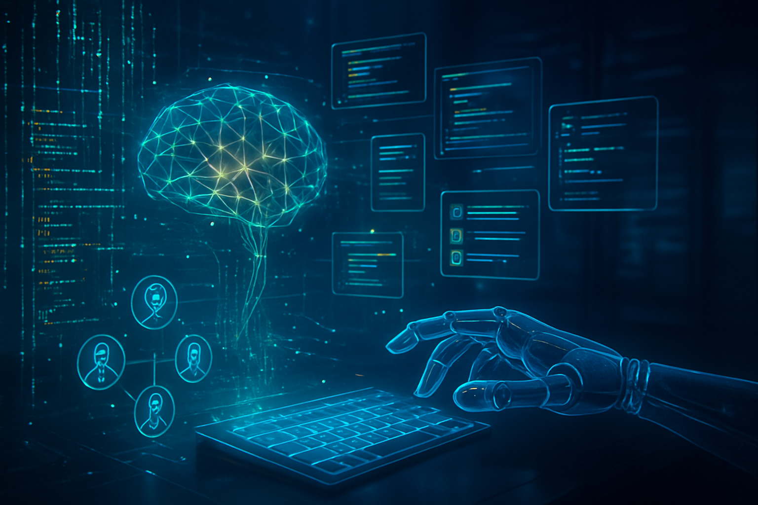
The Vera Rubin architecture arrives at a pivotal moment in the AI trajectory, as the industry moves away from simple generative chatbots toward "Agentic AI"—systems capable of multi-step reasoning, tool use, and autonomous problem-solving. These agents require massive amounts of "Inference Context Memory," a challenge NVIDIA is addressing with the BlueField-4 DPU. By offloading KV cache data and managing infrastructure tasks at the chip level, the Rubin platform enables agents to maintain much larger context windows, allowing them to remember and process complex project histories without a performance penalty.
This development mirrors previous industry milestones, such as the introduction of the CUDA platform or the launch of the H100, but at a significantly larger scale. The Rubin platform is essentially the hardware manifestation of the "Scaling Laws," proving that NVIDIA believes more compute and more bandwidth remain the primary paths to Artificial General Intelligence (AGI). By integrating ConnectX-9 SuperNICs and Spectrum-6 Ethernet Switches into the platform, NVIDIA is also solving the "scale-out" problem, allowing thousands of Rubin GPUs to communicate with the low latency required for real-time collaborative AI.
However, the wider significance of the Rubin launch also brings environmental and accessibility concerns to the forefront. The power density of the NVL72 racks means that only the most modern, liquid-cooled data centers can house these systems, potentially widening the gap between "compute-rich" tech giants and "compute-poor" academic institutions or smaller nations. As NVIDIA cements its role as the gatekeeper of high-end AI compute, the debate over the centralization of AI power is expected to intensify throughout 2026.
Future Horizons: The Path Beyond Rubin
Looking ahead, NVIDIA’s roadmap suggests that the Rubin architecture is just the beginning of a new era of "Physical AI." During the CES keynote, Huang teased future iterations, likely to be dubbed "Rubin Ultra," which will further refine the 3nm process and explore even more advanced packaging techniques. The long-term goal appears to be the creation of a "World Engine"—a computing platform capable of simulating the physical world in real-time to train autonomous robots and self-driving vehicles in high-fidelity digital twins.
The challenges remaining are primarily physical and economic. As chips approach the limits of Moore’s Law, NVIDIA is increasingly relying on "system-level" scaling. This means the future of AI will depend as much on innovations in liquid cooling and power delivery as it does on transistor density. Experts predict that the next two years will see a massive surge in the construction of specialized "AI factories"—data centers built from the ground up specifically to house Rubin-class hardware—as enterprises move from experimental AI to full-scale autonomous operations.
Conclusion: A New Standard for the AI Era
The launch of the Vera Rubin architecture at CES 2026 represents a definitive moment in the history of computing. By delivering a 5x leap in inference performance and introducing the first true HBM4-powered platform, NVIDIA has not only raised the bar for technical excellence but has also redefined the speed at which the industry must operate. The transition to an annual release cadence ensures that NVIDIA remains at the center of the AI universe, providing the essential infrastructure for the transition from generative models to autonomous agents.
Key takeaways from the announcement include the critical role of the Vera CPU in managing agentic workflows, the staggering 22 TB/s memory bandwidth of the Rubin GPU, and the shift toward liquid-cooled, rack-scale units as the standard for enterprise AI. As the first Rubin systems begin shipping later this year, the tech world will be watching closely to see how these advancements translate into real-world breakthroughs in scientific research, autonomous systems, and the quest for AGI. For now, one thing is clear: the Rubin era has arrived, and the pace of AI development is only getting faster.
This content is intended for informational purposes only and represents analysis of current AI developments.
TokenRing AI delivers enterprise-grade solutions for multi-agent AI workflow orchestration, AI-powered development tools, and seamless remote collaboration platforms.
For more information, visit https://www.tokenring.ai/.