Category: Uncategorized

  • The Age of the Agent: OpenAI’s GPT-5.2 Shatters Benchmarks and Redefines Professional Productivity

    The Age of the Agent: OpenAI’s GPT-5.2 Shatters Benchmarks and Redefines Professional Productivity

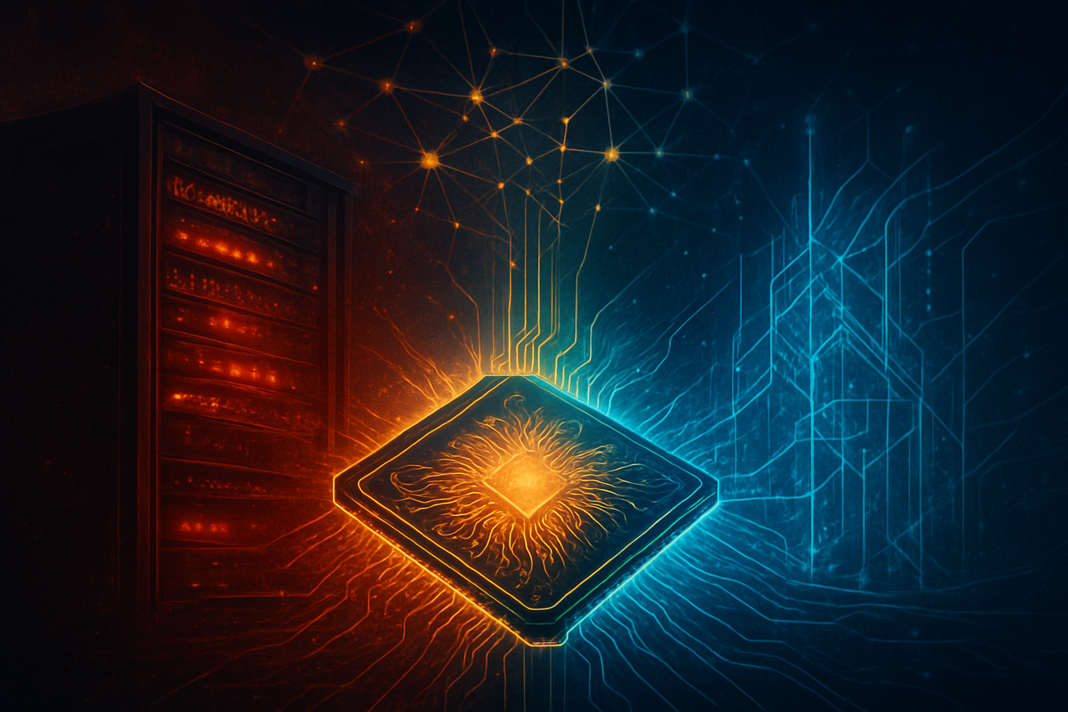
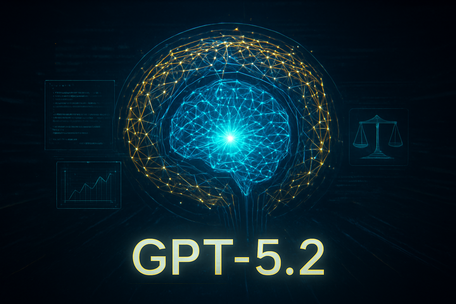
    The artificial intelligence landscape underwent a seismic shift on December 11, 2025, with the release of OpenAI’s GPT-5.2. Positioned as a "professional agentic" tool rather than a mere conversationalist, GPT-5.2 represents the most significant leap in machine reasoning since the original debut of GPT-4. This latest iteration is designed to move beyond simple text generation, functioning instead as a high-fidelity reasoning engine capable of managing complex, multi-step workflows with a level of autonomy that was previously the stuff of science fiction.

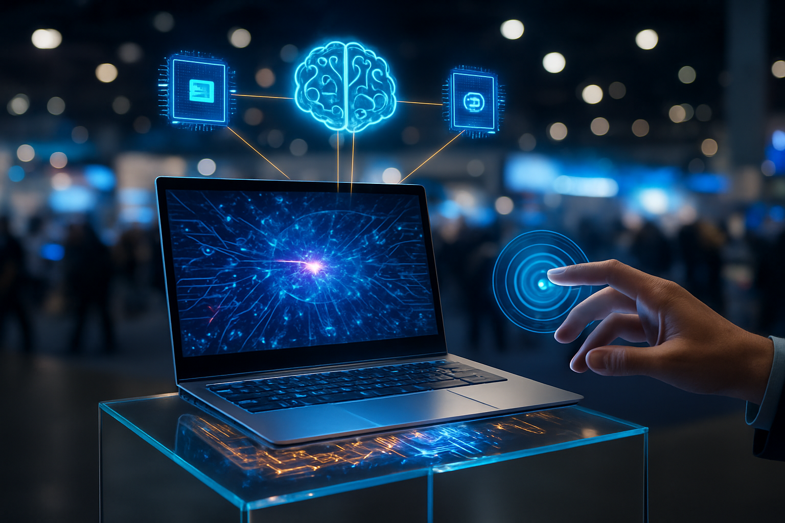
    The immediate significance of this release cannot be overstated. By introducing a tiered architecture—Instant, Thinking, and Pro—OpenAI has effectively created a "gearbox" for intelligence, allowing users to modulate the model's cognitive load based on the task at hand. Early industry feedback suggests that GPT-5.2 is not just an incremental update; it is a foundational change in how businesses approach cognitive labor. With a 30% reduction in factual errors and a performance profile that frequently matches or exceeds human professionals, the model has set a new standard for reliability and expert-level output in the enterprise sector.

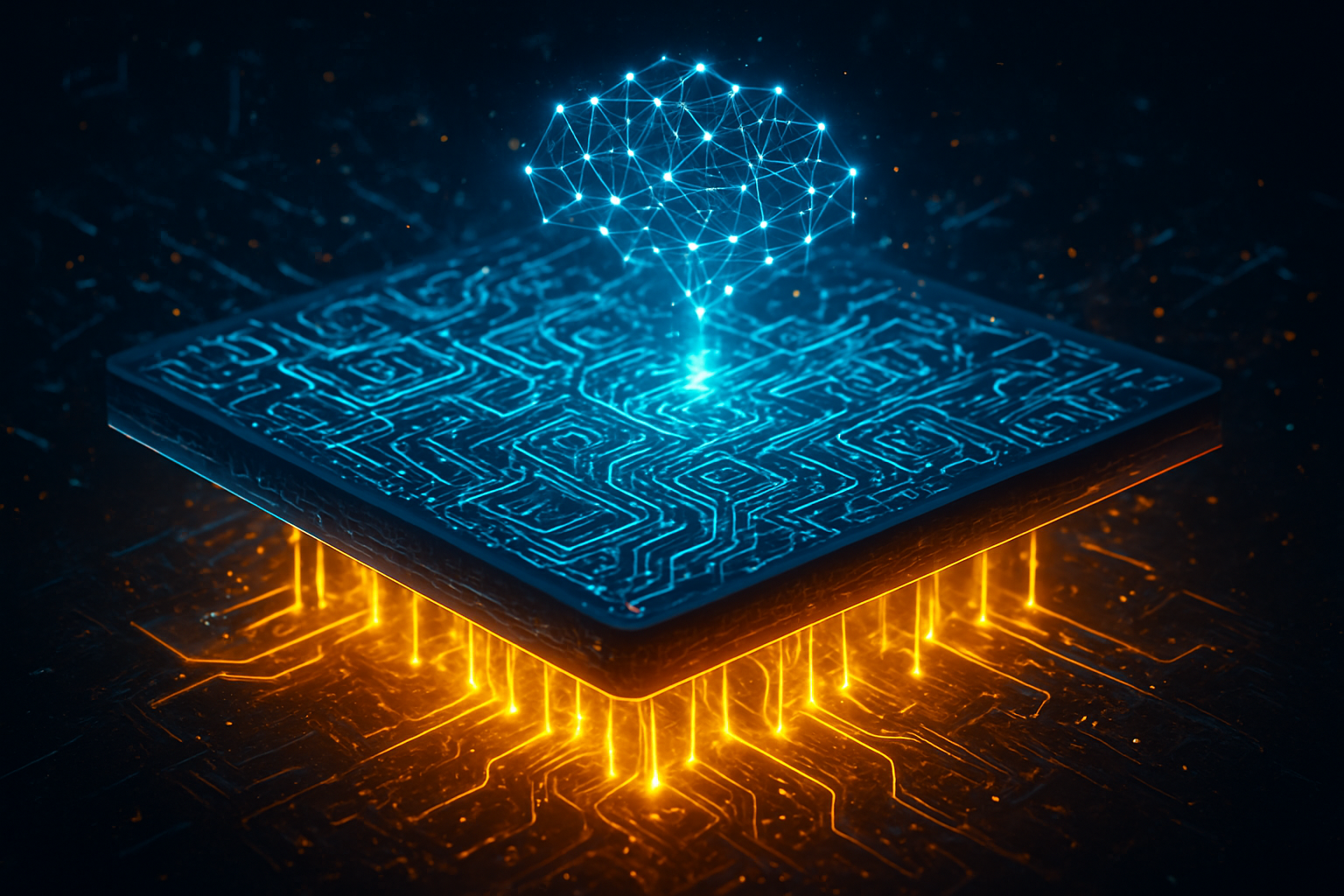
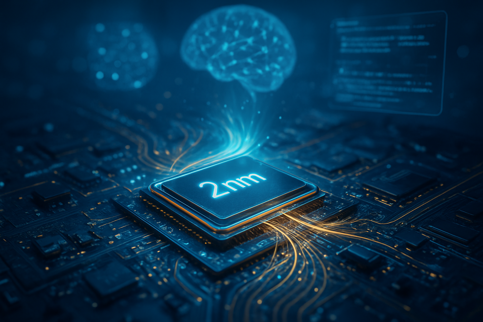
    Technically, GPT-5.2 is a marvel of efficiency and depth. At the heart of the release is the Thinking version, which utilizes a dynamic "Reasoning Effort" parameter. This allows the model to "deliberate" internally before providing an answer, providing a transparent summary of its internal logic via a Chain of Thought output. In the realm of software engineering, GPT-5.2 Thinking achieved a record-breaking score of 55.6% on the SWE-Bench Pro benchmark—a rigorous, multi-language evaluation designed to resist data contamination. A specialized variant, GPT-5.2-Codex, pushed this even further to 56.4%, demonstrating an uncanny ability to resolve complex GitHub issues and system-level bugs that previously required senior-level human intervention.

    Perhaps more vital for enterprise adoption is the dramatic 30% reduction in factual errors compared to its predecessor, GPT-5.1. This was achieved through a combination of enhanced retrieval-augmented generation (RAG) and a new "verification layer" that cross-references internal outputs against high-authority knowledge bases in real-time. The flagship Pro version takes this a step further, offering a massive 400,000-token context window and an exclusive "xhigh" reasoning level. This mode allows the model to spend several minutes on a single prompt, effectively "thinking through" high-stakes problems in fields like legal discovery, medical diagnostics, and system architecture.

    The Instant version rounds out the family, optimized for ultra-low latency. While it lacks the deep reasoning of its siblings, it boasts a 40% reduction in hallucinations for routine tasks, making it the ideal "reflexive" brain for real-time applications like live translation and scheduling. Initial reactions from the AI research community have been overwhelmingly positive, with many experts noting that the "Thinking" model's ability to show its work provides a much-needed layer of interpretability that has been missing from previous frontier models.

    The market implications of GPT-5.2 were felt immediately across the tech sector. Microsoft (NASDAQ: MSFT), OpenAI’s primary partner, integrated the model into its Microsoft 365 Copilot suite within hours of the announcement. By late December, Microsoft began rebranding Windows 11 as an "agentic OS," leveraging GPT-5.2 to allow users to control system settings and execute complex file management tasks via natural language. This move has placed immense pressure on Alphabet Inc. (NASDAQ: GOOGL), which responded by accelerating the rollout of Gemini 3’s "Deep Think Mode" across 800 million Samsung (KRX: 005930) Galaxy devices.

    The competitive landscape is also forcing defensive maneuvers from other tech giants. Meta Platforms, Inc. (NASDAQ: META), seeking to bridge the gap in autonomous agent capabilities, reportedly acquired the Singapore-based agentic startup Manus AI for $2 billion following the GPT-5.2 release. Meanwhile, Anthropic remains a fierce competitor; its Claude 4.5 model continues to hold a slight edge in certain coding leaderboards, maintaining its position as the preferred choice for safety-conscious enterprises. However, the sheer breadth of OpenAI’s "gearbox" approach—offering high-speed, high-reasoning, and deep-work tiers—gives them a strategic advantage in capturing diverse market segments from developers to C-suite executives.

    Beyond the technical and corporate rivalry, the wider significance of GPT-5.2 lies in its economic potential, as highlighted by the new GDPval benchmark. Designed by OpenAI to measure performance on economically valuable tasks, GPT-5.2 Thinking outperformed industry professionals in 70.9% of comparisons across 44 occupations, including accounting, law, and manufacturing. The model completed these tasks roughly 11 times faster than human experts at less than 1% of the cost. This represents a pivotal moment in the "AI for work" trend, suggesting that AI is no longer just assisting professionals but is now capable of performing core professional duties at an expert level.

    This breakthrough does not come without concerns. The ability of GPT-5.2 to outperform professionals across nearly four dozen occupations has reignited debates over labor displacement and the necessity of universal basic income (UBI) frameworks. On abstract reasoning tests like ARC-AGI-2, the model scored 54.2%, nearly triple the performance of previous generations, signaling that AI is rapidly closing the gap on general intelligence. This milestone compares to the historical significance of Deep Blue defeating Garry Kasparov, but with the added complexity that this "intelligence" is now being deployed across every sector of the global economy simultaneously.

    Looking ahead, the near-term focus will be on the "agentic" deployment of these models. Experts predict that the next 12 months will see a proliferation of autonomous AI workers capable of managing entire departments, from customer support to software QA, with minimal human oversight. The challenge for 2026 will be addressing the "alignment gap"—ensuring that as these models spend more time "thinking" and acting independently, they remain strictly within the bounds of human intent and safety protocols.

    We also expect to see a shift in hardware requirements. As GPT-5.2 Pro utilizes minutes of compute for a single query, the demand for specialized AI inference chips will likely skyrocket, further benefiting companies like NVIDIA (NASDAQ: NVDA). In the long term, the success of GPT-5.2 serves as a precursor to GPT-6, which is rumored to incorporate even more advanced "world models" that allow the AI to simulate outcomes in physical environments, potentially revolutionizing robotics and automated manufacturing.

    OpenAI’s GPT-5.2 release marks the definitive end of the "chatbot era" and the beginning of the "agentic era." By delivering a model that can think, reason, and act with professional-grade precision, OpenAI has fundamentally altered the trajectory of human-computer interaction. The key takeaways are clear: the reduction in factual errors and the massive jump in coding and reasoning benchmarks make AI a reliable partner for high-stakes professional work.

    As we move deeper into 2026, the industry will be watching how competitors like Google and Anthropic respond to this "gearbox" approach to intelligence. The significance of GPT-5.2 in AI history will likely be measured by how quickly society can adapt to its presence. For now, one thing is certain: the bar for what constitutes "artificial intelligence" has once again been raised, and the world is only beginning to understand the implications.


    This content is intended for informational purposes only and represents analysis of current AI developments.

    TokenRing AI delivers enterprise-grade solutions for multi-agent AI workflow orchestration, AI-powered development tools, and seamless remote collaboration platforms.
    For more information, visit https://www.tokenring.ai/.

  • Texas Bolsters Semiconductor Sovereignty with $15.2 Million Grant for Tekscend Photomask Expansion

    Texas Bolsters Semiconductor Sovereignty with $15.2 Million Grant for Tekscend Photomask Expansion

    In a decisive move to fortify the domestic semiconductor supply chain, Texas Governor Greg Abbott announced today, January 14, 2026, a $15.2 million grant from the Texas Semiconductor Innovation Fund (TSIF) to Tekscend Photomask Round Rock Inc. The investment serves as the cornerstone for a massive $223 million expansion of the company’s manufacturing facility in Round Rock, Texas. This expansion is designed to secure the production of critical photomasks—the ultra-precise stencils used to etch circuit patterns onto silicon—ensuring that the "Silicon Hills" of Central Texas remain at the forefront of global chip production.

    The announcement marks a pivotal moment in the ongoing global re-shoring effort, as the United States seeks to reduce its reliance on East Asian manufacturing for foundational hardware components. By boosting the capacity of the Round Rock site by over 40%, the project addresses a significant bottleneck in the semiconductor lifecycle. As industry leaders often remark, "No masks, no chips," and this investment ensures that the essential first step of chip fabrication stays firmly on American soil.

    Technical Milestones: From 12nm Nodes to High-NA EUV

    The technical heart of the $223 million expansion lies in its focus on the 12nm technology node and beyond. Photomasks are master templates used in the lithography process; they contain the microscopic circuit designs that are projected onto wafers. As chip geometries shrink, the requirements for mask precision become exponentially more demanding. The Tekscend expansion will modernize existing infrastructure to handle the complexities of 12nm production, which is a critical sweet spot for chips powering automotive systems, industrial automation, and the burgeoning Internet of Things (IoT) landscape.

    Beyond the 12nm commercial threshold, Tekscend—the global entity Tekscend Photomask Corp. (TSE: 429A)—is pushing the boundaries of physics. While the Round Rock facility stabilizes the mid-range supply, the company’s recent joint development agreement with IBM (NYSE: IBM) has already begun paving the way for 2nm logic nodes and High-Numerical Aperture (High-NA) Extreme Ultraviolet (EUV) lithography. This dual-track strategy ensures that while the U.S. secures its current industrial needs, the foundational research for the next generation of sub-5nm chips is deeply integrated into the domestic ecosystem.

    Industry experts note that this development differs from previous expansion efforts due to its focus on "advanced-mature" nodes. While much of the federal CHIPS Act funding has targeted leading-edge 2nm and 3nm fabs, the TSIF grant recognizes that 12nm production is vital for national security and economic stability. By modernizing equipment and increasing throughput, Tekscend is bridging the gap between legacy manufacturing and the ultra-advanced future of AI hardware.

    Strategic Advantage and the "Silicon Hills" Ecosystem

    The re-shoring of photomask production provides an immense strategic advantage to neighboring semiconductor giants. Major players such as Samsung Electronics (KRX: 005930), which is currently expanding its presence in Taylor and Austin, and Texas Instruments (NASDAQ: TXN), with its extensive operations in North and Central Texas, stand to benefit from a localized, high-capacity mask supplier. Reducing the transit time and geopolitical risk associated with importing masks from overseas allows these companies to accelerate their prototyping and production cycles significantly.

    For the broader tech market, this development signals a cooling of the "supply chain anxiety" that has gripped the industry since 2020. By localizing the production of 12nm masks, Tekscend mitigates the risk of sudden disruptions in the Asia-Pacific region. This move also creates a competitive moat for U.S.-based fabless designers who can now rely on a domestic partner for the most sensitive part of their intellectual property—the physical layout of their chips.

    Market analysts suggest that Tekscend’s recent IPO on the Tokyo Stock Exchange and its rebranding from Toppan Photomasks have positioned it as an agile, independent power in the lithography space. With a current valuation of approximately $2 billion, the company is leveraging regional incentives like the TSIF to outmaneuver competitors who remain tethered to centralized, offshore manufacturing hubs.

    The Global Significance of Semiconductor Re-shoring

    This grant is one of the first major disbursements from the Texas Semiconductor Innovation Fund, a multi-billion dollar initiative designed to complement the federal U.S. CHIPS & Science Act. It highlights a growing trend where state governments are taking a proactive role in geopolitical industrial policy. The shift toward a "continental supply chain" is no longer just a theoretical goal; it is a funded reality that seeks to counteract China’s massive investments in its own domestic semiconductor infrastructure.

    The broader significance lies in the concept of "sovereign silicon." As AI continues to integrate into every facet of modern life—from defense systems to healthcare diagnostics—the ability to produce the hardware required for AI without foreign interference is a matter of national importance. The Tekscend expansion serves as a proof-of-concept for how specialized components of the supply chain, often overlooked in favor of high-profile fab announcements, are being systematically brought back to the U.S.

    However, the transition is not without challenges. The expansion requires at least 50 new high-skilled roles in an already tight labor market. The success of this initiative will depend largely on the ability of the Texas educational system to produce the specialized engineers and technicians required to operate the sophisticated lithography equipment being installed in Round Rock.

    Future Outlook and the Road to 2030

    Looking ahead, the Round Rock facility is expected to be fully operational with its expanded capacity by late 2027. In the near term, we can expect a surge in local production for automotive and AI-edge chips. In the long term, the partnership between Tekscend and IBM suggests that the technology perfected in these labs today will eventually find its way into the high-volume manufacturing lines of the 2030s.

    Predicting the next steps, experts anticipate further TSIF grants targeting other "bottleneck" sectors of the supply chain, such as advanced packaging and specialty chemicals. The goal is to create a closed-loop ecosystem in Texas where a chip can be designed, masked, fabricated, and packaged within a 100-mile radius. This level of vertical integration would make the Central Texas region the most resilient semiconductor hub in the world.

    Conclusion: A Milestone for Domestic Innovation

    The $15.2 million grant to Tekscend Photomask is more than just a financial boost for a local business; it is a vital brick in the wall of American technological independence. By securing the production of 12nm photomasks, Texas is ensuring that the state remains the "brain" of the global semiconductor industry. The project's $223 million total investment reflects a long-term commitment to the infrastructure that makes modern computing possible.

    As we move through 2026, the industry will be watching the progress of the Round Rock facility closely. The success of this expansion will serve as a bellwether for the efficacy of state-led industrial funds and the feasibility of large-scale re-shoring. For now, the message from the "Silicon Hills" is clear: the United States is reclaiming the tools of its own innovation, one mask at a time.


    This content is intended for informational purposes only and represents analysis of current AI and semiconductor developments.

    TokenRing AI delivers enterprise-grade solutions for multi-agent AI workflow orchestration, AI-powered development tools, and seamless remote collaboration platforms.
    For more information, visit https://www.tokenring.ai/.

  • The DeepSeek Effect: How Ultra-Efficient Models Cracked the Code of Semiconductor “Brute Force”

    The DeepSeek Effect: How Ultra-Efficient Models Cracked the Code of Semiconductor “Brute Force”

    The artificial intelligence industry is currently undergoing its most significant structural shift since the "Attention is All You Need" paper, driven by what analysts have dubbed the "DeepSeek Effect." This phenomenon, sparked by the release of DeepSeek-V3 and the reasoning-optimized DeepSeek-R1 in early 2025, has fundamentally shattered the "brute force" scaling laws that defined the first half of the decade. By demonstrating that frontier-level intelligence could be achieved for a fraction of the traditional training cost—most notably training a GPT-4 class model for approximately $6 million—DeepSeek has forced the world's most powerful semiconductor firms to abandon pure TFLOPS (Teraflops) competition in favor of architectural efficiency.

    As of early 2026, the ripple effects of this development have transformed the stock market and data center construction alike. The industry is no longer engaged in a race to build the largest possible GPU clusters; instead, it is pivoting toward a "sparse computation" paradigm. This shift focuses on silicon that can intelligently route data to only the necessary parts of a model, effectively ending the era of dense models where every transistor in a chip fired for every single token processed. The result is a total re-engineering of the AI stack, from the gate level of transistors to the multi-billion-dollar interconnects of global data centers.

    Breaking the Memory Wall: MoE, MLA, and the End of Dense Compute

    At the heart of the DeepSeek Effect are three core technical innovations that have redefined how hardware is utilized: Mixture-of-Experts (MoE), Multi-Head Latent Attention (MLA), and Multi-Token Prediction (MTP). While MoE has existed for years, DeepSeek-V3 scaled it to an unprecedented 671 billion parameters while ensuring that only 37 billion parameters are active for any given token. This "sparse activation" allows a model to possess the "knowledge" of a massive system while only requiring the "compute" of a much smaller one. For chipmakers, this has shifted the priority from raw matrix-multiplication speed to "routing" efficiency—the ability of a chip to quickly decide which "expert" circuit to activate for a specific input.

    The most profound technical breakthrough, however, is Multi-Head Latent Attention (MLA). Previous frontier models suffered from the "KV Cache bottleneck," where the memory required to maintain a conversation’s context grew linearly, eventually choking even the most advanced GPUs. MLA solves this by compressing the Key-Value cache into a low-dimensional "latent" space, reducing memory overhead by up to 93%. This innovation essentially "broke" the memory wall, allowing chips with lower memory capacity to handle massive context windows that were previously the exclusive domain of $40,000 top-tier accelerators.

    Initial reactions from the AI research community were a mix of shock and strategic realignment. Experts at Stanford and MIT noted that DeepSeek’s success proved algorithmic ingenuity could effectively act as a substitute for massive silicon investments. Industry giants who had bet their entire 2025-2030 roadmaps on "brute force" scaling—the idea that more GPUs and more power would always equal more intelligence—were suddenly forced to justify their multi-billion dollar capital expenditures (CAPEX) in a world where a $6 million training run could match their output.

    The Silicon Pivot: NVIDIA, Broadcom, and the Custom ASIC Surge

    The market implications of this shift were felt most acutely on "DeepSeek Monday" in late January 2025, when NVIDIA (NASDAQ: NVDA) saw a historic $600 billion drop in market value as investors questioned the long-term necessity of massive H100 clusters. Since then, NVIDIA has aggressively pivoted its roadmap. In early 2026, the company accelerated the release of its Rubin architecture, which is the first NVIDIA platform specifically designed for sparse MoE models. Unlike the Blackwell series, Rubin features dedicated "MoE Routers" at the hardware level to minimize the latency of expert switching, signaling that NVIDIA is now an "efficiency-first" company.

    While NVIDIA has adapted, the real winners of the DeepSeek Effect have been the custom silicon designers. Broadcom (NASDAQ: AVGO) and Marvell (NASDAQ: MRVL) have seen a surge in orders as AI labs move away from general-purpose GPUs toward Application-Specific Integrated Circuits (ASICs). In a landmark $21 billion deal revealed this month, Anthropic commissioned nearly one million custom "Ironwood" TPU v7p chips from Broadcom. These chips are reportedly optimized for Anthropic’s new Claude architectures, which have fully adopted DeepSeek-style MLA and sparsity to lower inference costs. Similarly, Marvell is integrating "Photonic Fabric" into its 2026 ASICs to handle the high-speed data routing required for decentralized MoE experts.

    Traditional chipmakers like Intel (NASDAQ: INTC) and AMD (NASDAQ: AMD) are also finding new life in this efficiency-focused era. Intel’s "Crescent Island" GPU, launching late this year, bypasses the expensive HBM memory race by using 160GB of high-capacity LPDDR5X. This design is a direct response to the DeepSeek Effect: because MoE models are more "memory-bound" than "compute-bound," having a large, cheaper pool of memory to hold the model's weights is more critical for inference than having the fastest possible compute cores. AMD’s Instinct MI400 has taken a similar path, focusing on massive 432GB HBM4 configurations to house the massive parameter counts of sparse models.

    Geopolitics, Energy, and the New Scaling Law

    The wider significance of the DeepSeek Effect extends beyond technical specifications and into the realms of global energy and geopolitics. By proving that high-tier AI does not require $100 billion "Stargate-class" data centers, DeepSeek has democratized the ability of smaller nations and companies to compete at the frontier. This has sparked a "Sovereign AI" movement, where countries are now investing in smaller, hyper-efficient domestic clusters rather than relying on a few centralized American hyperscalers. The focus has shifted from "How many GPUs can we buy?" to "How much intelligence can we generate per watt?"

    Environmentally, the pivot to sparse computation is the most positive development in AI history. Dense models are notoriously power-hungry because they utilize 100% of their transistors for every operation. DeepSeek-style models, by only activating roughly 5-10% of their parameters per token, offer a theoretical 10x improvement in energy efficiency for inference. As global power grids struggle to keep up with AI demand, the "DeepSeek Effect" has provided a crucial safety valve, allowing intelligence to scale without a linear increase in carbon emissions.

    However, this shift has also raised concerns about the "commoditization of intelligence." If the cost to train and run frontier models continues to plummet, the competitive moat for companies like OpenAI (NASDAQ: MSFT) and Google (NASDAQ: GOOGL) may shift from "owning the best model" to "owning the best data" or "having the best user integration." This has led to a flurry of strategic acquisitions in early 2026, as AI labs rush to secure vertical integrations with hardware providers to ensure they have the most optimized "silicon-to-software" stack.

    The Horizon: Dynamic Sparsity and Edge Reasoning

    Looking forward, the industry is preparing for the release of "DeepSeek-V4" and its competitors, which are expected to introduce "dynamic sparsity." This technology would allow a model to automatically adjust its active parameter count based on the difficulty of the task—using more "experts" for a complex coding problem and fewer for a simple chat interaction. This will require a new generation of hardware with even more flexible gate logic, moving away from the static systolic arrays that have dominated GPU design for the last decade.

    In the near term, we expect to see the "DeepSeek Effect" migrate from the data center to the edge. Specialized Neural Processing Units (NPUs) in smartphones and laptops are being redesigned to handle sparse weights natively. By 2027, experts predict that "Reasoning-as-a-Service" will be handled locally on consumer devices using ultra-distilled MoE models, effectively ending the reliance on cloud APIs for 90% of daily AI tasks. The challenge remains in the software-hardware co-design: as architectures evolve faster than silicon can be manufactured, the industry must develop more flexible, programmable AI chips.

    The ultimate goal, according to many in the field, is the "One Watt Frontier Model"—an AI capable of human-level reasoning that runs on the power budget of a lightbulb. While we are not there yet, the DeepSeek Effect has proven that the path to Artificial General Intelligence (AGI) is not paved with more power and more silicon alone, but with smarter, more elegant ways of utilizing the atoms we already have.

    A New Era for Artificial Intelligence

    The "DeepSeek Effect" will likely be remembered as the moment the AI industry grew up. It marks the transition from a period of speculative "brute force" excess to a mature era of engineering discipline and efficiency. By challenging the dominance of dense architectures, DeepSeek did more than just release a powerful model; it recalibrated the entire global supply chain for AI, forcing the world's largest companies to rethink their multi-year strategies in a matter of months.

    The key takeaway for 2026 is that the value in AI is no longer found in the scale of compute, but in the sophistication of its application. As intelligence becomes cheap and ubiquitous, the focus of the tech industry will shift toward agentic workflows, personalized local AI, and the integration of these systems into the physical world through robotics. In the coming months, watch for more major announcements from Apple (NASDAQ: AAPL) and Meta (NASDAQ: META) regarding their own custom "sparse" silicon as the battle for the most efficient AI ecosystem intensifies.


    This content is intended for informational purposes only and represents analysis of current AI developments.

    TokenRing AI delivers enterprise-grade solutions for multi-agent AI workflow orchestration, AI-powered development tools, and seamless remote collaboration platforms.
    For more information, visit https://www.tokenring.ai/.

  • The 300-Layer Era Begins: SK Hynix Unveils 321-Layer 2Tb QLC NAND to Power Trillion-Parameter AI

    The 300-Layer Era Begins: SK Hynix Unveils 321-Layer 2Tb QLC NAND to Power Trillion-Parameter AI

    At the 2026 Consumer Electronics Show (CES) in Las Vegas, the "storage wall" in artificial intelligence architecture met its most formidable challenger yet. SK Hynix (KRX: 000660) took center stage to showcase the industry’s first finalized 321-layer 2-Terabit (2Tb) Quad-Level Cell (QLC) NAND product. This milestone isn't just a win for hardware enthusiasts; it represents a critical pivot point for the AI industry, which has struggled to find storage solutions that can keep pace with the massive data requirements of multi-trillion-parameter large language models (LLMs).

    The immediate significance of this development lies in its ability to double storage density while simultaneously slashing power consumption—a rare "holy grail" in semiconductor engineering. As AI training clusters scale to hundreds of thousands of GPUs, the bottleneck has shifted from raw compute power to the efficiency of moving and saving massive datasets. By commercializing 300-plus layer technology, SK Hynix is enabling the creation of ultra-high-capacity Enterprise SSDs (eSSDs) that can house entire multi-petabyte training sets in a fraction of the physical space previously required, effectively accelerating the timeline for the next generation of generative AI.

    The Engineering of the "3-Plug" Breakthrough

    The technical leap from the previous 238-layer generation to 321 layers required a fundamental shift in how NAND flash memory is constructed. SK Hynix’s 321-layer NAND utilizes a proprietary "3-Plug" process technology. This approach involves building three separate vertical stacks of memory cells and electrically connecting them with a high-precision etching process. This overcomes the physical limitations of "single-stack" etching, which becomes increasingly difficult as the aspect ratio of the holes becomes too deep for current chemical processes to maintain uniformity.

    Beyond the layer count, the shift to a 2Tb die capacity—double that of the industry-standard 1Tb die—is powered by a move to a 6-plane architecture. Traditional NAND designs typically use 4 planes, which are independent operating units within the chip. By increasing this to 6 planes, SK Hynix allows for greater parallel processing. This design choice mitigates the historical performance lag associated with QLC (Quad-Level Cell) memory, which stores four bits per cell but often suffers from slower speeds compared to Triple-Level Cell (TLC) memory. The result is a 56% improvement in sequential write performance and an 18% boost in sequential read performance compared to the previous generation.

    Perhaps most critically for the modern data center, the 321-layer product delivers a 23% improvement in write power efficiency. Industry experts at CES noted that this efficiency is achieved through optimized circuitry and the reduced physical footprint of the memory cells. Initial reactions from the AI research community have been overwhelmingly positive, with engineers noting that the increased write speed will drastically reduce "checkpointing" time—the period when an AI training run must pause to save its progress to disk.

    A New Arms Race for AI Storage Dominance

    The announcement has sent ripples through the competitive landscape of the memory market. While Samsung Electronics (KRX: 005930) also teased its 10th-generation V-NAND (V10) at CES 2026, which aims for over 400 layers, SK Hynix’s product is entering mass production significantly earlier. This gives SK Hynix a strategic window to capture the high-density eSSD market for AI hyperscalers like Microsoft (NASDAQ: MSFT) and Alphabet (NASDAQ: GOOGL). Meanwhile, Micron Technology (NASDAQ: MU) showcased its G9 QLC technology, but SK Hynix currently holds the edge in total die density for the 2026 product cycle.

    The strategic advantage extends to the burgeoning market for 61TB and 244TB eSSDs. High-capacity drives allow tech giants to consolidate their server racks, reducing the total cost of ownership (TCO) by minimizing the number of physical servers needed to host large datasets. This development is expected to disrupt the legacy hard disk drive (HDD) market even further, as the energy and space savings of 321-layer QLC now make all-flash data centers economically viable for "warm" and even "cold" data storage.

    Breaking the Storage Wall for Trillion-Parameter Models

    The broader significance of this breakthrough lies in its impact on the scale of AI. Training a multi-trillion-parameter model is not just a compute problem; it is a data orchestration problem. These models require training sets that span tens of petabytes. If the storage system cannot feed data to the GPUs fast enough, the GPUs—often expensive chips from NVIDIA (NASDAQ: NVDA)—sit idle, wasting millions of dollars in electricity and capital. The 321-layer NAND ensures that storage is no longer the laggard in the AI stack.

    Furthermore, this advancement addresses the growing global concern over AI's energy footprint. By reducing storage power consumption by up to 40% when compared to older HDD-based systems or lower-density SSDs, SK Hynix is providing a path for sustainable AI growth. This fits into the broader trend of "AI-native hardware," where every component of the server—from the HBM3E memory used in GPUs to the NAND in the storage drives—is being redesigned specifically for the high-concurrency, high-throughput demands of machine learning workloads.

    The Path to 400 Layers and Beyond

    Looking ahead, the industry is already eyeing the 400-layer and 500-layer milestones. SK Hynix’s success with the "3-Plug" method suggests that stacking can continue for several more generations before a radical new material or architecture is required. In the near term, expect to see 488TB eSSDs becoming the standard for top-tier AI training clusters by 2027. These drives will likely integrate more closely with the system's processing units, potentially using "Computational Storage" techniques where some AI preprocessing happens directly on the SSD.

    The primary challenge remaining is the endurance of QLC memory. While SK Hynix has improved performance, the physical wear and tear on cells that store four bits of data remains higher than in TLC. Experts predict that sophisticated wear-leveling algorithms and new error-correction (ECC) technologies will be the next frontier of innovation to ensure these massive 244TB drives can survive the rigorous read/write cycles of AI inference and training over a five-year lifespan.

    Summary of the AI Storage Revolution

    The unveiling of SK Hynix’s 321-layer 2Tb QLC NAND marks the official beginning of the "High-Density AI Storage" era. By successfully navigating the complexities of triple-stacking and 6-plane architecture, the company has delivered a product that doubles the capacity of its predecessor while enhancing speed and power efficiency. This development is a crucial "enabling technology" that allows the AI industry to continue its trajectory toward even larger, more capable models.

    In the coming months, the industry will be watching for the first deployment reports from major data centers as they integrate these 321-layer drives into their clusters. With Samsung and Micron racing to catch up, the competitive pressure will likely accelerate the transition to all-flash AI infrastructure. For now, SK Hynix has solidified its position as a "Full Stack AI Memory Provider," proving that in the race for AI supremacy, the speed and scale of memory are just as important as the logic of the processor.


    This content is intended for informational purposes only and represents analysis of current AI developments.

    TokenRing AI delivers enterprise-grade solutions for multi-agent AI workflow orchestration, AI-powered development tools, and seamless remote collaboration platforms.
    For more information, visit https://www.tokenring.ai/.

  • The Silicon Cycle: How the ‘Green Fab’ Movement is Redefining the $1 Trillion Chip Industry

    The Silicon Cycle: How the ‘Green Fab’ Movement is Redefining the $1 Trillion Chip Industry

    The semiconductor industry is undergoing its most significant structural transformation since the dawn of extreme ultraviolet (EUV) lithography. As the global chip market surges toward a projected $1 trillion valuation by the end of the decade, a new "Green Fab" movement is shifting the focus from raw processing power to resource circularity. This paradigm shift was solidified in late 2025 with the opening of United Microelectronics Corp’s (NYSE:UMC) flagship Circular Economy & Recycling Innovation Center in Tainan, Taiwan—a facility designed to prove that the environmental cost of high-performance silicon no longer needs to be a zero-sum game.

    This movement represents a departure from the traditional "take-make-dispose" model of electronics manufacturing. By integrating advanced chemical purification, thermal cracking, and mineral conversion directly into the fab ecosystem, companies are now transforming hazardous production waste into high-value industrial materials. This is not merely an environmental gesture; it is a strategic necessity to ensure supply chain resilience and regulatory compliance in an era where "Green Silicon" is becoming a required standard for major tech clients.

    Technical Foundations of the Circular Fab

    The technical centerpiece of this movement is UMC’s (NYSE:UMC) new NT$1.8 billion facility at its Fab 12A campus. Spanning 9,000 square meters, the center utilizes a multi-tiered recycling architecture that handles approximately 15,000 metric tons of waste annually. Unlike previous attempts at semiconductor recycling which relied on third-party disposal, this on-site approach uses sophisticated distillation and purification systems to process waste isopropanol (IPA) and edge bead remover (EBR) solvents. While current outputs meet industrial-grade standards, the technical roadmap aims for electronic-grade purity by late 2026, which would allow these chemicals to be fed directly back into the lithography process.

    Beyond chemical purification, the facility employs thermal cracking technology to handle mixed solvents that are too complex for traditional distillation. Instead of being incinerated as hazardous waste, these chemicals undergo a high-temperature breakdown to produce fuel gas, which provides a portion of the facility’s internal energy requirements. Furthermore, the center has mastered mineral conversion, turning calcium fluoride sludge—a common byproduct of wafer etching—into artificial fluorite. This material is then sold to the steel industry as a flux agent, effectively replacing mined fluorite and reducing the carbon footprint of the heavy manufacturing sector.

    The recovery of metals has also reached new levels of efficiency. Through a specialized electrolysis process, copper sulfate waste from the metallization phase is converted into high-purity copper tubes. This single stream alone is projected to generate roughly NT$13 million in secondary revenue annually. Industry experts note that these capabilities differ from existing technology by focusing on "high-purity recovery" rather than "downcycling," ensuring that the materials extracted from the waste stream retain maximum economic and functional value.

    Competitive Necessity in a Resource-Constrained Market

    The rise of the Green Fab is creating a new competitive landscape for industry titans like Taiwan Semiconductor Manufacturing Co. (NYSE:TSM) and Intel Corp (NASDAQ:INTC). Sustainability is no longer just a metric for annual ESG reports; it has become a critical factor in fab expansion permits and customer contracts. In regions like Taiwan and the American Southwest, water scarcity and waste disposal bottlenecks have become the primary limiting factors for growth. Companies that can demonstrate near-zero liquid discharge (NZLD) and significant waste reduction are increasingly favored by governments when allocating land and power resources.

    Partnerships with specialized environmental firms are becoming strategic assets. Ping Ho Environmental Technology, a key player in the Taiwanese ecosystem, has significantly expanded its capacity to recycle waste sulfuric acid—one of the highest-volume waste streams in the industry. By converting this acid into raw materials for green building products and wastewater purification agents, Ping Ho is helping chipmakers solve a critical logistical hurdle: the disposal of hazardous liquids. This infrastructure allows companies like UMC to scale their production without proportionally increasing their environmental liability.

    For major AI labs and tech giants like Apple (NASDAQ:AAPL) and Nvidia (NASDAQ:NVDA), these green initiatives provide a pathway to reducing their Scope 3 emissions. As these companies commit to carbon neutrality across their entire supply chains, the ability of a foundry to provide "Green Silicon" certificates will likely become a primary differentiator in contract negotiations. Foundries that fail to integrate circular economics may find themselves locked out of high-margin contracts as sustainability requirements become more stringent.

    Global Significance and the Environmental Landscape

    The Green Fab movement is a direct response to the massive energy and resource demands of modern AI chip production. The latest generation of High-NA EUV lithography machines from ASML (NASDAQ:ASML) can consume up to 1.4 megawatts of power each. When scaled across a "Gigafab," the environmental footprint is staggering. By integrating circular economy principles, the industry is attempting to decouple its astronomical growth from its historical environmental impact. This shift aligns with global trends such as the EU’s Green Deal and increasingly strict environmental regulations in Asia, which are beginning to tax industrial waste and carbon emissions more aggressively.

    A significant concern that these new recycling centers address is the long-term sustainability of the semiconductor supply chain itself. High-purity minerals like fluorite and copper are finite resources; by creating a closed-loop system where waste becomes a resource, chipmakers are hedging against future price volatility and scarcity in the mining sector. This evolution mirrors previous milestones in the industry, such as the transition from 200mm to 300mm wafers, in its scale and complexity, but with the added layer of environmental stewardship.

    However, challenges remain. The "PFAS" (per- and polyfluoroalkyl substances) used in chip manufacturing are notoriously difficult to recycle or replace. While the UMC and Ping Ho facilities represent a major leap forward in handling solvents and acids, the industry still faces a daunting task in achieving total circularity. Comparisons to previous environmental initiatives suggest that while the "easy" waste streams are being tackled now, the next five years will require breakthroughs in capturing and neutralizing more persistent synthetic chemicals.

    The Horizon: Towards Total Circularity

    Looking ahead, experts predict that the next frontier for Green Fabs will be the achievement of "Electronic-Grade Circularity." The goal is for a fab to become a self-sustaining ecosystem where 90% or more of all chemicals are recycled on-site to a purity level that allows them to be reused in the production of the next generation of chips. We expect to see more "Circular Economy Centers" built adjacent to new mega-fabs in Arizona, Ohio, and Germany as the industry globalizes its sustainability practices.

    Another upcoming development is the integration of AI-driven waste management systems. These systems will use real-time sensors to sort and route waste streams with higher precision, maximizing the recovery rate of rare earth elements and specialized gases. As the $1 trillion milestone approaches, the definition of a "state-of-the-art" fab will inevitably include its recycling efficiency alongside its transistor density. The ultimate objective is a "Zero-Waste Fab" that produces zero landfill-bound materials and operates on a 100% renewable energy grid.

    A New Chapter for Silicon

    The inauguration of UMC’s Tainan recycling center and the specialized investments by firms like Ping Ho mark a turning point in the history of semiconductor manufacturing. The "Green Fab" movement has proven that industrial-scale recycling is not only technically feasible but also economically viable, generating millions in value from what was previously considered a liability. As the industry scales to meet the insatiable demand for AI and high-performance computing, the silicon cycle will be as much about what is saved as what is produced.

    The significance of these developments in the history of technology cannot be overstated. We are witnessing the maturation of an industry that is learning to operate within the limits of a finite planet. In the coming months, keep a close watch on the adoption of "Green Silicon" standards and whether other major foundries follow UMC's lead in building massive, on-site recycling infrastructure. The future of the $1 trillion chip industry is no longer just fast and small—it is circular.


    This content is intended for informational purposes only and represents analysis of current AI and semiconductor developments.

    TokenRing AI delivers enterprise-grade solutions for multi-agent AI workflow orchestration, AI-powered development tools, and seamless remote collaboration platforms.
    For more information, visit https://www.tokenring.ai/.

  • The 50+ TOPS Era Arrives at CES 2026: The AI PC Evolution Faces a Consumer Reality Check

    The 50+ TOPS Era Arrives at CES 2026: The AI PC Evolution Faces a Consumer Reality Check

    The halls of CES 2026 in Las Vegas have officially signaled the end of the "early adopter" phase for the AI PC, ushering in a new standard of local processing power that dwarfs the breakthroughs of just two years ago. For the first time, every major silicon provider—Intel (Intel Corp, NASDAQ: INTC), AMD (Advanced Micro Devices Inc, NASDAQ: AMD), and Qualcomm (Qualcomm Inc, NASDAQ: QCOM)—has demonstrated silicon capable of exceeding 50 Trillion Operations Per Second (TOPS) on the Neural Processing Unit (NPU) alone. This milestone marks the formal arrival of "Agentic AI," where PCs are no longer just running chatbots but are capable of managing autonomous background workflows without tethering to the cloud.

    However, as the hardware reaches these staggering new heights, a growing tension has emerged on the show floor. While the technical achievements of Intel's Core Ultra Series 3 and Qualcomm’s Snapdragon X2 Elite are undeniable, the industry is grappling with a widening "utility gap." Manufacturers are now facing a skeptical public that is increasingly confused by "AI Everywhere" branding and the abstract nature of NPU benchmarks, leading to a high-stakes debate over whether the "TOPS race" is driving genuine consumer demand or merely masking a plateau in traditional PC innovation.

    The Silicon Standard: 50 TOPS is the New Floor

    The technical center of gravity at CES 2026 was the official launch of the Intel Core Ultra Series 3, codenamed "Panther Lake." This architecture represents a historic pivot for Intel, being the first high-volume platform built on the ambitious Intel 18A (2nm-class) process. The Panther Lake NPU 5 architecture delivers a dedicated 50 TOPS, but the real story lies in the "Platform TOPS." By leveraging the integrated Arc Xe3 "Celestial" graphics, Intel claims total AI throughput of up to 170 TOPS, a leap intended to facilitate complex local image generation and real-time video manipulation that previously required a discrete GPU.

    Not to be outdone, Qualcomm dominated the high-end NPU category with its Snapdragon X2 Elite and Plus series. While Intel and AMD focused on balanced architectures, Qualcomm leaned into raw NPU efficiency, delivering a uniform 80 TOPS across its entire X2 stack. HP (HP Inc, NYSE: HPQ) even showcased a specialized OmniBook Ultra 14 featuring a "tuned" X2 variant that hits 85 TOPS. This silicon is built on the 3rd Gen Oryon CPU, utilizing a 3nm process that Qualcomm claims offers the best performance-per-watt for sustained AI workloads, such as local language model (LLM) fine-tuning.

    AMD rounded out the "Big Three" by unveiling the Ryzen AI 400 Series, codenamed "Gorgon Point." While AMD confirmed that its true next-generation "Medusa" (Zen 6) architecture won't hit mobile devices until 2027, the Gorgon Point refresh provides a bridge with an upgraded XDNA 2 NPU delivering 60 TOPS. The industry response has been one of technical awe but practical caution; researchers note that while we have more than doubled NPU performance since 2024’s Copilot+ launch, the software ecosystem is still struggling to utilize this much local "headroom" effectively.

    Industry Implications: The "Megahertz Race" 2.0

    This surge in NPU performance has forced Microsoft (Microsoft Corp, NASDAQ: MSFT) to evolve its Copilot+ PC requirements. While the official baseline remains at 40 TOPS, the 2026 hardware landscape has effectively treated 50 TOPS as the "new floor" for premium Windows 11 devices. Microsoft’s introduction of the "Windows AI Foundry" at the show further complicates the competitive landscape. This software layer allows Windows to dynamically offload AI tasks to the CPU, GPU, or NPU depending on thermal and battery constraints, potentially de-emphasizing the "NPU-only" marketing that Qualcomm and Intel have relied upon.

    The competitive stakes have never been higher for the silicon giants. For Intel, Panther Lake is a "must-win" moment to prove their 18A process can compete with TSMC's 2nm nodes. For Qualcomm, the X2 Elite is a bid to maintain its lead in the "Always Connected" PC space before Intel and AMD fully catch up in efficiency. However, the aggressive marketing of these specs has led to what analysts are calling the "Megahertz Race 2.0." Much like the clock-speed wars of the 1990s, the focus on TOPS is beginning to yield diminishing returns for the average user, creating an opening for Apple (Apple Inc, NASDAQ: AAPL) to continue its "it just works" narrative with Apple Intelligence, which focuses on integrated features rather than raw NPU metrics.

    The Branding Backlash: "AI Everywhere" vs. Consumer Reality

    Despite the technical triumphs, CES 2026 was marked by a notable "Honesty Offensive." In a surprising move, executives from Dell (Dell Technologies Inc, NYSE: DELL) admitted during a keynote panel that the broad "AI PC" branding has largely failed to ignite the massive upgrade cycle the industry anticipated in 2025. Consumers are reportedly suffering from "naming fatigue," finding it difficult to distinguish between "AI-Advanced," "Copilot+," and "AI-Ready" machines. The debate on the show floor centered on whether the NPU is a "killer feature" or simply a new commodity, much like the transition from integrated to high-definition audio decades ago.

    Furthermore, a technical consensus is emerging that raw TOPS may be the wrong metric for consumers to follow. Analysts at Gartner and IDC pointed out that local AI performance is increasingly "memory-bound" rather than "compute-bound." A laptop with a 100 TOPS NPU but only 16GB of RAM will struggle to run the 2026-era 7B-parameter models that power the most useful autonomous agents. With global memory shortages driving up DDR5 and HBM prices, the "true" AI PC is becoming prohibitively expensive, leading many consumers to stick with older hardware and rely on superior cloud-based models like GPT-5 or Claude 4.

    Future Outlook: The Search for the "Killer App"

    Looking toward the remainder of 2026, the industry is shifting its focus from hardware specs to the elusive "killer app." The next frontier is "Sovereign AI"—the ability for users to own their data and intelligence entirely offline. We expect to see a rise in "Personal AI Operating Systems" that use these 50+ TOPS NPUs to index every file, email, and meeting locally, providing a privacy-first alternative to cloud-integrated assistants. This could finally provide the clear utility that justifies the "AI PC" premium.

    The long-term challenge remains the transition to 2nm and 3nm manufacturing. While 2026 is the year of the 50 TOPS floor, 2027 is already being teased as the year of the "100 TOPS NPU" with AMD’s Medusa and Intel’s Nova Lake. However, unless software developers can find ways to make this power "invisible"—optimizing battery life and thermals silently rather than demanding user interaction—the hardware may continue to outpace the average consumer's needs.

    A Crucial Turning Point for Personal Computing

    CES 2026 will likely be remembered as the year the AI PC matured from a marketing experiment into a standardized hardware category. The arrival of 50+ TOPS silicon from Intel, AMD, and Qualcomm has fundamentally raised the ceiling for what a portable device can do, moving us closer to a world where our computers act as proactive partners rather than passive tools. Intel's Panther Lake and Qualcomm's X2 Elite represent the pinnacle of current engineering, proving that the technical hurdles of on-device AI are being cleared with remarkable speed.

    However, the industry's focus must now pivot from "more" to "better." The confusion surrounding AI branding and the skepticism toward raw TOPS benchmarks suggest that the "TOPS race" is reaching its limit as a sales driver. In the coming months, the success of the AI PC will depend less on the trillion operations per second it can perform and more on its ability to offer tangible, private, and indispensable utility. For now, the hardware is ready; the question is whether the software—and the consumer—is prepared to follow.


    This content is intended for informational purposes only and represents analysis of current AI developments.

    TokenRing AI delivers enterprise-grade solutions for multi-agent AI workflow orchestration, AI-powered development tools, and seamless remote collaboration platforms.
    For more information, visit https://www.tokenring.ai/.

  • The Silicon Super-Cycle: Global Semiconductor Market Set to Eclipse $1 Trillion Milestone in 2026

    The Silicon Super-Cycle: Global Semiconductor Market Set to Eclipse $1 Trillion Milestone in 2026

    The global semiconductor industry is standing at the precipice of a historic milestone, with the World Semiconductor Trade Statistics (WSTS) projecting the market to reach $975.5 billion in 2026. This aggressive upward revision, released in late 2025 and validated by early 2026 data, suggests that the industry is flirting with the elusive $1 trillion mark years earlier than analysts had predicted. The surge is being propelled by a relentless "Silicon Super-Cycle" as the world transitions from general-purpose computing to an infrastructure entirely optimized for artificial intelligence.

    As of January 14, 2026, the industry has shifted from a cyclical recovery into a structural boom. The WSTS forecast highlights a staggering 26.3% year-over-year growth rate for the coming year, a figure that has sent shockwaves through global markets. This growth is not evenly distributed but is instead concentrated in the "engines of AI": logic and memory chips. With both segments expected to grow by more than 30%, the semiconductor landscape is being redrawn by the demands of hyperscale data centers and the burgeoning field of physical AI.

    The technical foundation of this $975.5 billion valuation rests on two critical pillars: advanced logic nodes and high-bandwidth memory (HBM). According to WSTS data, the logic segment—which includes the GPUs and specialized accelerators powering AI—is projected to grow by 32.1%, reaching $390.9 billion. This surge is underpinned by the transition to sub-3nm process nodes. NVIDIA (NASDAQ: NVDA) recently announced the full production of its "Rubin" architecture, which delivers a 5x performance leap over the previous Blackwell generation. This advancement is made possible through Taiwan Semiconductor Manufacturing Company (NYSE: TSM), which has successfully scaled its 2nm (N2) process to meet what CEO CC Wei describes as "infinite" demand.

    Equally impressive is the memory sector, which is forecast to be the fastest-growing category at 39.4%. The industry is currently locked in an "HBM Supercycle," where the massive data throughput requirements of AI training and inference have made specialized memory as valuable as the processors themselves. As of mid-January 2026, SK Hynix (KOSPI: 000660) and Samsung Electronics (KOSPI: 005930) are ramping production of HBM4, a technology that offers double the bandwidth of its predecessors. This differs fundamentally from previous cycles where memory was a commodity; today, HBM is a bespoke, high-margin component integrated directly with logic chips using advanced packaging technologies like CoWoS (Chip-on-Wafer-on-Substrate).

    The technical complexity of 2026-era chips has also forced a shift in how systems are built. We are seeing the rise of "rack-scale architecture," where the entire data center rack is treated as a single, massive computer. Advanced Micro Devices (NASDAQ: AMD) recently unveiled its Helios platform, which utilizes this integrated approach to compete for the massive 6-gigawatt (GW) deployment deals being signed by AI labs like OpenAI. Initial reactions from the AI research community suggest that this hardware leap is the primary reason why "reasoning" models and large-scale physical simulations are becoming commercially viable in early 2026.

    The implications for the corporate landscape are profound, as the "Silicon Super-Cycle" creates a widening gap between the leaders and the laggards. NVIDIA continues to dominate the high-end accelerator market, maintaining its position as the world's most valuable company with a market cap exceeding $4.5 trillion. However, the 2026 forecast indicates that the market is diversifying. Intel Corporation (NASDAQ: INTC) has emerged as a major beneficiary of the "Sovereign AI" trend, with its 18A (1.8nm) node now shipping in volume and the U.S. government holding a significant equity stake to ensure domestic supply chain security.

    Foundries and memory providers are seeing unprecedented strategic advantages. TSMC remains the undisputed king of manufacturing, but its capacity is so constrained that it has triggered a "Silicon Shock." This supply-demand imbalance has allowed memory giants like SK Hynix to secure long-term, multi-billion dollar supply agreements that were unheard of five years ago. For startups and smaller AI labs, this environment is challenging; the high cost of entry for state-of-the-art silicon means that the "compute-rich" companies are pulling further ahead in model capability.

    Meanwhile, traditional tech giants are pivotally shifting their strategies to reduce reliance on third-party silicon. Companies like Alphabet Inc. (NASDAQ: GOOGL) and Amazon.com, Inc. (NASDAQ: AMZN) are significantly increasing the deployment of their internal custom ASICs (Application-Specific Integrated Circuits). By 2026, these custom chips are expected to handle over 40% of their internal AI inference workloads, representing a potential long-term disruption to the general-purpose GPU market. This strategic shift allows these giants to optimize their energy consumption and lower the total cost of ownership for their massive cloud divisions.

    Looking at the broader landscape, the path to $1 trillion is about more than just numbers; it represents the "Fourth Industrial Revolution" reaching a point of no return. Analyst Dan Ives of Wedbush Securities has compared the current environment to the early internet boom of 1996, suggesting that for every dollar spent on a chip, there is a $10 multiplier across the tech ecosystem. This multiplier is evident in 2026 as AI moves from digital chatbots to "Physical AI"—the integration of reasoning-based models into robotics, humanoids, and autonomous vehicles.

    However, this rapid growth brings significant concerns regarding sustainability and equity. The energy requirements for the AI infrastructure boom are staggering, leading to a secondary boom in nuclear and renewable energy investments to power the very data centers these chips reside in. Furthermore, the "vampire effect"—where AI chip production cannibalizes capacity for automotive and consumer electronics—has led to price volatility in other sectors, reminding policymakers of the fragile nature of global supply chains.

    Compared to previous milestones, such as the industry hitting $500 billion in 2021, the current surge is characterized by its "structural" rather than "cyclical" nature. In the past, semiconductor growth was driven by consumer cycles in PCs and smartphones. In 2026, the growth is being driven by the fundamental re-architecting of the global economy around AI. The industry is no longer just providing components; it is providing the "cortex" for modern civilization.

    As we look toward the remainder of 2026 and beyond, the next major frontier will be the deployment of AI at the "edge." While the last two years were defined by massive centralized training clusters, the next phase involves putting high-performance AI silicon into billions of devices. Experts predict that "AI Smartphones" and "AI PCs" will trigger a massive replacement cycle by late 2026, as users seek the local processing power required to run sophisticated personal agents without relying on the cloud.

    The challenges ahead are primarily physical and geopolitical. Reaching the sub-1nm frontier will require new materials and even more expensive lithography equipment, potentially slowing the pace of Moore's Law. Geopolitically, the race for "compute sovereignty" will likely intensify, with more nations seeking to establish domestic fab ecosystems to protect their economic interests. By 2027, analysts expect the industry to officially pass the $1.1 trillion mark, driven by the first wave of mass-market humanoid robots.

    The WSTS forecast of $975.5 billion for 2026 is a definitive signal that the semiconductor industry has entered a new era. What was once a cyclical market prone to dramatic swings has matured into the most critical infrastructure on the planet. The fact that the $1 trillion milestone is now a matter of "when" rather than "if" underscores the sheer scale of the AI revolution and its appetite for silicon.

    In the coming weeks and months, investors and industry watchers should keep a close eye on Q1 earnings reports from the "Big Three" foundries and the progress of 2nm production ramps. As the industry knocks on the door of the $1 trillion mark, the focus will shift from simply building the chips to ensuring they can be powered, cooled, and integrated into every facet of human life. 2026 isn't just a year of growth; it is the year the world realized that silicon is the new oil.


    This content is intended for informational purposes only and represents analysis of current AI developments.

    TokenRing AI delivers enterprise-grade solutions for multi-agent AI workflow orchestration, AI-powered development tools, and seamless remote collaboration platforms.
    For more information, visit https://www.tokenring.ai/.

  • The Silicon Revolution: Synopsys and NVIDIA Redefine the Future of Chip Design at CES 2026

    The Silicon Revolution: Synopsys and NVIDIA Redefine the Future of Chip Design at CES 2026

    The semiconductor industry reached a historic turning point at CES 2026 as Synopsys (NASDAQ: SNPS) and NVIDIA (NASDAQ: NVDA) unveiled a series of AI-driven breakthroughs that promise to fundamentally alter how the world's most complex chips are designed and manufactured. Central to the announcement was the maturation of the Synopsys.ai platform, which has transitioned from an experimental toolset into an industrial powerhouse capable of reducing chip design cycles by as much as 12 months. This acceleration represents a seismic shift for the technology sector, effectively compressing three years of traditional research and development into two.

    The implications of this development extend far beyond the laboratory. By leveraging "agentic" AI and high-fidelity virtual prototyping, Synopsys is enabling a "software-first" approach to engineering, particularly in the burgeoning field of software-defined vehicles (SDVs). As chips become more complex at the 2nm and sub-2nm nodes, the traditional bottlenecks of physical prototyping and manual verification are being replaced by AI-native workflows. This evolution is being fueled by a multi-billion dollar commitment from NVIDIA, which is increasingly treating Electronic Design Automation (EDA) not just as a tool, but as a core pillar of its own hardware dominance.

    AgentEngineer and the Rise of Autonomous Chip Design

    The technical centerpiece of Synopsys’ CES showcase was the introduction of AgentEngineer™, an agentic AI framework that marks the next evolution of the Synopsys.ai suite. Unlike previous AI tools that functioned as simple assistants, AgentEngineer utilizes autonomous AI agents capable of reasoning, planning, and executing complex engineering tasks with minimal human intervention. These agents can handle "high-toil" repetitive tasks such as design rule checking, layout optimization, and verification, allowing human engineers to focus on high-level architecture.

    Synopsys also debuted its expanded virtualization portfolio, which integrates technology from its strategic acquisition of Ansys. This integration allows for the creation of "digital twins" of entire electronic stacks long before physical silicon exists. At the heart of this are new Virtualizer Development Kits (VDKs) designed for next-generation automotive architectures, including the Arm Zena compute subsystems and high-performance cores from NXP Semiconductors (NASDAQ: NXPI) and Texas Instruments (NASDAQ: TXN). By providing software teams with virtual System-on-Chip (SoC) models months in advance, Synopsys claims that the time for full system bring-up—once a grueling multi-month process—can now be completed in just a few days.

    This approach differs radically from previous EDA methodologies, which relied heavily on "sequential" development—where software development waited for hardware prototypes. The new "shift-left" paradigm allows for parallel development, slashing the time-to-market for complex systems. Industry experts have noted that the integration of multiphysics simulation (heat, stress, and electromagnetics) directly into the AI design loop represents a breakthrough that was considered a "holy grail" only a few years ago.

    NVIDIA’s $2 Billion Bet on the EDA Ecosystem

    The industry's confidence in this AI-driven future was underscored by NVIDIA’s massive strategic investment. In a move that sent shockwaves through the market, NVIDIA has committed approximately $2 billion to expand its partnership with Synopsys, purchasing millions of shares and deepening technical integration. NVIDIA is no longer just a customer of EDA tools; it is co-architecting the infrastructure. By accelerating the Synopsys EDA stack with its own CUDA libraries and GPU clusters, NVIDIA is optimizing its upcoming GPU architectures—including the newly announced Rubin platform—using the very tools it is helping to build.

    This partnership places significant pressure on other major players in the EDA space, such as Cadence Design Systems (NASDAQ: CDNS) and Siemens (OTC: SIEGY). At CES 2026, NVIDIA also announced an "Industrial AI Operating System" in collaboration with Siemens, which aims to bring generative and agentic workflows to the factory floor and PCB design. The competitive landscape is shifting from who has the best algorithms to who has the most integrated AI-native design stack backed by massive GPU compute power.

    For tech giants and startups alike, this development creates a "winner-takes-most" dynamic. Companies that can afford to integrate these high-end, AI-driven EDA tools will be able to iterate on hardware at a pace that traditional competitors cannot match. Startups in the AI chip space, in particular, may find the 12-month reduction in design cycles to be their only path to survival in a market where hardware becomes obsolete in eighteen months.

    A New Era of "Computers on Wheels" and 2nm Complexity

    The wider significance of these advancements lies in their ability to solve the "complexity wall" of sub-2nm manufacturing. As transistors approach atomic scales, the physics of chip design becomes increasingly unpredictable. AI is the only tool capable of managing the quadrillions of design variables involved in modern lithography. NVIDIA’s cuLitho computational lithography library, integrated with Synopsys and TSMC (NYSE: TSM) workflows, has already reduced lithography simulation times from weeks to overnight, making the mass production of 2nm chips economically viable.

    This shift is most visible in the automotive sector. The "software-defined vehicle" is no longer a buzzword; it is a necessity as cars transition into data centers on wheels. By virtualizing the entire vehicle electronics stack, Synopsys and its partners are reducing prototyping and testing costs by 20% to 60%. This fits into a broader trend where AI is being used to bridge the gap between the digital and physical worlds, a trend seen in other sectors like robotics and aerospace.

    However, the move toward autonomous AI designers also raises concerns. Industry leaders have voiced caution regarding the "black box" nature of AI-generated designs and the potential for systemic errors that human engineers might overlook. Furthermore, the concentration of such powerful design tools in the hands of a few dominant players could lead to a bottleneck in global innovation if access is not democratized.

    The Horizon: From Vera CPUs to Fully Autonomous Fab Integration

    Looking forward, the next two years are expected to bring even deeper integration between AI reasoning and hardware manufacturing. Experts predict that NVIDIA’s Vera CPU—specifically designed for reasoning-heavy agentic AI—will become the primary engine for next-generation EDA workstations. These systems will likely move beyond "assisting" designers to proposing entire architectural configurations based on high-level performance goals, a concept known as "intent-based design."

    The long-term goal is a closed-loop system where AI-driven EDA tools are directly linked to semiconductor fabrication plants (fabs). In this scenario, the design software would receive real-time telemetry from the manufacturing line, automatically adjusting chip layouts to account for minute variations in the production process. While challenges remain—particularly in the standardization of data across different vendors—the progress shown at CES 2026 suggests these hurdles are being cleared faster than anticipated.

    Conclusion: The Acceleration of Human Ingenuity

    The announcements from Synopsys and NVIDIA at CES 2026 mark a definitive end to the era of manual chip design. The ability to slash a year off the development cycle of a modern SoC is a feat of engineering that will ripple through every corner of the global economy, from faster smartphones to safer autonomous vehicles. The integration of agentic AI and virtual prototyping has turned the "shift-left" philosophy from a theoretical goal into a practical reality.

    As we look toward the remainder of 2026, the industry will be watching closely to see how these tools perform in high-volume production environments. The true test will be the first wave of 2nm AI chips designed entirely within these new autonomous frameworks. For now, one thing is certain: the speed of innovation is no longer limited by how fast we can draw circuits, but by how fast we can train the AI to draw them for us.


    This content is intended for informational purposes only and represents analysis of current AI developments.

    TokenRing AI delivers enterprise-grade solutions for multi-agent AI workflow orchestration, AI-powered development tools, and seamless remote collaboration platforms.
    For more information, visit https://www.tokenring.ai/.

  • The Silent Revolution: How Backside Power Delivery is Shattering the AI Performance Wall

    The Silent Revolution: How Backside Power Delivery is Shattering the AI Performance Wall

    The semiconductor industry has officially entered the era of Backside Power Delivery (BSPDN), a fundamental architectural shift that marks the most significant change to transistor design in over a decade. As of January 2026, the long-promised "power wall" that threatened to stall AI progress is being dismantled, not by making transistors smaller, but by fundamentally re-engineering how they are powered. This breakthrough, which involves moving the intricate web of power circuitry from the top of the silicon wafer to its underside, is proving to be the secret weapon for the next generation of AI-ready processors.

    The immediate significance of this development cannot be overstated. For years, chip designers have struggled with a "logistical nightmare" on the silicon surface, where power delivery wires and signal routing wires competed for the same limited space. This congestion led to significant electrical efficiency losses and restricted the density of logic gates. With the debut of Intel’s PowerVia and the upcoming arrival of TSMC’s Super Power Rail, the industry is seeing a leap in performance-per-watt that is essential for sustaining the massive computational demands of generative AI and large-scale inference models.

    A Technical Deep Dive: PowerVia vs. Super Power Rail

    At the heart of this revolution are two competing implementations of BSPDN: PowerVia from Intel Corporation (NASDAQ: INTC) and the Super Power Rail (SPR) from Taiwan Semiconductor Manufacturing Company (NYSE: TSM). Intel has successfully taken the first-mover advantage, with its 18A node and Panther Lake processors hitting high-volume manufacturing in late 2025 and appearing in retail systems this month. Intel’s PowerVia utilizes Nano-Through Silicon Vias (nTSVs) to connect the power network on the back of the wafer to the transistors. This implementation has reduced IR drop—the voltage droop that occurs as electricity travels through a chip—from a standard 7% to less than 1%. By clearing the power lines from the frontside, Intel has achieved a staggering 30% increase in transistor density, allowing for more complex AI engines (NPUs) to be packed into smaller footprints.

    TSMC is taking a more aggressive technical path with its Super Power Rail on the A16 node, scheduled for high-volume production in the second half of 2026. Unlike Intel’s nTSV approach, TSMC’s SPR connects the power network directly to the source and drain of the transistors. While significantly harder to manufacture, this "direct contact" method is expected to offer even higher electrical efficiency. TSMC projects that A16 will deliver a 15-20% power reduction at the same clock frequency compared to its 2nm (N2P) process. This approach is specifically engineered to handle the 1,000-watt power envelopes of future data center GPUs, effectively "shattering the performance wall" by allowing chips to sustain peak boost clocks without the electrical instability that plagued previous architectures.

    Strategic Impacts on AI Giants and Startups

    This shift in manufacturing technology is creating a new competitive landscape for AI companies. Intel’s early lead with PowerVia has allowed it to position its Panther Lake chips as the premier platform for "AI PCs," capable of running 70-billion-parameter LLMs locally on thin-and-light laptops. This poses a direct challenge to competitors who are still reliant on traditional frontside power delivery. For startups and independent AI labs, the increased density means that custom silicon—previously too expensive or complex to design—is becoming more viable, as BSPDN simplifies the physical design rules for high-performance logic.

    Meanwhile, the anticipation for TSMC’s A16 node has already sparked a gold rush among the industry’s heavyweights. Nvidia (NASDAQ: NVDA) is reportedly the anchor customer for A16, intending to use the Super Power Rail to power its 2027 "Feynman" GPU architecture. The ability of A16 to deliver stable, high-amperage power directly to the transistor source is critical for Nvidia’s roadmap, which requires increasingly massive parallel throughput. For cloud giants like Amazon (NASDAQ: AMZN) and Google (NASDAQ: GOOGL), who are developing their own internal AI accelerators (Trainium and TPU), the choice between Intel’s available 18A and TSMC’s upcoming A16 will define their infrastructure efficiency and operational costs for the next three years.

    The Broader Significance: Beyond Moore's Law

    Backside Power Delivery represents more than just a clever engineering trick; it is a paradigm shift that extends the viability of Moore’s Law. As transistors shrunk toward the 2nm and 1.6nm scales, the "wiring bottleneck" became the primary limiting factor in chip performance. By separating the power and data highways into two distinct layers, the industry has effectively doubled the available "real estate" on the chip. This fits into the broader trend of "system-technology co-optimization" (STCO), where the physical structure of the chip is redesigned to meet the specific requirements of AI workloads, which are uniquely sensitive to latency and power fluctuations.

    However, this transition is not without concerns. Moving power to the backside requires complex wafer-thinning and bonding processes that increase the risk of manufacturing defects. Thermal management also becomes more complex; while moving the power grid closer to the cooling solution can help, the extreme power density of these chips creates localized "hot spots" that require advanced liquid cooling or even diamond-based heat spreaders. Compared to previous milestones like the introduction of FinFET transistors, the move to BSPDN is arguably more disruptive because it changes the entire vertical stack of the semiconductor manufacturing process.

    The Horizon: What Comes After 18A and A16?

    Looking ahead, the successful deployment of BSPDN paves the way for the "1nm era" and beyond. In the near term, we expect to see "Backside Signal Routing," where not just power, but also some global clock and data signals are moved to the underside of the wafer to further reduce interference. Experts predict that by 2028, we will see the first true "3D-stacked" logic, where multiple layers of transistors are sandwiched between multiple layers of backside and frontside routing, leading to a ten-fold increase in AI compute density.

    The primary challenge moving forward will be the cost of these advanced nodes. The equipment required for backside processing—specifically advanced wafer bonders and thinning tools—is incredibly expensive, which may lead to a widening gap between the "compute-rich" companies that can afford 1.6nm silicon and those stuck on older, frontside-powered nodes. As AI models continue to grow in size, the ability to manufacture these high-density, high-efficiency chips will become a matter of national economic security, further accelerating the "chip wars" between global superpowers.

    Closing Thoughts on the BSPDN Era

    The transition to Backside Power Delivery marks a historic moment in computing. Intel’s PowerVia has proven that the technology is ready for the mass market today, while TSMC’s Super Power Rail promises to push the boundaries of what is electrically possible by the end of the year. The key takeaway is that the "power wall" is no longer a fixed barrier; it is a challenge that has been solved through brilliant architectural innovation.

    As we move through 2026, the industry will be watching the yields of TSMC’s A16 node and the adoption rates of Intel’s 18A-based Clearwater Forest Xeons. For the AI industry, these technical milestones translate directly into faster training times, more efficient inference, and the ability to run more sophisticated models on everyday devices. The silent revolution on the underside of the silicon wafer is, quite literally, powering the future of intelligence.


    This content is intended for informational purposes only and represents analysis of current AI developments.

    TokenRing AI delivers enterprise-grade solutions for multi-agent AI workflow orchestration, AI-powered development tools, and seamless remote collaboration platforms.
    For more information, visit https://www.tokenring.ai/.

  • Silicon Supremacy: Apple Secures Lion’s Share of TSMC 2nm Output to Power the AI-First Era

    Silicon Supremacy: Apple Secures Lion’s Share of TSMC 2nm Output to Power the AI-First Era

    As the global race for semiconductor dominance intensifies, Apple Inc. (NASDAQ: AAPL) has executed a decisive strategic maneuver to consolidate its lead in the mobile and personal computing markets. Recent supply chain reports confirm that Apple has successfully reserved over 50% of the initial 2nm (N2) manufacturing capacity from Taiwan Semiconductor Manufacturing Company (NYSE: TSM / TPE: 2330) for the 2026 calendar year. This multi-billion dollar commitment ensures that Apple will be the first—and for a time, the only—major player with the volume required to bring 2nm-based consumer electronics to the mass market.

    The move marks a critical juncture in the evolution of "on-device AI." By monopolizing the world's most advanced silicon production lines, Apple is positioning its upcoming iPhone 18 and M6-powered MacBooks as the premier platforms for generative AI. This "first-mover" advantage is designed to create a performance and efficiency gap so wide that competitors may struggle to catch up for several hardware cycles, effectively turning the semiconductor supply chain into a defensive moat.

    The Dawn of GAAFET: Inside the A20 Pro and M6 Architecture

    At the heart of this transition is a fundamental shift in transistor technology. After years of utilizing FinFET (Fin Field-Effect Transistor) architecture, the 2nm N2 node introduces Gate-all-around (GAAFET) nanosheet technology. Unlike the previous design where the gate contacted the channel on three sides, GAAFET wraps the gate entirely around the channel. This provides significantly better electrostatic control, drastically reducing current leakage—a primary hurdle for mobile chip performance. Technical specifications for the N2 node suggest a 10–15% speed boost at the same power level or a staggering 25–30% reduction in power consumption compared to the current 3nm (N3P) processes.

    The upcoming A20 Pro chip, slated for the iPhone 18 Pro series in late 2026, is expected to leverage a new Wafer-Level Multi-Chip Module (WMCM) packaging technique. This "RAM-on-Wafer" approach integrates the CPU, GPU, and high-bandwidth memory directly onto a single silicon structure. By reducing the physical distance data must travel between the processor and memory, Apple aims to achieve the ultra-low latency required for real-time generative AI tasks, such as live video translation and complex local LLM (Large Language Model) processing.

    Industry experts have reacted with a mix of awe and concern. While the research community praises the engineering feat of mass-producing nanosheet transistors, many note that the barrier to entry for advanced silicon has never been higher. The integration of Super High-Performance Metal-Insulator-Metal (SHPMIM) capacitors within the 2nm node will further stabilize power delivery, allowing the M6 processor family—destined for a redesigned MacBook Pro lineup—to maintain peak performance during heavy AI workloads without the thermal throttling that plagues current-generation competitors.

    Strategic Starvation: Depriving the Competition

    Apple’s move to seize more than half of TSMC’s initial 2nm output is more than a production necessity; it is a tactical strike against the broader ecosystem. Major chip designers like Qualcomm (NASDAQ: QCOM) and MediaTek (TWSE: 2454) now find themselves in a precarious position. With Apple occupying the majority of the N2 lines, these competitors are reportedly being forced to skip the standard 2nm node and wait for the "N2P" (enhanced 2nm) variant, which is not expected to reach high-volume production until late 2026 or early 2027.

    This "strategic starvation" of the supply chain means that for the better part of 2026, flagship Android devices may be relegated to refined versions of 3nm technology while Apple scales the 2nm wall. For Qualcomm, this poses a significant threat to its Snapdragon 8 series market share, particularly as premium smartphone buyers increasingly prioritize battery life and "AI-readiness." MediaTek, which has been making inroads into the high-end market with its Dimensity chips, may see its momentum blunted if it cannot offer a 2nm alternative to global OEMs (Original Equipment Manufacturers).

    The market positioning here is clear: Apple is using its massive cash reserves to buy time. By the time Qualcomm and MediaTek can access 2nm at scale, Apple will likely be refining its second-generation 2nm designs or looking toward 1.4nm (A14) prototyping. This cycle of capacity locking prevents a level playing field, ensuring that the most efficient "AI PCs" and smartphones bear the Apple logo during the most critical growth phase of the AI industry.

    The Global Semiconductor Chessboard and the AI Landscape

    This development fits into a broader trend of "vertical integration" where tech giants no longer just design software, but also dictate the physical limits of their hardware. In the current AI landscape, the bottleneck is no longer just algorithmic; it is thermal and electrical. As generative AI models move from the cloud to the "edge" (on-device), the device with the most efficient transistors wins. Apple’s 2nm reservation is a bet that the future of AI will be won by those who can run the largest models with the smallest battery drain.

    However, this concentration of manufacturing power raises concerns regarding supply chain resiliency. With over 50% of the world's most advanced chips destined for a single company, any disruption at TSMC's Hsinchu or Chiayi facilities could have a cascading effect on the global economy. Furthermore, the rising cost of 2nm wafers—rumored to exceed $30,000 per unit—suggests that the "silicon divide" between premium and budget devices will only widen.

    The 2nm transition is being compared to the 2012 shift to 28nm, a milestone that redefined mobile computing. But unlike 2012, the stakes today involve national security and global AI leadership. Apple’s aggressive stance highlights the reality that in 2026, silicon is the ultimate currency of power. Those who do not own the capacity are essentially tenants in a landscape owned by the few who can afford the entry price.

    Looking Ahead: From 2nm to the 1.4nm Horizon

    As we look toward the latter half of 2026, the first 2nm devices will undergo their true test in the hands of consumers. Beyond the iPhone 18 and M6 MacBooks, rumors suggest a second-generation Apple Vision Pro featuring an "R2" chip built on the 2nm process. This would be a game-changer for spatial computing, potentially doubling the device's battery life or enabling the high-fidelity AR rendering that the first generation struggled to maintain.

    The long-term roadmap already points toward 1.4nm (A14) production by 2028. TSMC has already begun exploratory work on these "Angstrom-era" nodes, which will likely require even more exotic materials and High-NA EUV (Extreme Ultraviolet) lithography. The challenge for Apple and TSMC will be maintaining yields; as transistors shrink toward the atomic scale, quantum tunneling and heat dissipation become exponentially harder to manage.

    Experts predict that the success of the 2nm node will trigger a new wave of "custom silicon" from other giants like Google and Amazon, who may seek to build their own dedicated factories or form tighter alliances with Intel Foundry or Samsung. The next 24 months will determine if Apple’s gamble on 2nm pays off or if the astronomical costs of these chips lead to a plateau in consumer demand.

    A New Era of Hardware-Software Synergy

    Apple’s reservation of the majority of TSMC’s 2nm capacity is a watershed moment for the technology industry. It represents the final transition from the "mobile-first" era to the "AI-first" era, where hardware specifications are dictated entirely by the requirements of neural networks. By securing the A20 Pro and M6 production lines, Apple has effectively cornered the market on efficiency for the foreseeable future.

    The significance of this development in AI history cannot be overstated. It marks the point where the physical limits of silicon became the primary driver of AI capability. As the first 2nm wafers begin to roll off the lines in Taiwan, the tech world will be watching to see if this "first-mover" strategy delivers the revolutionary user experiences Apple has promised.

    In the coming months, keep a close eye on TSMC’s yield reports and the response from the Android ecosystem. If Qualcomm and MediaTek cannot secure a viable path to N2P, we may see a significant shift in the competitive landscape of the premium smartphone market. For now, Apple remains the undisputed king of the silicon supply chain, with a clear path to 2026 dominance.


    This content is intended for informational purposes only and represents analysis of current AI developments.

    TokenRing AI delivers enterprise-grade solutions for multi-agent AI workflow orchestration, AI-powered development tools, and seamless remote collaboration platforms.
    For more information, visit https://www.tokenring.ai/.