OpenAI has officially completed the global rollout of its much-anticipated GPT-5.2 model family, marking a definitive shift in the artificial intelligence landscape. Coming just weeks after a frantic competitive period in late 2025, the January 2026 stabilization of GPT-5.2 signifies a "return to strength" for the San Francisco-based lab. The release introduces a specialized tiered architecture—Instant, Thinking, and Pro—designed to bridge the gap between simple chat interactions and high-stakes professional knowledge work.
The centerpiece of this announcement is the model's unprecedented performance on the newly minted GDPval benchmark. Scoring a staggering 70.9% win-or-tie rate against human industry professionals with an average of 14 years of experience, GPT-5.2 is the first AI system to demonstrate true parity in economically valuable tasks. This development suggests that the era of AI as a mere assistant is ending, replaced by a new paradigm of AI as a legitimate peer in fields ranging from financial modeling to legal analysis.
The 'Thinking' Architecture: Technical Specifications and the Three-Tier Strategy
Technically, GPT-5.2 is built upon an evolved version of the "o1" reasoning-heavy architecture, which emphasizes internal processing before generating an output. This "internal thinking" process allows the model to self-correct and verify its logic in real-time. The most significant shift is the move away from a "one-size-fits-all" model toward three distinct tiers: GPT-5.2 Instant, GPT-5.2 Thinking, and GPT-5.2 Pro.
- GPT-5.2 Instant: Optimized for sub-second latency, this tier handles routine information retrieval and casual conversation.
- GPT-5.2 Thinking: The default professional tier, which utilizes "thinking tokens" to navigate complex reasoning, multi-step project planning, and intricate spreadsheet modeling.
- GPT-5.2 Pro: A research-grade powerhouse that consumes massive compute resources to solve high-stakes scientific problems. Notably, the Pro tier achieved a perfect 100% on the AIME 2025 mathematics competition and a record-breaking 54.2% on ARC-AGI-2, a benchmark designed to resist pattern memorization and test pure abstract reasoning.
This technical leap is supported by a context window of 400,000 tokens—roughly 300 pages of text—and a single-response output limit of 128,000 tokens. This allows GPT-5.2 to ingest entire technical manuals or legal discovery folders and output comprehensive, structured documents without losing coherence. Unlike its predecessor, GPT-5.1, which struggled with agentic reliability, GPT-5.2 boasts a 98% success rate in tool use, including the autonomous operation of web browsers, code interpreters, and complex enterprise software.
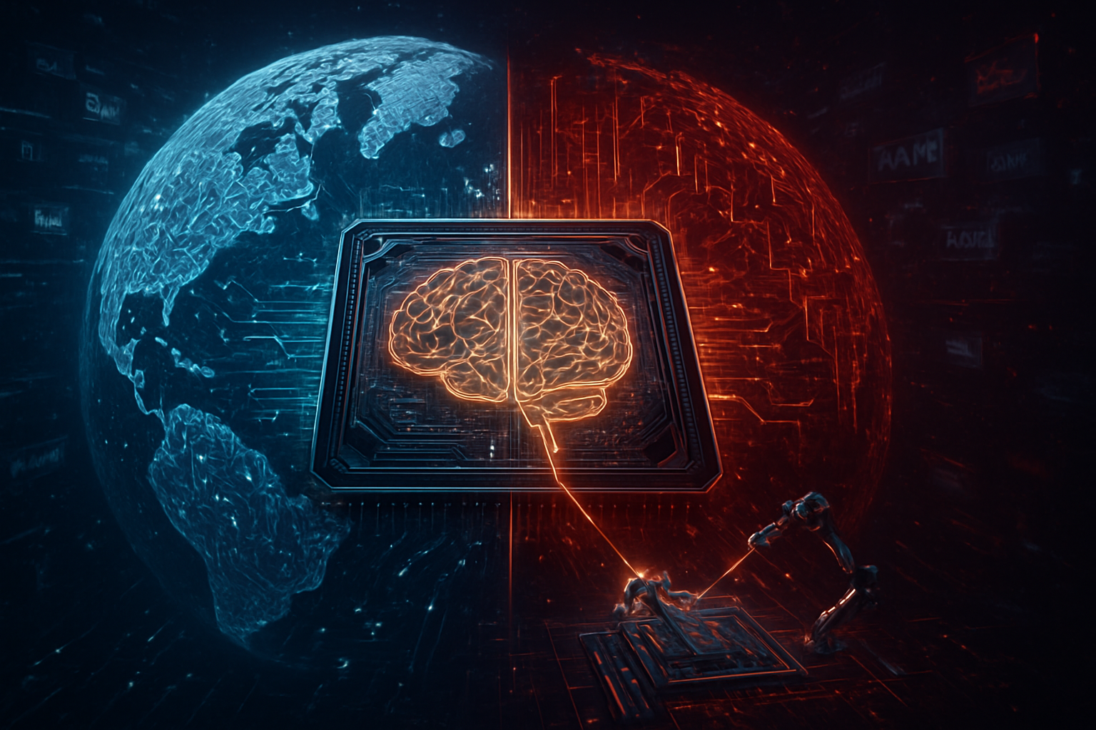
The Competitive Fallout: Tech Giants Scramble for Ground
The launch of GPT-5.2 has sent shockwaves through the industry, particularly for Alphabet Inc. (NASDAQ:GOOGL) and Meta (NASDAQ:META). While Google’s Gemini 3 briefly held the lead in late 2025, OpenAI’s 70.9% score on GDPval has forced a strategic pivot in Mountain View. Reports suggest Google is fast-tracking its "Gemini Deep Research" agents to compete with the GPT-5.2 Pro tier. Meanwhile, Microsoft (NASDAQ:MSFT), OpenAI's primary partner, has already integrated the "Thinking" tier into its 365 Copilot suite, offering enterprise customers a significant productivity advantage.
Anthropic remains a formidable specialist competitor, with its Claude 4.5 model still holding a narrow edge in software engineering benchmarks (80.9% vs GPT-5.2's 80.0%). However, OpenAI’s aggressive move to diversify into media has created a new front in the AI wars. Coinciding with the GPT-5.2 launch, OpenAI announced a $1 billion partnership with The Walt Disney Company (NYSE:DIS). This deal grants OpenAI access to vast libraries of intellectual property to train and refine AI-native video and storytelling tools, positioning GPT-5.2 as the backbone for the next generation of digital entertainment.
Solving the 'Performance Paradox' and Redefining Knowledge Work
For the past year, AI researchers have debated the "performance paradox"—the phenomenon where AI models excel in laboratory benchmarks but fail to deliver consistent value in messy, real-world business environments. OpenAI claims GPT-5.2 finally solves this by aligning its "thinking" process with human professional standards. By matching the output quality of a human expert at 11 times the speed and less than 1% of the cost, GPT-5.2 shifts the focus from raw intelligence to economic utility.
The wider significance of this milestone cannot be overstated. We are moving beyond the era of "hallucinating chatbots" into an era of "reliable agents." However, this leap brings significant concerns regarding white-collar job displacement. If a model can perform at the level of a mid-career professional in legal document analysis or financial forecasting, the entry-level "pipeline" for these professions may be permanently disrupted. This marks a major shift from previous AI milestones, like GPT-4, which were seen more as experimental tools than direct professional replacements.
The Horizon: Adult Mode and the Path to AGI
Looking ahead, the GPT-5.2 ecosystem is expected to evolve rapidly. OpenAI has confirmed that it will launch a "verified user" tier, colloquially known as "Adult Mode," in Q1 2026. Utilizing advanced AI-driven age-prediction software, this mode will loosen the strict safety filters that have historically frustrated creative writers and professionals working in mature industries. This move signals OpenAI's intent to treat its users as adults, moving away from the "nanny-bot" reputation of earlier models.
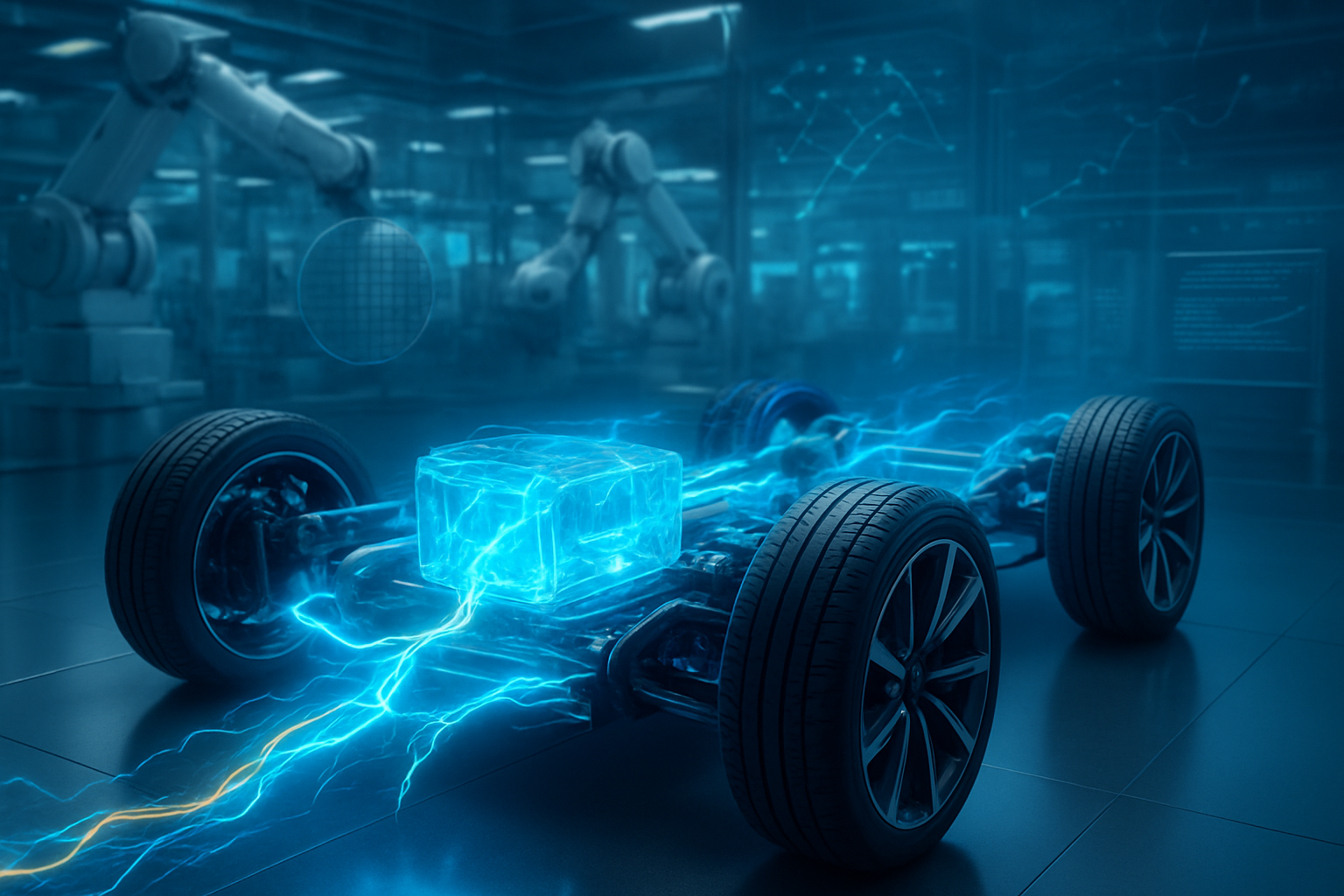
Near-term developments will likely focus on "World Models," where GPT-5.2 can simulate physical environments for robotics and industrial design. The primary challenge remaining is the massive energy consumption required to run the "Pro" tier. As NVIDIA (NASDAQ:NVDA) continues to ship the next generation of Blackwell-Ultra chips to satisfy this demand, the industry’s focus will shift toward making these "thinking" capabilities more energy-efficient and accessible to smaller developers via the OpenAI API.
A New Era for Artificial Intelligence
The launch of GPT-5.2 represents a watershed moment in the history of technology. By achieving 70.9% on the GDPval benchmark, OpenAI has effectively declared that the "performance paradox" is over. The model's ability to reason, plan, and execute tasks at a professional level—split across the Instant, Thinking, and Pro tiers—provides a blueprint for how AI will be integrated into the global economy over the next decade.
In the coming weeks, the industry will be watching closely as enterprise users begin to deploy GPT-5.2 agents at scale. The true test will not be in the benchmarks, but in the efficiency gains reported by the companies adopting this new "thinking" architecture. As we navigate the early weeks of 2026, one thing is clear: the bar for what constitutes "artificial intelligence" has been permanently raised.
This content is intended for informational purposes only and represents analysis of current AI developments.
TokenRing AI delivers enterprise-grade solutions for multi-agent AI workflow orchestration, AI-powered development tools, and seamless remote collaboration platforms.
For more information, visit https://www.tokenring.ai/.