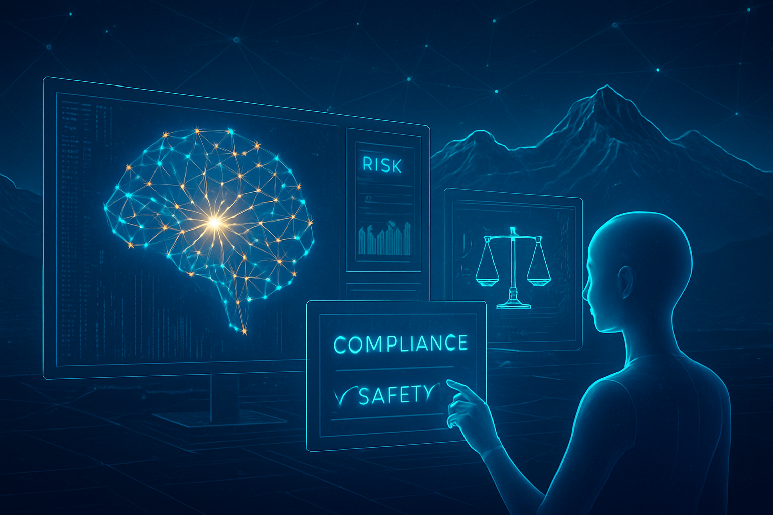
Blog

  • The Body Electric: How Dragonwing and Jetson AGX Thor Sparked the Physical AI Revolution

    The Body Electric: How Dragonwing and Jetson AGX Thor Sparked the Physical AI Revolution

    As of January 1, 2026, the artificial intelligence landscape has undergone a profound metamorphosis. The era of "Chatbot AI"—where intelligence was confined to text boxes and cloud-based image generation—has been superseded by the era of Physical AI. This shift represents the transition from digital intelligence to embodied intelligence: AI that can perceive, reason, and interact with the three-dimensional world in real-time. This revolution has been catalyzed by a new generation of "Physical AI" silicon that brings unprecedented compute power to the edge, effectively giving AI a body and a nervous system.

    The cornerstone of this movement is the arrival of ultra-high-performance, low-power chips designed specifically for autonomous machines. Leading the charge are Qualcomm’s (NASDAQ: QCOM) newly rebranded Dragonwing platform and NVIDIA’s (NASDAQ: NVDA) Jetson AGX Thor. These processors have moved the "brain" of the AI from distant data centers directly into the chassis of humanoid robots, autonomous delivery vehicles, and smart automotive cabins. By eliminating the latency of the cloud and providing the raw horsepower necessary for complex sensor fusion, these chips have turned the dream of "Edge AI" into a tangible, physical reality.

    The Silicon Architecture of Embodiment

    Technically, the leap from 2024’s edge processors to the hardware of 2026 is staggering. NVIDIA’s Jetson AGX Thor, which began shipping to developers in late 2025, is built on the Blackwell GPU architecture. It delivers a massive 2,070 FP4 TFLOPS of performance—a nearly 7.5-fold increase over its predecessor, the Jetson Orin. This level of compute is critical for "Project GR00T," NVIDIA’s foundation model for humanoid robots, allowing machines to process multimodal data from cameras, LiDAR, and force sensors simultaneously to navigate complex human environments. Thor also introduces a specialized "Holoscan Sensor Bridge," which slashes the time it takes for data to travel from a robot's "eyes" to its "brain," a necessity for safe real-time interaction.

    In contrast, Qualcomm has carved out a dominant position in industrial and enterprise applications with its Dragonwing IQ-9075 flagship. While NVIDIA focuses on raw TFLOPS for complex humanoids, Qualcomm has optimized for power efficiency and integrated connectivity. The Dragonwing platform features dual Hexagon NPUs capable of 100 INT8 TOPS, designed to run 13-billion parameter models locally while maintaining a thermal profile suitable for fanless industrial drones and Autonomous Mobile Robots (AMRs). Crucially, the IQ-9075 is the first of its kind to integrate UHF RFID, 5G, and Wi-Fi 7 directly into the SoC, allowing robots in smart warehouses to track inventory with centimeter-level precision while maintaining a constant high-speed data link.

    This new hardware differs from previous iterations by prioritizing "Sim-to-Real" capabilities. Previous edge chips were largely reactive, running simple computer vision models. Today’s Physical AI chips are designed to run "World Models"—AI that understands the laws of physics. Industry experts have noted that the ability of these chips to run local, high-fidelity simulations allows robots to "rehearse" a movement in a fraction of a second before executing it in the real world, drastically reducing the risk of accidents in shared human-robot spaces.

    A New Competitive Landscape for the AI Titans

    The emergence of Physical AI has reshaped the strategic priorities of the world’s largest tech companies. For NVIDIA, Jetson AGX Thor is the final piece of CEO Jensen Huang’s "Three-Computer" vision, positioning the company as the end-to-end provider for the robotics industry—from training in the cloud to simulation in the Omniverse and deployment at the edge. This vertical integration has forced competitors to accelerate their own hardware-software stacks. Qualcomm’s pivot to the Dragonwing brand signals a direct challenge to NVIDIA’s industrial dominance, leveraging Qualcomm’s historical strength in mobile power efficiency to capture the massive market for battery-operated edge devices.

    The impact extends deep into the automotive sector. Manufacturers like BYD (OTC: BYDDF) and Volvo (OTC: VLVLY) have already begun integrating DRIVE AGX Thor into their 2026 vehicle lineups. These chips don't just power self-driving features; they transform the automotive cabin into a "Physical AI" environment. With Dragonwing and Thor, cars can now perform real-time "cabin sensing"—detecting a driver’s fatigue level or a passenger’s medical distress—and respond with localized AI agents that don't require an internet connection to function. This has created a secondary market for "AI-first" automotive software, where startups are competing to build the most responsive and intuitive in-car assistants.

    Furthermore, the democratization of this technology is occurring through strategic partnerships. Qualcomm’s 2025 acquisition of Arduino led to the release of the Arduino Uno Q, a "dual-brain" board that pairs a Dragonwing processor with a traditional microcontroller. This move has lowered the barrier to entry for smaller robotics startups and the maker community, allowing them to build sophisticated machines that were previously the sole domain of well-funded labs. As a result, we are seeing a surge in "TinyML" applications, where ultra-low-power sensors act as a "peripheral nervous system," waking up the more powerful "central brain" (Thor or Dragonwing) only when complex reasoning is required.

    The Broader Significance: AI Gets a Sense of Self

    The rise of Physical AI marks a departure from the "Stochastic Parrot" era of AI. When an AI is embodied in a robot powered by a Jetson AGX Thor, it is no longer just predicting the next word in a sentence; it is predicting the next state of the physical world. This has profound implications for AI safety and reliability. Because these machines operate at the edge, they are not subject to the "hallucinations" caused by cloud latency or connectivity drops. The intelligence is local, grounded in the immediate physical context of the machine, which is a prerequisite for deploying AI in high-stakes environments like surgical suites or nuclear decommissioning sites.

    However, this shift also brings new concerns, particularly regarding privacy and security. With machines capable of processing high-resolution video and sensor data locally, the "Edge AI" promise of privacy is put to the test. While data doesn't necessarily leave the device, the sheer amount of information these machines "see" is unprecedented. Regulators are already grappling with how to categorize "Physical AI" entities—are they tools, or are they a new class of autonomous agents? The comparison to previous milestones, like the release of GPT-4, is clear: while LLMs changed how we write and code, Physical AI is changing how we build and move.

    The transition to Physical AI also represents the ultimate realization of TinyML. By moving the most critical inference tasks to the very edge of the network, the industry is reducing its reliance on massive, energy-hungry data centers. This "distributed intelligence" model is seen as a more sustainable path for the future of AI, as it leverages the efficiency of specialized silicon like the Dragonwing series to perform tasks that would otherwise require kilowatts of power in a server farm.

    The Horizon: From Factories to Front Porches

    Looking ahead to the remainder of 2026 and beyond, we expect to see Physical AI move from industrial settings into the domestic sphere. Near-term developments will likely focus on "General Purpose Humanoids" capable of performing unstructured tasks in the home, such as folding laundry or organizing a kitchen. These applications will require even further refinements in "Sim-to-Real" technology, where AI models can generalize from virtual training to the messy, unpredictable reality of a human household.

    The next great challenge for the industry will be the "Battery Barrier." While chips like the Dragonwing IQ-9075 have made great strides in efficiency, the mechanical actuators of robots remain power-hungry. Experts predict that the next breakthrough in Physical AI will not be in the "brain" (the silicon), but in the "muscles"—new types of high-efficiency electric motors and solid-state batteries designed specifically for the robotics form factor. Once the power-to-weight ratio of these machines improves, we may see the first truly ubiquitous personal robots.

    A New Chapter in the History of Intelligence

    The "Edge AI Revolution" of 2025 and 2026 will likely be remembered as the moment AI became a participant in our world rather than just an observer. The release of NVIDIA’s Jetson AGX Thor and Qualcomm’s Dragonwing platform provided the necessary "biological" leap in compute density to make embodied intelligence possible. We have moved beyond the limits of the screen and entered an era where intelligence is woven into the very fabric of our physical environment.

    As we move forward, the key metric for AI success will no longer be "parameters" or "pre-training data," but "physical agency"—the ability of a machine to safely and effectively navigate the complexities of the real world. In the coming months, watch for the first large-scale deployments of Thor-powered humanoids in logistics hubs and the integration of Dragonwing-based "smart city" sensors that can manage traffic and emergency responses in real-time. The revolution is no longer coming; it is already here, and it has a body.


    This content is intended for informational purposes only and represents analysis of current AI developments.

    TokenRing AI delivers enterprise-grade solutions for multi-agent AI workflow orchestration, AI-powered development tools, and seamless remote collaboration platforms.
    For more information, visit https://www.tokenring.ai/.

  • The Great Decoupling: How Hyperscaler Custom Silicon is Ending NVIDIA’s AI Monopoly

    The Great Decoupling: How Hyperscaler Custom Silicon is Ending NVIDIA’s AI Monopoly

    The artificial intelligence industry has reached a historic inflection point as of early 2026, marking the beginning of what analysts call the "Great Decoupling." For years, the tech world was beholden to the supply chains and pricing power of NVIDIA Corporation (NASDAQ: NVDA), whose H100 and Blackwell GPUs became the de facto currency of the generative AI era. However, the tide has turned. As the industry shifts its focus from training massive foundation models to the high-volume, cost-sensitive world of inference, the world’s largest hyperscalers—Google, Amazon, and Meta—have finally unleashed their secret weapons: custom-built AI accelerators designed to bypass the "NVIDIA tax."

    Leading this charge is the general availability of Alphabet Inc.’s (NASDAQ: GOOGL) TPU v7, codenamed "Ironwood." Alongside the deployment of Amazon.com, Inc.’s (NASDAQ: AMZN) Trainium 3 and Meta Platforms, Inc.’s (NASDAQ: META) MTIA v3, these chips represent a fundamental shift in the AI power dynamic. No longer content to be just NVIDIA’s biggest customers, these tech giants are vertically integrating their hardware and software stacks to achieve "silicon sovereignty," promising to slash AI operating costs and redefine the competitive landscape for the next decade.

    The Ironwood Era: Inside Google’s TPU v7 Breakthrough

    Google’s TPU v7 "Ironwood," which entered general availability in late 2025, represents the most significant architectural overhaul in the Tensor Processing Unit's decade-long history. Built on a cutting-edge 3nm process node, Ironwood delivers a staggering 4.6 PFLOPS of dense FP8 compute per chip—an 11x increase over the TPU v5p. More importantly, it features 192GB of HBM3e memory with a bandwidth of 7.4 TB/s, specifically engineered to handle the massive KV-caches required for the latest trillion-parameter frontier models like Gemini 2.0 and the upcoming Gemini 3.0.

    What truly sets Ironwood apart from NVIDIA’s Blackwell architecture is its networking philosophy. While NVIDIA relies on NVLink to cluster GPUs in relatively small pods, Google has refined its proprietary Optical Circuit Switch (OCS) and 3D Torus topology. A single Ironwood "Superpod" can connect 9,216 chips into a unified compute domain, providing an aggregate of 42.5 ExaFLOPS of FP8 compute. This allows Google to treat thousands of chips as a single "brain," drastically reducing the latency and networking overhead that typically plagues large-scale distributed inference.

    Initial reactions from the AI research community have been overwhelmingly positive, particularly regarding the TPU’s energy efficiency. Experts at the AI Hardware Summit noted that while NVIDIA’s B200 remains a powerhouse for raw training, Ironwood offers nearly double the performance-per-watt for inference tasks. This efficiency is a direct result of Google’s ASIC approach: by stripping away the legacy graphics circuitry found in general-purpose GPUs, Google has created a "lean and mean" machine dedicated solely to the matrix multiplications that power modern transformers.

    The Cloud Counter-Strike: AWS and Meta’s Silicon Sovereignty

    Not to be outdone, Amazon.com, Inc. (NASDAQ: AMZN) has accelerated its custom silicon roadmap with the full deployment of Trainium 3 (Trn3) in early 2026. Manufactured on TSMC’s 3nm node, Trn3 marks a strategic pivot for AWS: the convergence of its training and inference lines. Amazon has realized that the "thinking" models of 2026, such as Anthropic’s Claude 4 and Amazon’s own Nova series, require the massive memory and FLOPS previously reserved for training. Trn3 delivers 2.52 PFLOPS of FP8 compute, offering a 50% better price-performance ratio than the equivalent NVIDIA H100 or B200 instances currently available on the market.

    Meta Platforms, Inc. (NASDAQ: META) is also making massive strides with its MTIA v3 (Meta Training and Inference Accelerator). While Meta remains one of NVIDIA’s largest customers for the raw training of its Llama family, the company has begun migrating its massive recommendation engines—the heart of Facebook and Instagram—to its own silicon. MTIA v3 features a significant upgrade to HBM3e memory, allowing Meta to serve Llama 4 models to billions of users with a fraction of the power consumption required by off-the-shelf GPUs. This move toward infrastructure autonomy is expected to save Meta billions in capital expenditures over the next three years.

    Even Microsoft Corporation (NASDAQ: MSFT) has joined the fray with the volume rollout of its Maia 200 (Braga) chips. Designed to reduce the "Copilot tax" for Azure OpenAI services, Maia 200 is now powering a significant portion of ChatGPT’s inference workloads. This collective push by the hyperscalers has created a multi-polar hardware ecosystem where the choice of chip is increasingly dictated by the specific model architecture and the desired cost-per-token, rather than brand loyalty to NVIDIA.

    Breaking the CUDA Moat: The Software Revolution

    The primary barrier to decoupling has always been NVIDIA’s proprietary CUDA software ecosystem. However, in 2026, that moat is being bridged by a maturing open-source software stack. OpenAI’s Triton has emerged as the industry’s primary "off-ramp," allowing developers to write high-performance kernels in Python that are hardware-agnostic. Triton now features mature backends for Google’s TPU, AWS Trainium, and even AMD’s MI350 series, effectively neutralizing the software advantage that once made NVIDIA GPUs indispensable.

    Furthermore, the integration of PyTorch 2.x and the upcoming 3.0 release has solidified torch.compile as the standard for AI development. By using the OpenXLA (Accelerated Linear Algebra) compiler and the PJRT interface, PyTorch can now automatically optimize models for different hardware backends with minimal performance loss. This means a developer can train a model on an NVIDIA-based workstation and deploy it to a Google TPU v7 or an AWS Trainium 3 cluster with just a few lines of code.

    This software abstraction has profound implications for the market. It allows AI labs and startups to build "Agentlakes"—composable architectures that can dynamically shift workloads between different cloud providers based on real-time pricing and availability. The "NVIDIA tax"—the 70-80% margins the company once commanded—is being eroded as hyperscalers use their own silicon to offer AI services at lower price points, forcing a competitive race to the bottom in the inference market.

    The Future of Distributed Compute: 2nm and Beyond

    Looking ahead to late 2026 and 2027, the battle for silicon supremacy will move to the 2nm process node. Industry insiders predict that the next generation of chips will focus heavily on "Interconnect Fusion." NVIDIA is already fighting back with its NVLink Fusion technology, which aims to open its high-speed interconnects to third-party ASICs, attempting to move the lock-in from the chip level to the network level. Meanwhile, Google is rumored to be working on TPU v8, which may feature integrated photonic interconnects directly on the die to eliminate electronic bottlenecks entirely.

    The next frontier will also involve "Edge-to-Cloud" continuity. As models become more modular through techniques like Mixture-of-Experts (MoE), we expect to see hybrid inference strategies where the "base" of a model runs on energy-efficient custom silicon in the cloud, while specialized "expert" modules run locally on 2nm-powered mobile devices and PCs. This would create a truly distributed AI fabric, further reducing the reliance on massive centralized GPU clusters.

    However, challenges remain. The fragmentation of the hardware landscape could lead to a "optimization tax," where developers spend more time tuning models for different architectures than they do on actual research. Additionally, the massive capital requirements for 2nm fabrication mean that only the largest hyperscalers can afford to play this game, potentially leading to a new form of "Cloud Oligarchy" where smaller players are priced out of the custom silicon race.

    Conclusion: A New Era of AI Economics

    The "Great Decoupling" of 2026 marks the end of the monolithic GPU era and the birth of a more diverse, efficient, and competitive AI hardware ecosystem. While NVIDIA remains a dominant force in high-end research and frontier model training, the rise of Google’s TPU v7 Ironwood, AWS Trainium 3, and Meta’s MTIA v3 has proven that the world’s biggest tech companies are no longer willing to outsource their infrastructure's future.

    The key takeaway for the industry is that AI is transitioning from a scarcity-driven "gold rush" to a cost-driven "utility phase." In this new world, "Silicon Sovereignty" is the ultimate strategic advantage. As we move into the second half of 2026, the industry will be watching closely to see how NVIDIA responds to this erosion of its moat and whether the open-source software stack can truly maintain parity across such a diverse range of hardware. One thing is certain: the era of the $40,000 general-purpose GPU as the only path to AI success is officially over.


    This content is intended for informational purposes only and represents analysis of current AI developments.

    TokenRing AI delivers enterprise-grade solutions for multi-agent AI workflow orchestration, AI-powered development tools, and seamless remote collaboration platforms.
    For more information, visit https://www.tokenring.ai/.

  • Texas Instruments Ignites the Reshoring Revolution: SM1 Fab in Sherman Begins Production of AI and Automotive Silicon

    Texas Instruments Ignites the Reshoring Revolution: SM1 Fab in Sherman Begins Production of AI and Automotive Silicon

    On December 17, 2025, the landscape of American semiconductor manufacturing shifted as Texas Instruments (NASDAQ: TXN) officially commenced production at its SM1 fab in Sherman, Texas. This milestone marks the first of four planned facilities at the site, representing a massive $30 billion investment aimed at securing the foundational silicon supply chain. As of January 1, 2026, the facility is actively ramping up its output, signaling a pivotal moment in the "Global Reshoring Boom" that seeks to return high-tech manufacturing to U.S. soil.

    The opening of SM1 is not merely a corporate expansion; it is a strategic maneuver to provide the essential components that power the modern world. While much of the public's attention remains fixed on high-end logic processors, the Sherman facility focuses on the "foundational" chips—analog and embedded processors—that are the unsung heroes of the AI revolution and the automotive industry’s transition to electrification. By internalizing its supply chain, Texas Instruments is positioning itself as a cornerstone of industrial stability in an increasingly volatile global market.

    Technical Specifications and the 300mm Advantage

    The SM1 facility is a marvel of modern engineering, specifically designed to produce 300mm (12-inch) wafers. This transition from the industry-standard 200mm wafers is a game-changer for Texas Instruments, providing 2.3 times more surface area per wafer. This shift is expected to yield an estimated 40% reduction in chip-level fabrication costs, allowing the company to maintain high margins while providing competitive pricing for the massive volumes required by the AI and automotive sectors.

    Unlike the sub-5nm "bleeding edge" nodes used for CPUs and GPUs, the Sherman site operates primarily in the 28nm to 130nm range. These "mature" nodes are the sweet spot for high-performance analog and embedded processing. These chips are designed for durability, high-voltage precision, and thermal stability—qualities essential for power management in AI data centers and battery management systems in electric vehicles (EVs). Initial reactions from industry experts suggest that TI's focus on these foundational nodes is a masterstroke, addressing the specific types of chip shortages that paralyzed the global economy in the early 2020s.

    The facility’s output includes advanced multiphase controllers and smart power stages. These components are critical for the 800VDC architectures now becoming standard in AI data centers, where they manage the intense power delivery required by high-performance AI accelerators. Furthermore, the fab is producing the latest Sitara™ AM69A processors, which are optimized for "Edge AI" applications, enabling autonomous robots and smart vehicles to perform complex computer vision tasks with minimal power consumption.

    Market Impact: Powering the AI Giants and Automakers

    The start of production at SM1 has immediate implications for tech giants and AI startups alike. As companies like NVIDIA (NASDAQ: NVDA) and Advanced Micro Devices (NASDAQ: AMD) push the limits of compute power, they require an equally sophisticated "nervous system" of power management and signal chain components to keep their chips running. Texas Instruments is now positioned to be the primary domestic supplier of these components, offering a "geopolitically dependable" supply chain that mitigates the risks associated with overseas foundries.

    For the automotive sector, the Sherman fab is a lifeline. Major U.S. automakers, including Ford (NYSE: F) and Tesla (NASDAQ: TSLA), stand to benefit from a localized supply of chips used in battery management, advanced driver-assistance systems (ADAS), and vehicle-to-everything (V2X) communication. By manufacturing these chips in Texas, TI reduces lead times and provides a buffer against the supply shocks that have historically disrupted vehicle production lines.

    This move also places significant pressure on international competitors like Infineon and Analog Devices (NASDAQ: ADI). By aiming to manufacture more than 95% of its chips internally by 2030, Texas Instruments is aggressively decoupling from external foundries. This vertical integration provides a strategic advantage in terms of cost control and quality assurance, potentially allowing TI to capture a larger share of the industrial and automotive markets as they continue to digitize and electrify.

    The Global Reshoring Boom and Geopolitical Stability

    The Sherman mega-site is a flagship project of the broader U.S. effort to reclaim semiconductor sovereignty. Supported by $1.6 billion in direct funding from the CHIPS and Science Act, as well as billions more in investment tax credits, the project is a testament to the success of federal incentives in driving domestic manufacturing. This "Global Reshoring Boom" is a response to the vulnerabilities exposed by the global pandemic and rising geopolitical tensions, which highlighted the danger of over-reliance on a few concentrated manufacturing hubs in East Asia.

    In the broader AI landscape, the SM1 fab represents the "infrastructure layer" that makes large-scale AI deployment possible. While software breakthroughs often grab the headlines, those breakthroughs cannot be realized without the physical hardware to support them. TI’s investment ensures that as AI moves from experimental labs into every facet of the industrial and consumer world, the foundational hardware will be available and sustainably sourced.

    However, the rapid expansion of such massive facilities also brings concerns regarding resource consumption and labor. The Sherman site is expected to support 3,000 direct jobs, but the demand for highly skilled technicians and engineers remains a challenge for the North Texas region. Furthermore, the environmental impact of large-scale semiconductor fabrication—specifically water and energy usage—remains a point of scrutiny, though TI has committed to utilizing advanced recycling and sustainable building practices for the Sherman campus.

    The Road to 100 Million Chips Per Day

    Looking ahead, the opening of SM1 is only the beginning. The exterior shell for the second fab, SM2, is already complete, with cleanroom installation and tool positioning scheduled to begin later in 2026. Two additional fabs, SM3 and SM4, are planned for future phases, with the ultimate goal of producing over 100 million chips per day at the Sherman site alone. This roadmap suggests that Texas Instruments is betting heavily on a long-term, sustained demand for foundational silicon.

    In the near term, we can expect to see TI release a new generation of "intelligent" analog chips that integrate more AI-driven monitoring and self-diagnostic features directly into the hardware. These will be crucial for the next generation of smart grids, medical devices, and industrial automation. Experts predict that the Sherman site will become the epicenter of a new "Silicon Prairie," attracting a cluster of satellite industries and suppliers to North Texas.

    The challenge for TI will be maintaining this momentum as global economic conditions fluctuate. While the current demand for AI and EV silicon is high, the semiconductor industry is notoriously cyclical. However, by focusing on the foundational chips that are required regardless of which specific AI model or vehicle brand wins the market, TI has built a resilient business model that is well-positioned for the decades to come.

    A New Era for American Silicon

    The commencement of production at Texas Instruments' SM1 fab is a landmark achievement in the history of American technology. It signifies a shift away from the "fab-lite" models of the past two decades and a return to the era of the integrated device manufacturer. By combining cutting-edge 300mm fabrication with a strategic focus on the essential components of the modern economy, TI is not just building chips; it is building a foundation for the next century of innovation.

    As we move further into 2026, the success of the Sherman site will be a bellwether for the success of the CHIPS Act and the broader reshoring movement. The ability to produce 100 million chips a day domestically would be a transformative shift in the global supply chain, providing the stability and scale needed to fuel the AI-driven future. For now, the lights are on in Sherman, and the first wafers are rolling off the line—a clear signal that the American semiconductor industry is back in the driver's seat.


    This content is intended for informational purposes only and represents analysis of current AI developments.

    TokenRing AI delivers enterprise-grade solutions for multi-agent AI workflow orchestration, AI-powered development tools, and seamless remote collaboration platforms.
    For more information, visit https://www.tokenring.ai/.

  • The High-Bandwidth Memory Arms Race: HBM4 and the Quest for Trillion-Parameter AI Supremacy

    The High-Bandwidth Memory Arms Race: HBM4 and the Quest for Trillion-Parameter AI Supremacy

    As of January 1, 2026, the artificial intelligence industry has reached a critical hardware inflection point. The transition from the HBM3E era to the HBM4 generation is no longer a roadmap projection but a high-stakes reality. Driven by the voracious memory requirements of 100-trillion parameter AI models, the "Big Three" memory makers—Samsung Electronics (KRX: 005930), SK Hynix (KRX: 000660), and Micron Technology (NASDAQ: MU)—are locked in a fierce capacity race to supply the next generation of AI accelerators.

    This shift represents more than just a speed bump; it is a fundamental architectural change. With NVIDIA (NASDAQ: NVDA) and Advanced Micro Devices (NASDAQ: AMD) rolling out their most ambitious chips to date, the availability of HBM4 has become the primary bottleneck for AI progress. The ability to house entire massive language models within active memory is the new frontier, and the early winners of 2026 are those who can master the complex physics of 12-layer and 16-layer HBM4 stacking.

    The HBM4 Breakthrough: Doubling the Data Highway

    The defining characteristic of HBM4 is the doubling of the memory interface width from 1024-bit to 2048-bit. This "GPT-4 moment" for hardware allows for a massive leap in data throughput without the exponential power consumption increases that plagued late-stage HBM3E. Current 2026 specifications show HBM4 stacks reaching bandwidths between 2.0 TB/s and 2.8 TB/s per stack. Samsung has taken an early lead in volume, having secured Production Readiness Approval (PRA) from NVIDIA in late 2025 and commencing mass production of 12-Hi (12-layer) HBM4 at its Pyeongtaek facility this month.

    Technically, HBM4 introduces hybrid bonding and custom logic dies, moving away from the traditional micro-bump interface. This allows for a thinner profile and better thermal management, which is essential as GPUs now regularly exceed 1,000 watts of power draw. SK Hynix, which dominated the HBM3E cycle, has shifted its strategy to a "One-Team" alliance with Taiwan Semiconductor Manufacturing Company (NYSE: TSM), utilizing TSMC’s 5nm and 3nm nodes for the base logic dies. This collaboration aims to provide a more "system-level" memory solution, though their full-scale volume ramp is not expected until the second quarter of 2026.

    Initial reactions from the AI research community have been overwhelmingly positive, as the increased memory capacity directly translates to lower latency in inference. Experts at leading AI labs note that HBM4 is the first memory technology designed specifically for the "post-transformer" era, where the "memory wall"—the gap between processor speed and memory access—has been the single greatest hurdle to achieving real-time reasoning in models exceeding 50 trillion parameters.

    The Strategic Battle: Samsung’s Resurgence and the SK Hynix-TSMC Alliance

    The competitive landscape has shifted dramatically in early 2026. Samsung, which struggled to gain traction during the HBM3E transition, has leveraged its position as an integrated device manufacturer (IDM). By handling memory production, logic die design, and advanced packaging internally, Samsung has offered a "turnkey" HBM4 solution that has proven attractive to NVIDIA for its new Rubin R100 platform. This vertical integration has allowed Samsung to reclaim significant market share that it had previously lost to SK Hynix.

    Meanwhile, Micron Technology has carved out a niche as the performance leader. In early January 2026, Micron confirmed that its entire HBM4 production capacity for the year is already sold out, largely due to massive pre-orders from hyperscalers like Microsoft and Google. Micron’s 1β (1-beta) DRAM process has allowed it to achieve 2.8 TB/s speeds, slightly edging out the standard JEDEC specifications and making its stacks the preferred choice for high-frequency trading and specialized scientific research clusters.

    The implications for AI labs are profound. The scarcity of HBM4 means that only the most well-funded organizations will have access to the hardware necessary to train 100-trillion parameter models in a reasonable timeframe. This reinforces the "compute moat" held by tech giants, as the cost of a single HBM4-equipped GPU node is expected to rise by 30% compared to the previous generation. However, the increased efficiency of HBM4 may eventually lower the total cost of ownership by reducing the number of nodes required to maintain the same level of performance.

    Breaking the Memory Wall: Scaling to 100-Trillion Parameters

    The HBM4 capacity race is fundamentally about the feasibility of the next generation of AI. As we move into 2026, the industry is no longer satisfied with 1.8-trillion parameter models like GPT-4. The goal is now 100 trillion parameters—a scale that mimics the complexity of the human brain's synaptic connections. Such models require multi-terabyte memory pools just to store their weights. Without HBM4’s 2048-bit interface and 64GB-per-stack capacity, these models would be forced to rely on slower inter-chip communication, leading to "stuttering" in AI reasoning.

    Compared to previous milestones, such as the introduction of HBM2 or HBM3, the move to HBM4 is seen as a more significant structural shift. It marks the first time that memory manufacturers are becoming "co-designers" of the AI processor. The use of custom logic dies means that the memory is no longer a passive storage bin but an active participant in data pre-processing. This helps address the "thermal ceiling" that threatened to stall GPU development in 2024 and 2025.

    However, concerns remain regarding the environmental impact and supply chain fragility. The manufacturing process for HBM4 is significantly more complex and has lower yields than standard DDR5 memory. This has led to a "bifurcation" of the semiconductor market, where resources are being diverted away from consumer electronics to feed the AI beast. Analysts warn that any disruption in the supply of high-purity chemicals or specialized packaging equipment could halt the production of HBM4, potentially causing a global "AI winter" driven by hardware shortages rather than a lack of algorithmic progress.

    Beyond HBM4: The Roadmap to HBM5 and "Feynman" Architectures

    Even as HBM4 begins its mass-market rollout, the industry is already looking toward HBM5. SK Hynix recently unveiled its 2029-2031 roadmap, confirming that HBM5 has moved into the formal design phase. Expected to debut around 2028, HBM5 is projected to feature a 4096-bit interface—doubling the width again—and utilize "bumpless" copper-to-copper direct bonding. This will likely support NVIDIA’s rumored "Feynman" architecture, which aims for a 10x increase in compute density over the current Rubin platform.

    In the near term, 2027 will likely see the introduction of HBM4E (Extended), which will push stack heights to 16-Hi and 20-Hi. This will enable a single GPU to carry over 1TB of high-bandwidth memory. Such a development would allow for "edge AI" servers to run massive models locally, potentially solving many of the privacy and latency issues currently associated with cloud-based AI.

    The challenge moving forward will be cooling. As memory stacks get taller and more dense, the heat generated in the middle of the stack becomes difficult to dissipate. Experts predict that 2026 and 2027 will see a surge in liquid-to-chip cooling adoption in data centers to accommodate these HBM4-heavy systems. The "memory-centric" era of computing is here, and the innovations in HBM5 will likely focus as much on thermal physics as on electrical engineering.

    A New Era of Compute: Final Thoughts

    The HBM4 capacity race of 2026 marks the end of general-purpose hardware dominance in the data center. We have entered an era where memory is the primary differentiator of AI capability. Samsung’s aggressive return to form, SK Hynix’s strategic alliance with TSMC, and Micron’s sold-out performance lead all point to a market that is maturing but remains incredibly volatile.

    In the history of AI, the HBM4 transition will likely be remembered as the moment when hardware finally caught up to the ambitions of software architects. It provides the necessary foundation for the 100-trillion parameter models that will define the latter half of this decade. For the tech industry, the key takeaway is clear: the "Memory Wall" has not been demolished, but HBM4 has built a massive, high-speed bridge over it.

    In the coming weeks and months, the industry will be watching the initial benchmarks of the NVIDIA Rubin R100 and the AMD Instinct MI400. These results will reveal which memory partner—Samsung, SK Hynix, or Micron—has delivered the best real-world performance. As 2026 unfolds, the success of these hardware platforms will determine the pace at which artificial general intelligence (AGI) moves from a theoretical goal to a practical reality.


    This content is intended for informational purposes only and represents analysis of current AI developments.

    TokenRing AI delivers enterprise-grade solutions for multi-agent AI workflow orchestration, AI-powered development tools, and seamless remote collaboration platforms.
    For more information, visit https://www.tokenring.ai/.

  • Intel Reclaims the Silicon Throne: 18A Hits High-Volume Production as 14A PDKs Reach Global Customers

    Intel Reclaims the Silicon Throne: 18A Hits High-Volume Production as 14A PDKs Reach Global Customers

    In a landmark moment for the semiconductor industry, Intel Corporation (NASDAQ:INTC) has officially announced that its cutting-edge 18A (1.8nm-class) manufacturing node has entered high-volume manufacturing (HVM). This achievement marks the successful completion of CEO Pat Gelsinger’s ambitious "five nodes in four years" (5N4Y) strategy, positioning the company at the forefront of the global race for transistor density and energy efficiency. As of January 1, 2026, the first consumer and enterprise chips built on this process—codenamed Panther Lake and Clearwater Forest—are beginning to reach the market, signaling a new era for AI-driven computing.

    The announcement is further bolstered by the release of Process Design Kits (PDKs) for Intel’s next-generation 14A node to external foundry customers. By sharing these 1.4nm-class tools, Intel is effectively inviting the world’s most advanced chip designers to begin building the future of US-based manufacturing. This progress is not merely a corporate milestone; it represents a fundamental shift in the technological landscape, as Intel leverages its first-mover advantage in backside power delivery and gate-all-around (GAA) transistor architectures to challenge the dominance of rivals like TSMC (NYSE:TSM) and Samsung (KRX:005930).

    The Architecture of Leadership: RibbonFET, PowerVia, and the 18A-PT Breakthrough

    At the heart of Intel’s 18A node are two revolutionary technologies: RibbonFET and PowerVia. RibbonFET is Intel’s implementation of GAA transistors, which replace the long-standing FinFET design to provide better control over the electrical current, reducing leakage and increasing performance. While Samsung was the first to introduce GAA at the 3nm level, Intel’s 18A is the first to pair it with PowerVia—the industry's first functional backside power delivery system. By moving the power delivery circuitry to the back of the silicon wafer, Intel has eliminated the "wiring congestion" that has plagued chip design for decades. This allows for a 5% to 10% increase in logic density and significantly improved power efficiency, a critical factor for the massive power requirements of modern AI data centers.

    Intel has also introduced a specialized variant known as 18A-PT (Performance-Tuned). This node is specifically optimized for 3D-integrated circuits (3D IC) and features Foveros Direct 3D hybrid bonding. By reducing the vertical interconnect pitch to less than 5 microns, 18A-PT allows for the seamless stacking of compute dies, such as a 14A processor sitting directly atop an 18A-PT base die. This modular approach to chip design is expected to become the industry standard for high-performance AI accelerators, where memory and compute must be physically closer than ever before to minimize latency.

    The technical community has responded with cautious optimism. While early yields for 18A were reported in the 55%–65% range throughout late 2025, the trajectory suggests that Intel will reach commercial-grade maturity by mid-2026. Industry experts note that Intel’s lead in backside power delivery gives them a roughly 18-month headstart over TSMC’s N2P node, which is not expected to integrate similar technology until later this year. This "technological leapfrogging" has placed Intel in a unique position where it is no longer just catching up, but actively setting the pace for the 2nm transition.

    The Foundry War: Microsoft, AWS, and the Battle for AI Supremacy

    The success of 18A and the early rollout of 14A PDKs have profound implications for the competitive landscape of the tech industry. Microsoft (NASDAQ:MSFT) has emerged as a primary "anchor customer" for Intel Foundry, utilizing the 18A node for its Maia AI accelerators. Similarly, Amazon (NASDAQ:AMZN) has signed a multi-billion dollar agreement to produce custom AWS silicon on Intel's advanced nodes. For these tech giants, the ability to source high-end chips from US-based facilities provides a critical hedge against geopolitical instability in the Taiwan Strait, where the majority of the world's advanced logic chips are currently produced.

    For startups and smaller AI labs, the availability of 14A PDKs opens the door to "next-gen" performance that was previously the exclusive domain of companies with deep ties to TSMC. Intel’s aggressive push into the foundry business is disrupting the status quo, forcing TSMC and Samsung to accelerate their own roadmaps. As Intel begins to offer its 14A node—the first in the industry to utilize High-NA (Numerical Aperture) EUV lithography—it is positioning itself as the premier destination for companies building the next generation of Large Language Models (LLMs) and autonomous systems that require unprecedented compute density.

    The strategic advantage for Intel lies in its "systems foundry" approach. Unlike traditional foundries that only manufacture wafers, Intel is offering a full stack of services including advanced packaging (Foveros), standardized chiplet interfaces, and software optimizations. This allows customers like Broadcom (NASDAQ:AVGO) and Ericsson to design complex, multi-die systems that are more efficient than traditional monolithic chips. By securing these high-profile partners, Intel is validating its business model and proving that it can compete on both technology and service.

    A Geopolitical and Technological Pivot: The 2nm Milestone

    The transition to the 2nm class (18A) and beyond (14A) is more than just a shrinking of transistors; it is a critical component of the global AI arms race. As AI models grow in complexity, the demand for "sovereign AI" and domestic manufacturing capabilities has skyrocketed. Intel’s progress is a major win for the US Department of Defense and the RAMP-C program, which seeks to ensure that the most advanced chips for national security are built on American soil. This shift reduces the "single point of failure" risk inherent in the global semiconductor supply chain.

    Comparing this to previous milestones, the 18A launch is being viewed as Intel's "Pentium moment" or its return to the "Tick-Tock" cadence that defined its dominance in the 2000s. However, the stakes are higher now. The integration of High-NA EUV in the 14A node represents the most significant change in lithography in over a decade. While there are concerns regarding the astronomical costs of these machines—each costing upwards of $350 million—Intel’s early adoption gives it a learning curve advantage that rivals may struggle to close.

    The broader AI landscape will feel the effects of this progress through more efficient edge devices. With 18A-powered laptops and smartphones hitting the market in 2026, "Local AI" will become a reality, allowing complex generative AI tasks to be performed on-device without relying on the cloud. This has the potential to address privacy concerns and reduce the carbon footprint of AI, though it also raises new challenges regarding hardware obsolescence and the rapid pace of technological turnover.

    Looking Ahead: The Road to 14A and the High-NA Era

    As we look toward the remainder of 2026 and into 2027, the focus will shift from 18A's ramp-up to the risk production of 14A. This node will introduce "PowerDirect," Intel’s second-generation backside power delivery system, which promises even lower resistance and higher performance-per-watt. The industry is closely watching Intel's Oregon and Arizona fabs to see if they can maintain the yield improvements necessary to make 14A a commercial success.

    The near-term roadmap also includes the release of 18A-P, a performance-enhanced version of the current flagship node, slated for late 2026. This will likely serve as the foundation for the next generation of high-end gaming GPUs and AI workstations. Challenges remain, particularly in the realm of thermal management as power density continues to rise, and the industry will need to innovate new cooling solutions to keep up with these 1.4nm-class chips.

    Experts predict that by 2028, the "foundry landscape" will look entirely different, with Intel potentially holding a significant share of the external manufacturing market. The success of 14A will be the ultimate litmus test for whether Intel can truly sustain its lead. If the company can deliver on its promise of High-NA EUV production, it may well secure its position as the world's most advanced semiconductor manufacturer for the next decade.

    Conclusion: The New Silicon Standard

    Intel’s successful execution of its 18A and 14A roadmap is a defining chapter in the history of the semiconductor industry. By delivering on the "5 Nodes in 4 Years" promise, the company has silenced many of its skeptics and demonstrated a level of technical agility that few thought possible just a few years ago. The combination of RibbonFET, PowerVia, and the early adoption of High-NA EUV has created a formidable technological moat that positions Intel as a leader in the AI era.

    The significance of this development cannot be overstated; it marks the return of leading-edge manufacturing to the United States and provides the hardware foundation necessary for the next leap in artificial intelligence. As 18A chips begin to power the world’s data centers and personal devices, the industry will be watching closely for the first 14A test chips. For now, Intel has proven that it is back in the game, and the race for the sub-1nm frontier has officially begun.


    This content is intended for informational purposes only and represents analysis of current AI developments.

    TokenRing AI delivers enterprise-grade solutions for multi-agent AI workflow orchestration, AI-powered development tools, and seamless remote collaboration platforms.
    For more information, visit https://www.tokenring.ai/.

  • The Nexperia Standoff: How Europe’s Seizure of a Chip Giant Triggered a Global Supply Chain Crisis

    The Nexperia Standoff: How Europe’s Seizure of a Chip Giant Triggered a Global Supply Chain Crisis

    In a move that has sent shockwaves through the global semiconductor industry, the Dutch government has officially invoked emergency powers to seize governance control of Nexperia, the Netherlands-based chipmaker owned by China’s Wingtech Technology (SSE: 600745). This unprecedented intervention, executed under the Goods Availability Act (Wbg) in late 2025, marks a definitive end to the era of "business as usual" for foreign investment in European technology. The seizure is not merely a local regulatory hurdle but a tectonic shift in the "Global Reshoring Boom," as Western nations move to insulate their critical infrastructure from geopolitical volatility.

    The immediate significance of this development cannot be overstated. By removing Wingtech’s chairman, Zhang Xuezheng, from his role as CEO and installing government-appointed oversight, the Netherlands has effectively nationalized the strategic direction of a company that serves as the "workhorse" of the global automotive and industrial sectors. While Nexperia does not produce the high-end 2nm processors found in flagship AI servers, its dominance in "foundational" semiconductors—the power MOSFETs and transistors that regulate energy in everything from AI-driven electric vehicles (EVs) to data center cooling systems—makes it a single point of failure for the modern digital economy.

    Technical Infrastructure and the "Back-End" Bottleneck

    Technically, the Nexperia crisis highlights a critical vulnerability in the semiconductor "front-end" versus "back-end" split. Nexperia’s strength lies in its portfolio of over 15,000 products, including bipolar transistors, diodes, and Metal-Oxide-Semiconductor Field-Effect Transistors (MOSFETs). These components are the unsung heroes of the AI revolution; they are essential for the Power Distribution Units (PDUs) that manage the massive energy requirements of AI training clusters. Unlike logic chips that process data, Nexperia’s chips manage the physical flow of electricity, ensuring that high-performance hardware remains stable and efficient.

    The technical crisis erupted when the Dutch government’s intervention triggered a retaliatory export embargo from the Chinese Ministry of Commerce (MOFCOM). While Nexperia manufactures its silicon wafers (the "front-end") in European facilities like those in Hamburg and Manchester, approximately 70% of those wafers are sent to Nexperia’s massive assembly and test facilities in Dongguan, China, for "back-end" packaging. The Chinese embargo on these finished products has effectively paralyzed the supply chain, as Europe currently lacks the domestic packaging capacity to replace the Chinese facilities. This technical "chokehold" demonstrates that Silicon Sovereignty requires more than just fab ownership; it requires a complete, end-to-end domestic ecosystem.

    Initial reactions from the semiconductor research community suggest that this event is a "Sputnik moment" for European industrial policy. Experts note that while the EU Chips Act focused heavily on attracting giants like TSMC (NYSE: TSM) and Intel (NASDAQ: INTC) to build advanced logic fabs, it neglected the "legacy" chips that Nexperia produces. The current disruption has proven that a $100,000 AI system can be rendered useless by the absence of a $0.10 MOSFET, a realization that is forcing a radical redesign of global procurement strategies.

    Impact on Tech Giants and the Automotive Ecosystem

    The fallout from the Nexperia seizure has created a stark divide between winners and losers in the tech sector. Automotive giants, including the Volkswagen Group (XETRA: VOW3), BMW (XETRA: BMW), and Stellantis (NYSE: STLA), have reported immediate production delays. These companies rely on Nexperia for up to 40% of their small-signal transistors. The disruption has forced these manufacturers to scramble for alternatives, benefiting competitors like NXP Semiconductors (NASDAQ: NXPI) and Infineon Technologies (XETRA: IFX), who are seeing a surge in "emergency" orders as carmakers look to "de-risk" their supply chains away from Chinese-owned entities.

    For Wingtech Technology, the strategic loss of Nexperia is a catastrophic blow to its international ambitions. Following its addition to the US Entity List in late 2024, Wingtech was already struggling to maintain access to Western equipment. The Dutch seizure has essentially bifurcated the company: Wingtech retains the Chinese factories, while the Dutch government controls the intellectual property and European assets. To mitigate the financial damage, Wingtech recently divested its massive original design manufacturer (ODM) business to Luxshare Precision (SZSE: 002475) for approximately 4.4 billion yuan, signaling a retreat to the domestic Chinese market.

    Conversely, US-based firms like Vishay Intertechnology (NYSE: VSH) have emerged as strategic beneficiaries of this reshoring trend. Vishay’s 2024 acquisition of the Newport Wafer Fab—a former Nexperia asset forced into divestment by the UK government—positioned it perfectly to absorb the demand shifting away from Nexperia. This consolidation of "foundational" chip manufacturing into Western hands is a key pillar of the new market positioning, where geopolitical reliability is now priced more highly than raw manufacturing cost.

    Silicon Sovereignty and the Global Reshoring Boom

    The Nexperia crisis is the most visible symptom of the broader "Silicon Sovereignty" movement. For decades, the semiconductor industry operated on a "just-in-time" globalized model, prioritizing efficiency and low cost. However, the rise of the EU Chips Act and the US CHIPS and Science Act has ushered in an era of "just-in-case" manufacturing. The Dutch government’s willingness to invoke the Goods Availability Act signals that semiconductors are now viewed with the same level of national security urgency as energy or food supplies.

    This shift mirrors previous milestones in AI and tech history, such as the 2019 restrictions on Huawei, but with a crucial difference: it targets the base-layer components rather than the high-level systems. By seizing control of Nexperia, Europe is attempting to build a "fortress" around its industrial base. However, this has raised significant concerns regarding the cost of the "Global Reshoring Boom." Analysts estimate that duplicating the back-end packaging infrastructure currently located in China could cost the EU upwards of €20 billion and take half a decade to complete, potentially slowing the rollout of AI-integrated infrastructure in the interim.

    Comparisons are being drawn to the 1970s oil crisis, where a sudden disruption in a foundational resource forced a total reimagining of Western economic policy. In 2026, silicon is the new oil, and the Nexperia standoff is the first major "embargo" of the AI age. The move toward "friend-shoring"—moving production to politically allied nations—is no longer a theoretical strategy but a survival mandate for tech companies operating in the mid-2020s.

    Future Developments and the Path to Decoupling

    In the near term, experts predict a fragile "truce" may be necessary to prevent a total collapse of the European automotive sector. This would likely involve a deal where the Dutch government allows some IP flow in exchange for China lifting its export ban on Nexperia’s finished chips. However, the long-term trajectory is clear: a total decoupling of the semiconductor supply chain. We expect to see a surge in investment for "Advanced Packaging" facilities in Eastern Europe and North Africa as Western firms seek to replicate the "back-end" capabilities they currently lose to the Chinese embargo.

    On the horizon, the Nexperia crisis will likely accelerate the adoption of new materials, such as Silicon Carbide (SiC) and Gallium Nitride (GaN). Because Nexperia’s traditional silicon MOSFETs are the focus of the current trade war, startups and established giants alike are pivoting toward these next-generation materials, which offer higher efficiency for AI power systems and are not yet as deeply entangled in the legacy supply chain disputes. The challenge will be scaling these technologies fast enough to meet the 2030 targets set by the EU Chips Act.

    Predictions for the coming year suggest that other European nations may follow the Dutch lead. Germany and France are reportedly reviewing Chinese stakes in their own "foundational" tech firms, suggesting that the Nexperia seizure was the first domino in a larger European "cleansing" of sensitive supply chains. The primary challenge remains the "packaging gap"; until Europe can package what it prints, its sovereignty remains incomplete.

    Summary of a New Geopolitical Reality

    The Nexperia crisis of 2025-2026 represents a watershed moment in the history of technology and trade. It marks the transition from a world of globalized interdependence to one of regionalized "Silicon Sovereignty." The key takeaway for the industry is that technical excellence is no longer enough; a company’s ownership structure and geographic footprint are now just as critical as its IP portfolio. The Dutch government's intervention has proven that even "legacy" chips are vital national interests in the age of AI.

    In the annals of AI history, this development will be remembered as the moment the "hardware tax" of the AI revolution became a geopolitical weapon. The long-term impact will be a more resilient, albeit more expensive, supply chain for Western tech giants. For the next few months, all eyes will be on the "back-end" negotiations between The Hague and Beijing. If a resolution is not reached, the automotive and AI hardware sectors may face a winter of scarcity that could redefine the economic landscape for the remainder of the decade.


    This content is intended for informational purposes only and represents analysis of current AI and semiconductor developments.

    TokenRing AI delivers enterprise-grade solutions for multi-agent AI workflow orchestration, AI-powered development tools, and seamless remote collaboration platforms.
    For more information, visit https://www.tokenring.ai/.

  • The Silicon Curtain Rises: Huawei’s Ascend 950 Series Achieves H100 Parity via ‘EUV-Refined’ Breakthroughs

    The Silicon Curtain Rises: Huawei’s Ascend 950 Series Achieves H100 Parity via ‘EUV-Refined’ Breakthroughs

    As of January 1, 2026, the global landscape of artificial intelligence hardware has undergone a seismic shift. Huawei has officially announced the wide-scale deployment of its Ascend 950 series AI processors, a milestone that signals the end of the West’s absolute monopoly on high-end compute. By leveraging a sophisticated "EUV-refined" manufacturing process and a vertically integrated stack, Huawei has achieved performance parity with the NVIDIA (NASDAQ: NVDA) H100 and H200 architectures, effectively neutralizing the impact of multi-year export restrictions.

    This development marks a pivotal moment in what Beijing terms "Internal Circulation"—a strategic pivot toward total technological self-reliance. The Ascend 950 is not merely a chip; it is the cornerstone of a parallel AI ecosystem. For the first time, Chinese hyperscalers and AI labs have access to domestic silicon that can train the world’s largest Large Language Models (LLMs) without relying on smuggled or depreciated hardware, fundamentally altering the geopolitical balance of the AI arms race.

    Technical Mastery: SAQP and the 'Mount Everest' Breakthrough

    The Ascend 950 series, specifically the 950PR (optimized for inference prefill) and the forthcoming 950DT (dedicated to heavy training), represents a triumph of engineering over constraint. While NVIDIA (NASDAQ: NVDA) utilizes TSMC’s (NYSE: TSM) advanced 4N and 3nm nodes, Huawei and its primary manufacturing partner, Semiconductor Manufacturing International Corporation (SMIC) (HKG: 0981), have achieved 5nm-class densities through a technique known as Self-Aligned Quadruple Patterning (SAQP). This "EUV-refined" process uses existing Deep Ultraviolet (DUV) lithography machines in complex, multi-pass configurations to etch circuits that were previously thought impossible without ASML’s (NASDAQ: ASML) restricted Extreme Ultraviolet (EUV) hardware.

    Specifications for the Ascend 950DT are formidable, boasting peak FP8 compute performance of up to 2.0 PetaFLOPS, placing it directly in competition with NVIDIA’s H200. To solve the "memory wall" that has plagued previous domestic chips, Huawei introduced HiZQ 2.0, a proprietary high-bandwidth memory solution that offers 4.0 TB/s of bandwidth, rivaling the HBM3e standards used in the West. This is paired with UnifiedBus, an interconnect fabric capable of 2.0 TB/s, which allows for the seamless clustering of thousands of NPUs into a single logical compute unit.

    Initial reactions from the AI research community have been a mix of astonishment and strategic recalibration. Researchers at organizations like DeepSeek and the Beijing Academy of Artificial Intelligence (BAAI) report that the Ascend 950, when paired with Huawei’s CANN 8.0 (Compute Architecture for Neural Networks) software, allows for one-line code conversions from CUDA-based models. This eliminates the "software moat" that has long protected NVIDIA, as the CANN 8.0 compiler can now automatically optimize kernels for the Ascend architecture with minimal performance loss.

    Reshaping the Global AI Market

    The arrival of the Ascend 950 series creates immediate winners within the Chinese tech sector. Tech giants like Baidu (NASDAQ: BIDU), Tencent (HKG: 0700), and Alibaba (NYSE: BABA) are expected to be the primary beneficiaries, as they can now scale their internal "Ernie" and "Tongyi Qianwen" models on stable, domestic supply chains. For these companies, the Ascend 950 represents more than just performance; it offers "sovereign certainty"—the guarantee that their AI roadmaps cannot be derailed by further changes in U.S. export policy.

    For NVIDIA (NASDAQ: NVDA), the implications are stark. While the company remains the global leader with its Blackwell and upcoming Rubin architectures, the "Silicon Curtain" has effectively closed off the world’s second-largest AI market. The competitive pressure is also mounting on other Western firms like Advanced Micro Devices (NASDAQ: AMD) and Intel (NASDAQ: INTC), who now face a Chinese market that is increasingly hostile to foreign silicon. Huawei’s ability to offer a full-stack solution—from the Kunpeng 950 CPUs to the Ascend NPUs and the OceanStor AI storage—positions it as a "one-stop shop" for national-scale AI infrastructure.

    Furthermore, the emergence of the Atlas 950 SuperPoD—a massive cluster housing 8,192 Ascend 950 chips—threatens to disrupt the global cloud compute market. Huawei claims this system delivers 6.7x the total computing power of current Western-designed clusters of similar scale. This strategic advantage allows Chinese startups to train models with trillions of parameters at a fraction of the cost previously incurred when renting "sanction-compliant" GPUs from international cloud providers.

    The Global Reshoring Perspective: A New Industrial Era

    From the perspective of China’s "Global Reshoring" strategy, the Ascend 950 is the ultimate proof of concept for industrial "Internal Circulation." While the West has focused on reshoring to secure jobs and supply chains, China’s version is an existential mandate to decouple from Western IP entirely. The success of the "EUV-refined" process suggests that the technological "ceiling" imposed by sanctions was more of a "hurdle" that Chinese engineers have now cleared through sheer iterative volume and state-backed capital.

    This shift mirrors previous industrial milestones, such as the development of China’s high-speed rail or its dominance in the EV battery market. It signifies a transition from a globalized, interdependent tech world to a bifurcated one. The "Silicon Curtain" is now a physical reality, with two distinct stacks of hardware, software, and standards. This raises significant concerns about global interoperability and the potential for a "cold war" in AI safety and alignment standards, as the two ecosystems may develop along radically different ethical and technical trajectories.

    Critics and skeptics point out that the "EUV-refined" DUV process is inherently less efficient, with lower yields and higher power consumption than true EUV manufacturing. However, in the context of national security and strategic autonomy, these economic inefficiencies are secondary to the primary goal of compute sovereignty. The Ascend 950 proves that a nation-state with sufficient resources can "brute-force" its way into the top tier of semiconductor design, regardless of international restrictions.

    The Horizon: 3nm and Beyond

    Looking ahead to the remainder of 2026 and 2027, Huawei’s roadmap shows no signs of slowing. Rumors of the Ascend 960 suggest that Huawei is already testing prototypes that utilize a fully domestic EUV lithography system developed under the secretive "Project Mount Everest." If successful, this would move China into the 3nm frontier by 2027, potentially reaching parity with NVIDIA’s next-generation architectures ahead of schedule.

    The next major challenge for the Ascend ecosystem will be the expansion of its developer base outside of China. While domestic adoption is guaranteed, Huawei is expected to aggressively market the Ascend 950 to "Global South" nations looking for an alternative to Western technology stacks. We can expect to see "AI Sovereignty" packages—bundled hardware, software, and training services—offered to countries in Southeast Asia, the Middle East, and Africa, further extending the reach of the Chinese AI ecosystem.

    A New Chapter in AI History

    The launch of the Ascend 950 series will likely be remembered as the moment the "unipolar" era of AI compute ended. Huawei has demonstrated that through a combination of custom silicon design, innovative manufacturing workarounds, and a massive vertically integrated stack, it is possible to rival the world’s most advanced technology firms under the most stringent constraints.

    Key takeaways from this development include the resilience of the Chinese semiconductor supply chain and the diminishing returns of export controls on mature-node and refined-node technologies. As we move into 2026, the industry must watch for the first benchmarks of LLMs trained entirely on Ascend 950 clusters. The performance of these models will be the final metric of success for Huawei’s ambitious leap into the future of AI.


    This content is intended for informational purposes only and represents analysis of current AI developments.

    TokenRing AI delivers enterprise-grade solutions for multi-agent AI workflow orchestration, AI-powered development tools, and seamless remote collaboration platforms.
    For more information, visit https://www.tokenring.ai/.

  • India’s Silicon Ambition: The Tata-ROHM Alliance and the Dawn of a New Semiconductor Powerhouse

    India’s Silicon Ambition: The Tata-ROHM Alliance and the Dawn of a New Semiconductor Powerhouse

    In a move that signals a seismic shift in the global technology landscape, India has officially transitioned from a chip design hub to a manufacturing contender. On December 22, 2025, just days before the dawn of 2026, Tata Electronics and ROHM Co., Ltd. (TYO:6963) announced a landmark strategic partnership to establish a domestic manufacturing framework for power semiconductors. This alliance is not merely a corporate agreement; it is a cornerstone of the 'India Semiconductor Mission' (ISM), aimed at securing a vital position in the global supply chain for electric vehicles (EVs), industrial automation, and the burgeoning AI data center market.

    The partnership focuses on the production of high-efficiency power semiconductors, specifically Silicon MOSFETs and Wide-Bandgap (WBG) materials like Silicon Carbide (SiC) and Gallium Nitride (GaN). By combining ROHM’s world-class device expertise with the industrial might of the Tata Group, the collaboration aims to address the critical shortage of "mature node" chips that have plagued global industries for years. As of January 1, 2026, the first production lines are already being prepared, marking the beginning of a new era where "Made in India" silicon will power the next generation of global infrastructure.

    Technical Mastery: From Silicon MOSFETs to Wide-Bandgap Frontiers

    The collaboration between Tata and ROHM is structured as a phased technological offensive. The immediate priority is the mass production of automotive-grade N-channel 100V, 300A Silicon MOSFETs. These components, housed in advanced Transistor Outline Leadless (TOLL) packages, are engineered for high-current applications where thermal efficiency and power density are paramount. Unlike traditional packaging, the TOLL format significantly reduces board space while enhancing heat dissipation—a critical requirement for the power management systems in modern electric drivetrains.

    Beyond standard silicon, the alliance is a major bet on Wide-Bandgap (WBG) semiconductors. As AI data centers and EVs move toward 800V architectures to handle massive power loads, traditional silicon reaches its physical limits. ROHM, a global pioneer in SiC technology, is transferring critical process knowledge to Tata to enable the localized production of SiC and GaN modules. These materials allow for higher switching frequencies and can operate at significantly higher temperatures than silicon, effectively reducing the energy footprint of AI "factories" and extending the range of EVs. This technical leap differentiates the Tata-ROHM venture from previous attempts at domestic manufacturing, which often focused on lower-value, legacy components.

    The manufacturing will be distributed across two massive hubs: the $11 billion Dholera Fab in Gujarat and the $3.2 billion Jagiroad Outsourced Semiconductor Assembly and Test (OSAT) facility in Assam. While the Dholera plant handles the complex front-end wafer fabrication, the Assam facility—slated to be fully operational by April 2026—will manage the backend assembly and testing of up to 48 million chips per day. This end-to-end integration ensures that India is not just a participant in the assembly process but a master of the entire value chain.

    Disruption in the Power Semiconductor Hierarchy

    The Tata-ROHM alliance is a direct challenge to the established dominance of European and American power semiconductor giants. Companies like Infineon Technologies AG (ETR:IFX), STMicroelectronics N.V. (NYSE:STM), and onsemi (NASDAQ:ON) now face a formidable competitor that possesses a unique "captive customer" advantage. The Tata Group’s vertical integration is its greatest weapon; Tata Motors Limited (NSE:TATAMOTORS), which controls nearly 40% of India’s EV market, provides a guaranteed high-volume demand for these chips, allowing the partnership to scale with a speed that independent manufacturers cannot match.

    Market analysts suggest that this partnership could disrupt the global pricing of SiC and GaN components. By leveraging India’s lower manufacturing costs and the massive 50% fiscal support provided by the Indian government under the ISM, Tata-ROHM can produce high-end power modules at a fraction of the cost of their Western counterparts. This "democratization" of WBG semiconductors is expected to accelerate the adoption of high-efficiency power management in mid-range industrial applications and non-luxury EVs, forcing global leaders to rethink their margin structures and supply chain strategies.

    Furthermore, the alliance serves as a pivotal implementation of the "China Plus One" strategy. Global OEMs are increasingly desperate to diversify their semiconductor sourcing away from East Asian flashpoints. By establishing a robust, high-tech manufacturing hub in India, ROHM is positioning itself as the "local" strategic architect for the Global South, using India as a launchpad to serve markets in Africa, the Middle East, and Southeast Asia.

    The Geopolitical and AI Significance of India's Rise

    The broader significance of this development cannot be overstated. We are currently witnessing the "Green AI" revolution, where the bottleneck for AI advancement is no longer just compute power, but the energy infrastructure required to sustain it. Power semiconductors are the "muscles" of the AI era, managing the electricity flow into the massive GPU clusters that drive large language models. The Tata-ROHM partnership ensures that India is not just a consumer of AI technology but a provider of the essential hardware that makes AI sustainable.

    Geopolitically, this marks India’s entry into the elite club of semiconductor-producing nations. For decades, India’s contribution to the sector was limited to high-end design services. With the Dholera and Jagiroad facilities coming online in 2026, India is effectively insulating itself from global supply shocks. This move mirrors the strategic intent of the US CHIPS Act and China’s "Made in China 2025" initiative, but with a specific focus on the high-growth power and analog sectors rather than the hyper-competitive sub-5nm logic space.

    However, the path is not without its hurdles. The industry community remains cautiously optimistic, noting that while the capital and technology are now in place, India faces a looming talent gap. Estimates suggest the country will need upwards of 300,000 specialized semiconductor professionals by 2027. The success of the Tata-ROHM venture will depend heavily on the rapid upskilling of India’s engineering workforce to handle "clean-room" manufacturing environments, a starkly different challenge from the software-centric expertise the nation is known for.

    The Road Ahead: 2026 and Beyond

    As we look toward the remainder of 2026, the first "Made in India" chips from the Tata-ROHM collaboration are expected to hit the market. In the near term, the focus will remain on stabilizing the production of Silicon MOSFETs for the domestic automotive sector. By 2027, the roadmap shifts toward trial production of SiC wafers at the Dholera fab, a move that will place India at the forefront of the global energy transition.

    Experts predict that by 2030, the Indian semiconductor market will reach a valuation of $110 billion. The Tata-ROHM partnership is the vanguard of this growth, with plans to eventually move into advanced 28nm and 40nm nodes for logic and mixed-signal chips. The ultimate challenge will be maintaining infrastructure stability—specifically the "zero-fluctuation" power and ultra-pure water supplies required for high-yield fabrication—in the face of India’s rapid industrialization.

    A New Chapter in Semiconductor History

    The Tata-ROHM alliance represents more than just a business deal; it is a declaration of industrial independence. By successfully bridging the gap between design and fabrication, India has rewritten its role in the global tech ecosystem. The key takeaways are clear: vertical integration, strategic international partnerships, and aggressive government backing have created a new powerhouse that can compete on both cost and technology.

    In the history of semiconductors, 2026 will likely be remembered as the year the "Silicon Shield" began to extend toward the Indian subcontinent. For the tech industry, the coming months will be defined by how quickly Tata can scale its Assam and Gujarat facilities. If they succeed, the global power semiconductor market will never be the same again. Investors and industry leaders should watch for the first yield reports from the Jagiroad facility in Q2 2026, as they will serve as the litmus test for India’s manufacturing future.


    This content is intended for informational purposes only and represents analysis of current AI and semiconductor developments.

    TokenRing AI delivers enterprise-grade solutions for multi-agent AI workflow orchestration, AI-powered development tools, and seamless remote collaboration platforms.
    For more information, visit https://www.tokenring.ai/.

  • Rivian’s Silicon Revolution: The RAP1 Chip Signals the End of NVIDIA Dominance in Software-Defined Vehicles

    Rivian’s Silicon Revolution: The RAP1 Chip Signals the End of NVIDIA Dominance in Software-Defined Vehicles

    In a move that fundamentally redraws the competitive map of the automotive industry, Rivian (NASDAQ: RIVN) has officially unveiled its first custom-designed artificial intelligence processor, the Rivian Autonomy Processor 1 (RAP1). Announced during the company’s inaugural "Autonomy & AI Day" in late December 2025, the RAP1 chip represents a bold pivot toward full vertical integration. By moving away from off-the-shelf silicon provided by NVIDIA (NASDAQ: NVDA), Rivian is positioning itself as a primary architect of its own technological destiny, aiming to deliver Level 4 (L4) autonomous driving capabilities across its entire vehicle lineup.

    The transition to custom silicon is more than just a hardware upgrade; it is the cornerstone of Rivian’s "Software-Defined Vehicle" (SDV) strategy. The RAP1 chip is designed to act as the central nervous system for the next generation of Rivian vehicles, including the highly anticipated R2 and R3 models. This shift allows the automaker to optimize its AI models directly for its hardware, promising a massive leap in compute efficiency and a significant reduction in power consumption—a critical factor for extending the range of electric vehicles. As the industry moves toward "Eyes-Off" autonomy, Rivian’s decision to build its own brain suggests that the era of general-purpose automotive chips may be nearing its twilight for the industry's top-tier players.

    Technical Specifications and the L4 Vision

    The RAP1 is a technical powerhouse, manufactured on a cutting-edge 5nm process by TSMC (NYSE: TSM). Built on the Armv9 architecture in close collaboration with Arm Holdings (NASDAQ: ARM), the chip is the first in the automotive sector to deploy the Arm Cortex-A720AE CPU cores. This "Automotive Enhanced" (AE) IP is specifically designed for high-performance computing in safety-critical environments. The RAP1 architecture features a Multi-Chip Module (MCM) design that integrates 14 high-performance application cores with 8 dedicated safety-island cores, ensuring that the vehicle can maintain operational integrity even in the event of a primary logic failure.

    In terms of raw AI performance, the RAP1 delivers a staggering 800 TOPS (Trillion Operations Per Second) per chip. When deployed in Rivian’s new Autonomy Compute Module 3 (ACM3), a dual-RAP1 configuration provides 1,600 sparse INT8 TOPS—a fourfold increase over the NVIDIA DRIVE Orin systems previously utilized by the company. This massive compute overhead is necessary to process the 5 billion pixels per second flowing from Rivian’s suite of 11 cameras, five radars, and newly standardized LiDAR sensors. This multi-modal approach to sensor fusion stands in stark contrast to the vision-only strategy championed by Tesla (NASDAQ: TSLA), with Rivian betting that the RAP1’s ability to reconcile data from diverse sensors will be the key to achieving true L4 safety.

    Initial reactions from the AI research community have been overwhelmingly positive, particularly regarding Rivian’s "Large Driving Model" (LDM). This foundational AI model is trained using Group-Relative Policy Optimization (GRPO), a technique similar to those used in advanced Large Language Models. By distilling this massive model to run natively on the RAP1’s neural engine, Rivian has created a system capable of complex reasoning in unpredictable urban environments. Industry experts have noted that the RAP1’s proprietary "RivLink" interconnect—a low-latency bridge between chips—allows for nearly linear scaling of performance, potentially future-proofing the hardware for even more advanced AI agents.

    Disruption in the Silicon Ecosystem

    The introduction of the RAP1 chip is a direct challenge to NVIDIA’s long-standing dominance in the automotive AI space. While NVIDIA remains a titan in data center AI, Rivian’s departure highlights a growing trend among "Tier 1" EV manufacturers to reclaim their hardware margins and development timelines. By eliminating the "vendor margin" paid to third-party silicon providers, Rivian expects to significantly improve its unit economics as it scales production of the R2 platform. Furthermore, owning the silicon allows Rivian’s software engineers to begin optimizing code for new hardware nearly a year before the chips are even fabricated, drastically accelerating the pace of innovation.

    Beyond NVIDIA, this development has significant implications for the broader tech ecosystem. Arm Holdings stands to benefit immensely as its AE (Automotive Enhanced) architecture gains a flagship proof-of-concept in the RAP1. This partnership validates Arm’s strategy of moving beyond smartphones into high-performance, safety-critical compute. Meanwhile, the $5.8 billion joint venture between Rivian and Volkswagen (OTC: VWAGY) suggests that the RAP1 could eventually find its way into high-end European models from Porsche and Audi. This could effectively turn Rivian into a silicon and software supplier to legacy OEMs, creating a new high-margin revenue stream that rivals its vehicle sales.

    However, the move also puts pressure on other EV startups and legacy manufacturers who lack the capital or expertise to design custom silicon. Companies like Lucid or Polestar may find themselves increasingly reliant on NVIDIA or Qualcomm, potentially falling behind in the race for specialized, power-efficient autonomy. The market positioning is clear: Rivian is no longer just an "adventure vehicle" company; it is a vertically integrated technology powerhouse competing directly with Tesla for the title of the most advanced software-defined vehicle platform in the world.

    The Milestone of Vertical Integration

    The broader significance of the RAP1 chip lies in the shift from "hardware-first" to "AI-first" vehicle architecture. In the past, cars were a collection of hundreds of independent Electronic Control Units (ECUs) from various suppliers. Rivian’s zonal architecture, powered by RAP1, collapses this complexity into a unified system. This is a milestone in the evolution of the Software-Defined Vehicle, where the hardware is a generic substrate and the value is almost entirely defined by the AI models running on top of it. This transition mirrors the evolution of the smartphone, where the integration of custom silicon (like Apple’s A-series chips) became the primary differentiator for user experience and performance.

    There are, however, potential concerns regarding this level of vertical integration. As vehicles become increasingly reliant on a single, proprietary silicon platform, questions about long-term repairability and "right to repair" become more urgent. If a RAP1 chip fails ten years from now, owners will be entirely dependent on Rivian for a replacement, as there are no third-party equivalents. Furthermore, the concentration of so much critical functionality into a single compute module raises the stakes for cybersecurity. Rivian has addressed this by implementing hardware-level encryption and a "Safety Island" within the RAP1, but the centralized nature of SDVs remains a high-value target for sophisticated actors.

    Comparatively, the RAP1 launch can be viewed as Rivian’s "M1 moment." Much like when Apple transitioned the Mac to its own silicon, Rivian is breaking free from the constraints of general-purpose hardware to unlock features that were previously impossible. This move signals that for the winners of the AI era, being a "customer" of AI hardware is no longer enough; one must be a "creator" of it. This shift reflects a maturing AI landscape where the most successful companies are those that can co-design their algorithms and their transistors in tandem.

    Future Roadmaps and Challenges

    Looking ahead, the near-term focus for Rivian will be the integration of RAP1 into the R2 and R3 production lines, slated for late 2026. These vehicles are expected to ship with the necessary hardware for L4 autonomy as standard, allowing Rivian to monetize its "Autonomy+" subscription service. Experts predict that the first "Eyes-Off" highway pilot programs will begin in select states by mid-2026, utilizing the RAP1’s massive compute headroom to handle edge cases that currently baffle Level 2 systems.

    In the long term, the RAP1 architecture is expected to evolve into a family of chips. Rumors of a "RAP2" are already circulating in Silicon Valley, with speculation that it will focus on even higher levels of integration, potentially combining the infotainment and autonomy processors into a single "super-chip." The biggest challenge remaining is the regulatory landscape; while the hardware is ready for L4, the legal frameworks for liability in "Eyes-Off" scenarios are still being written. Rivian’s success will depend as much on its lobbying and safety record as it does on its 5nm transistors.

    Summary and Final Assessment

    The unveiling of the RAP1 chip is a watershed moment for Rivian and the automotive industry at large. By successfully designing and deploying custom AI silicon on the Arm platform, Rivian has proven that it can compete at the highest levels of semiconductor engineering. The move effectively ends the company’s reliance on NVIDIA, slashes power consumption, and provides the raw horsepower needed for the next decade of autonomous driving. It is a definitive statement that the future of the car is not just electric, but deeply intelligent and vertically integrated.

    As we move through 2026, the industry will be watching closely to see how the RAP1 performs in real-world conditions. The key takeaways are clear: vertical integration is the new gold standard, custom silicon is the prerequisite for L4 autonomy, and the software-defined vehicle is finally arriving. For investors and consumers alike, the RAP1 isn't just a chip—it's the engine of Rivian’s second act.


    This content is intended for informational purposes only and represents analysis of current AI developments.

    TokenRing AI delivers enterprise-grade solutions for multi-agent AI workflow orchestration, AI-powered development tools, and seamless remote collaboration platforms.
    For more information, visit https://www.tokenring.ai/.

  • The 2027 Silicon Cliff: US Sets June 23 Deadline for Massive Chinese Semiconductor Tariffs

    The 2027 Silicon Cliff: US Sets June 23 Deadline for Massive Chinese Semiconductor Tariffs

    In a move that has sent shockwaves through the global technology sector, the United States government has officially established June 23, 2027, as the "hard deadline" for a massive escalation in tariffs on Chinese-made semiconductors. Following the conclusion of a year-long Section 301 investigation into China’s dominance of the "mature-node" chip market, the U.S. Trade Representative (USTR) announced a strategic "Zero-Rate Reprieve"—an 18-month window where tariffs are set at 0% to allow for supply chain realignment, followed by a projected spike to rates as high as 100%.

    This policy marks a decisive turning point in the US-China trade war, shifting the focus from immediate export bans to a time-bound financial deterrence. By setting a clear expiration date for the current trade status quo, Washington is effectively forcing a total restructuring of the AI and electronics supply chains. Industry analysts are calling this the "Silicon Cliff," a high-stakes ultimatum that has already ignited a historic "Global Reshoring Boom" as companies scramble to move production to U.S. soil or "friendshoring" hubs before the 2027 deadline.

    The Zero-Rate Reprieve and the Legacy Chip Crackdown

    The specifics of the 2027 deadline involve a two-tiered strategy targeting both foundational "legacy" chips and high-end AI hardware. The investigation focused heavily on mature-node semiconductors—typically defined as 28nm and larger—which serve as the essential workhorses for the automotive, medical, and industrial sectors. While these chips lack the glamour of cutting-edge AI processors, they are the backbone of modern infrastructure. By targeting these, the U.S. aims to break China’s growing monopoly on the foundational components of the global economy.

    Technically, the policy introduces a "25% surcharge" on high-performance AI hardware, such as the H200 series from NVIDIA (NASDAQ: NVDA) or the MI300 accelerators from AMD (NASDAQ: AMD), specifically when these products are destined for approved Chinese customers. This represents a shift in strategy; rather than a total embargo, the U.S. is weaponizing the price point of AI dominance to fund its own domestic industrial base. Initial reactions from the AI research community have been mixed, with some experts praising the "window of stability" for preventing immediate inflation, while others warn that the 2027 "cliff" could lead to a frantic and expensive scramble for capacity.

    Strategic Maneuvers: How Tech Giants are Bracing for 2027

    The announcement has triggered a flurry of corporate activity as tech giants attempt to insulate themselves from the impending tariffs. Intel (NASDAQ: INTC) has emerged as a primary beneficiary of the reshoring trend, accelerating the construction of its "mega-fabs" in Ohio. The company is racing to ensure these facilities are fully operational before the June 2027 deadline, positioning itself as the premier domestic alternative for companies fleeing Chinese foundries. In a strategic consolidation of the domestic ecosystem, Intel recently raised $5 billion through a common stock sale to NVIDIA, signaling a deepening alliance between the U.S. chip design and manufacturing leaders.

    Meanwhile, NVIDIA has taken even more aggressive steps to hedge against the 2027 deadline. In December 2025, the company announced a $20 billion acquisition of the AI startup Groq, a move designed to integrate high-efficiency inference technology that can be more easily produced through non-Chinese supply chains. AMD is similarly utilizing the 18-month reprieve to qualify alternative suppliers for non-processor components—such as diodes and transistors—which are currently sourced almost exclusively from China. By shifting these dependencies to foundries like GlobalFoundries (NASDAQ: GFS) and the expanding Arizona facilities of TSMC (NYSE: TSM), AMD hopes to maintain its margins once the "Silicon Curtain" officially descends.

    The Global Reshoring Boom and the 'Silicon Curtain'

    The broader significance of the June 2027 deadline cannot be overstated; it represents the formalization of the "Silicon Curtain," a permanent bifurcation of the global technology stack. We are witnessing the emergence of two distinct ecosystems: a Western system led by the U.S., EU, and key Asian allies like Japan and South Korea, and a Chinese system focused on state-subsidized "sovereign silicon." This split is the primary driver behind "The Global Reshoring Boom," a massive migration of manufacturing capacity back to North America and "China Plus One" hubs like Vietnam and India.

    This shift is not merely about trade; it is about national security and the future of AI sovereignty. The 2027 deadline acts as a "Silicon Shield," incentivizing companies to build domestic capacity that can withstand geopolitical shocks. However, this transition is fraught with concerns. Critics point to the potential for "greenflation"—the rising cost of electronics and renewable energy components as cheap Chinese supply is phased out. Furthermore, the "Busan Truce" of late 2025, which saw China temporarily ease export curbs on rare earth metals like gallium and germanium, remains a fragile diplomatic carrot that could be withdrawn if the 2027 tariff rates are deemed too punitive.

    The Road to June 2027: What Lies Ahead

    In the near term, the industry will be hyper-focused on the USTR’s final rate announcement, scheduled for May 24, 2027. Between now and then, we expect to see a surge in "Safe Harbor" applications, as the U.S. government has signaled that companies investing heavily in domestic manufacturing may be granted exemptions from the new duties. This will likely lead to a "construction gold rush" in the American Midwest and Southwest, as firms race to get steel in the ground before the policy window closes.

    However, significant challenges remain. The labor market for specialized semiconductor engineers is already stretched thin, and the environmental permitting process for new fabs continues to be a bottleneck. Experts predict that the next 18 months will be defined by "supply chain gymnastics," as companies attempt to stockpile Chinese-made components while simultaneously building out their domestic alternatives. The ultimate success of this policy will depend on whether the U.S. can build a self-sustaining ecosystem that is competitive not just on security, but on price and innovation.

    A New Era for the Global AI Economy

    The June 23, 2027, tariff deadline represents one of the most significant interventions in the history of the global technology trade. It is a calculated gamble by the U.S. government to trade short-term economic stability for long-term technological independence. By providing an 18-month "reproach period," Washington has given the industry a clear choice: decouple now or pay the price later.

    As we move through 2026, the tech industry will be defined by this countdown. The "Global Reshoring Boom" is no longer a theoretical trend; it is a mandatory corporate strategy. Investors and policymakers alike should watch for the USTR’s interim reports and the progress of the "Silicon Shield" fabs. The world that emerges after the 2027 Silicon Cliff will look very different from the one we know today—one where the geography of a chip’s origin is just as important as the architecture of its circuits.


    This content is intended for informational purposes only and represents analysis of current AI and trade developments.

    TokenRing AI delivers enterprise-grade solutions for multi-agent AI workflow orchestration, AI-powered development tools, and seamless remote collaboration platforms.
    For more information, visit https://www.tokenring.ai/.