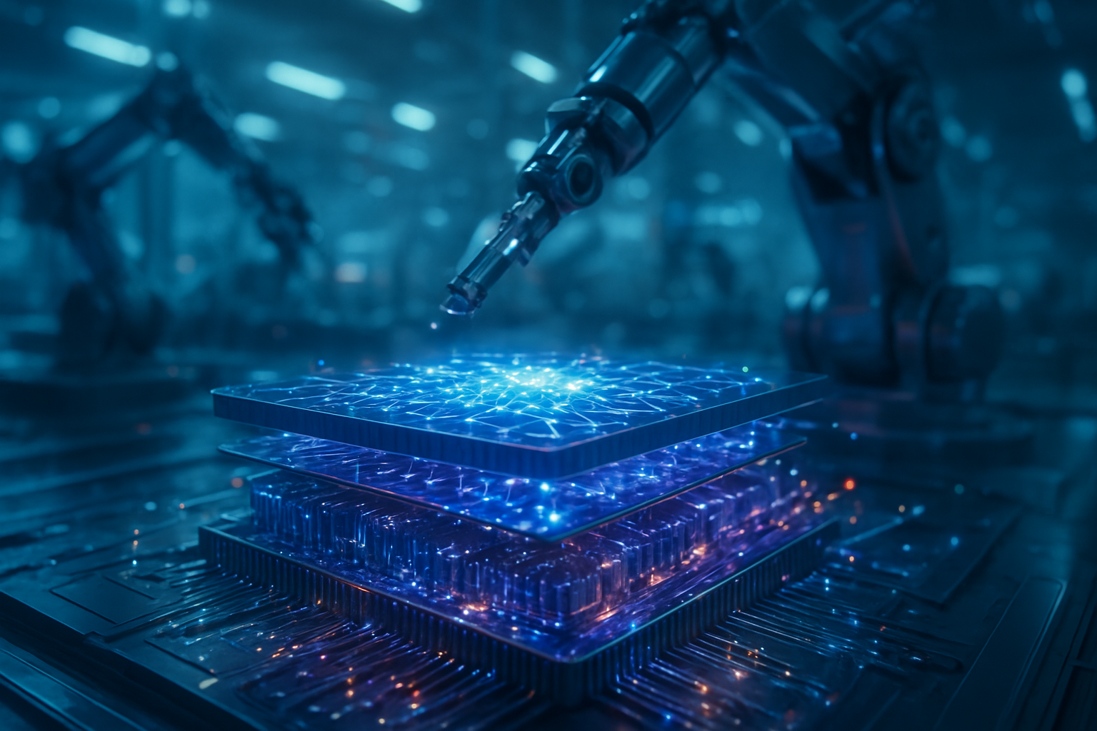
As of January 2, 2026, the artificial intelligence landscape has officially shifted from a focus on conversational "chatbots" to the era of the "agentic" workforce. Leading this charge is Anthropic, whose latest Claude 4.5 model has demonstrated a level of digital autonomy that was considered theoretical only 18 months ago. By maturing its "Computer Use" capability, Anthropic has transformed the model into a reliable "digital intern" capable of navigating complex operating systems with the precision and logic previously reserved for human junior associates.
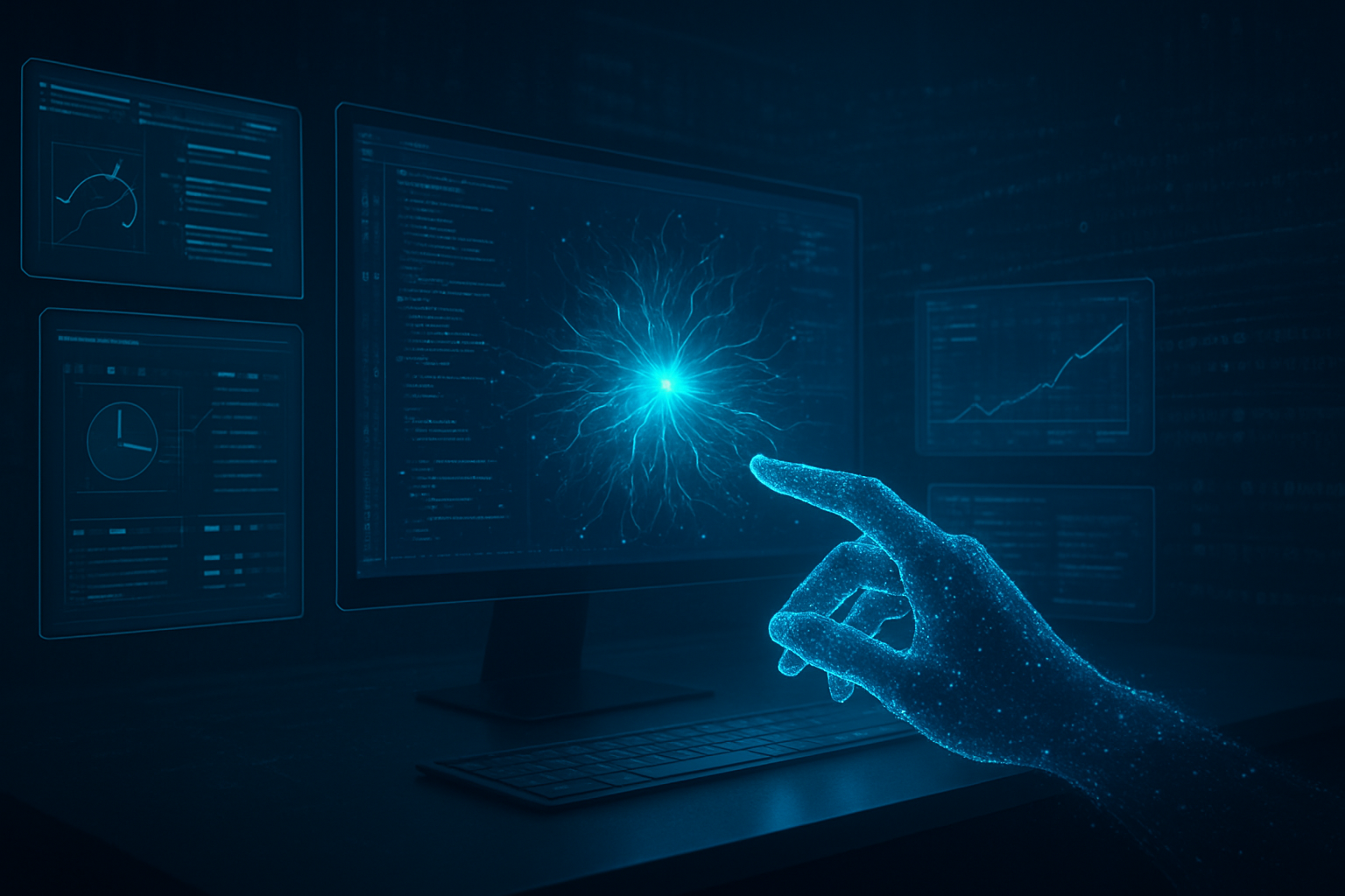
The significance of this development cannot be overstated for enterprise efficiency. Unlike previous iterations of automation that relied on rigid APIs or brittle scripts, Claude 4.5 interacts with computers the same way humans do: by looking at a screen, moving a cursor, clicking buttons, and typing text. This leap in capability allows the model to bridge the gap between disparate software tools that don't natively talk to each other, effectively acting as the connective tissue for modern business workflows.
The Technical Leap: Crossing the 60% OSWorld Threshold
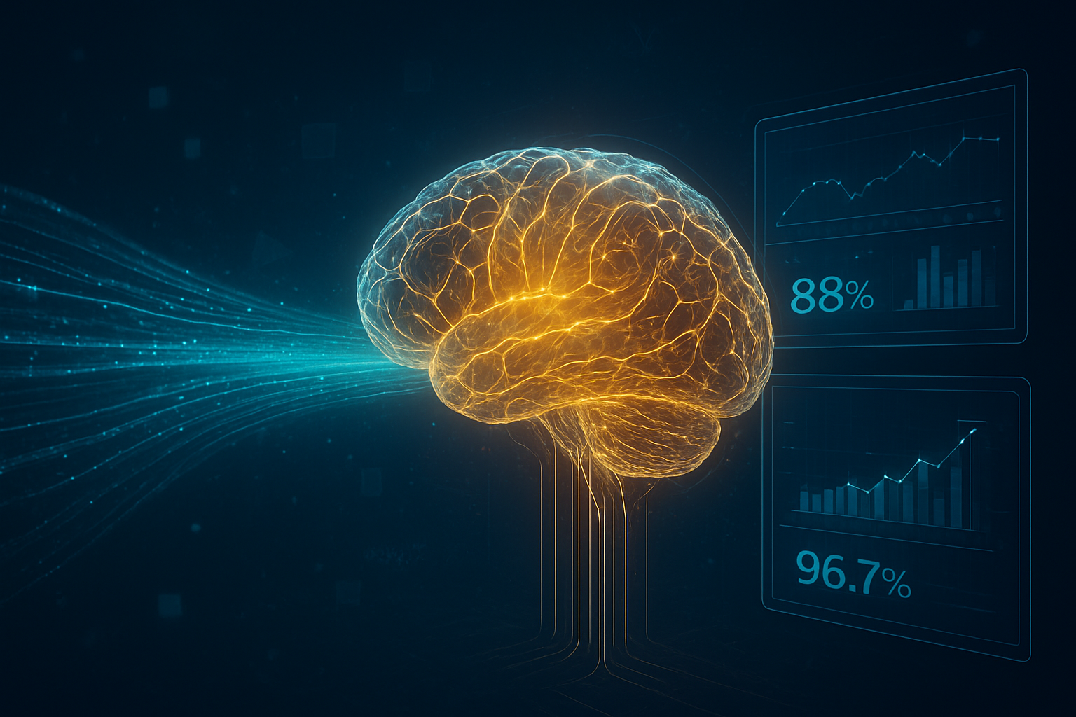
At the heart of Claude 4.5’s maturation is its staggering performance on the OSWorld benchmark. While Claude 3.5 Sonnet broke ground in late 2024 with a modest success rate of roughly 14.9%, Claude 4.5 has achieved a 61.4% success rate. This metric is critical because it tests an AI's ability to complete multi-step, open-ended tasks across real-world applications like web browsers, spreadsheets, and professional design tools. Reaching the 60% mark is widely viewed by researchers as the "utility threshold"—the point at which an AI becomes reliable enough to perform tasks without constant human hand-holding.
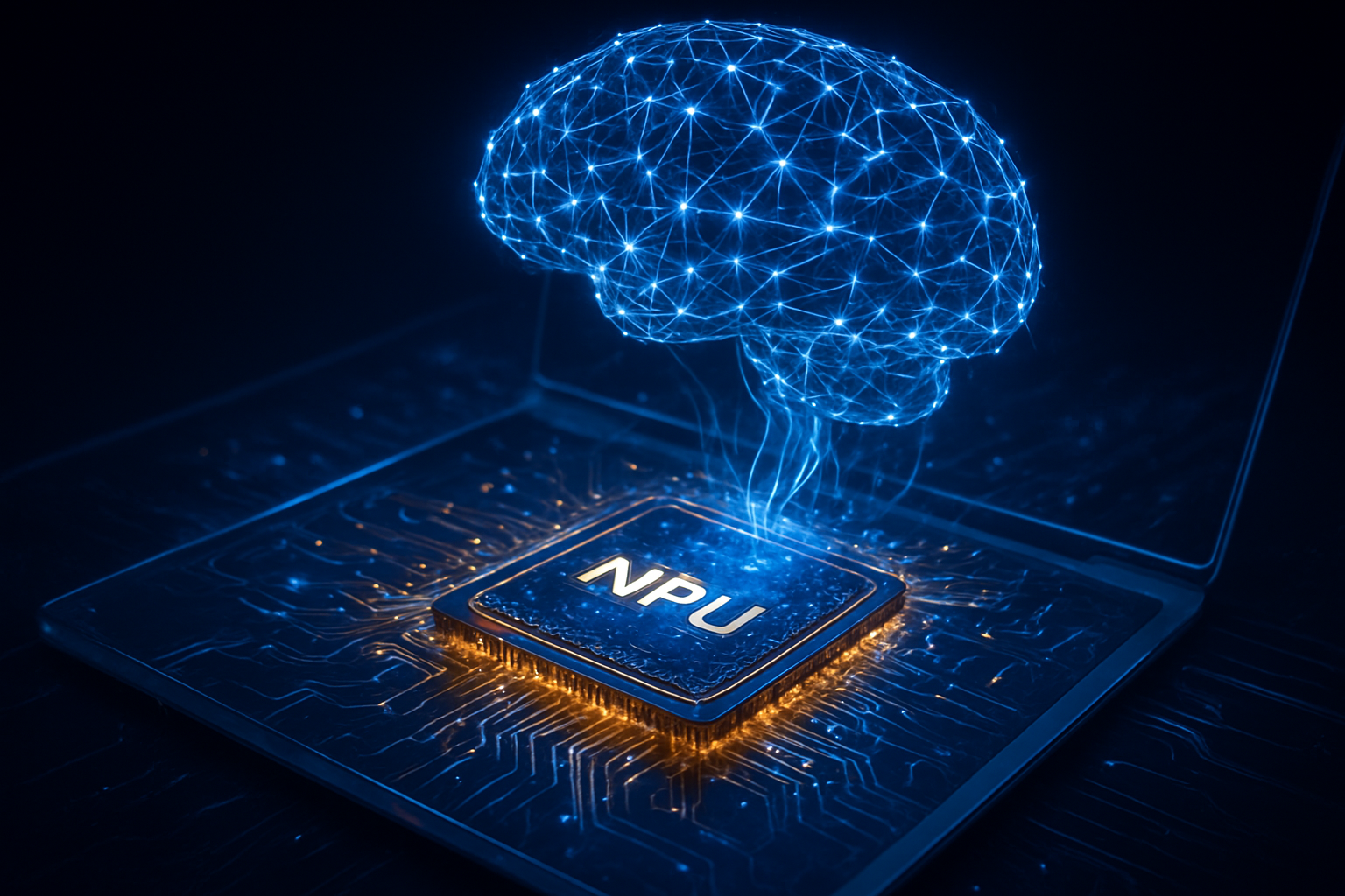
This technical achievement is powered by the new Claude Agent SDK, a developer toolkit that provides the infrastructure for these "digital interns." The SDK introduces "Infinite Context Summary," which allows the model to maintain a coherent memory of its actions over sessions lasting dozens of hours, and "Computer Use Zoom," a feature that allows the model to "focus" on high-density UI elements like tiny cells in a complex financial model. Furthermore, the model now employs "semantic spatial reasoning," allowing it to understand that a "Submit" button is still a "Submit" button even if it is partially obscured or changes color in a software update.
Initial reactions from the AI research community have been overwhelmingly positive, with many noting that Anthropic has solved the "hallucination drift" that plagued earlier agents. By implementing a system of "Checkpoints," the Claude Agent SDK allows the model to save its state and roll back to a previous point if it encounters an unexpected UI error or pop-up. This self-correcting mechanism is what has allowed Claude 4.5 to move from a 15% success rate to over 60% in just over a year of development.
The Enterprise Ecosystem: GitLab, Canva, and the New SaaS Standard
The maturation of Computer Use has fundamentally altered the strategic positioning of major software platforms. Companies like GitLab (NASDAQ: GTLB) have moved beyond simple code suggestions to integrate Claude 4.5 directly into their CI/CD pipelines. The "GitLab Duo Agent Platform" now utilizes Claude to autonomously identify bugs, write the necessary code, and open Merge Requests without human intervention. This shift has turned GitLab from a repository host into an active participant in the development lifecycle.
Similarly, Canva and Replit have leveraged Claude 4.5 to redefine user experience. Canva has integrated the model as a "Creative Operating System," where users can simply describe a multi-channel marketing campaign, and Claude will autonomously navigate the Canva GUI to create brand kits, social posts, and video templates. Replit (Private) has seen similar success with its Replit Agent 3, which can now run for up to 200 minutes autonomously to build and deploy full-stack applications, fetching data from external APIs and navigating third-party dashboards to set up hosting environments.
This development places immense pressure on tech giants like Microsoft (NASDAQ: MSFT) and Google (NASDAQ: GOOGL). While both have integrated "Copilots" into their respective ecosystems, Anthropic’s model-agnostic approach to "Computer Use" allows Claude to operate across any software environment, not just those owned by a single provider. This flexibility has made Claude 4.5 the preferred choice for enterprises that rely on a diverse "best-of-breed" software stack rather than a single-vendor ecosystem.
A Watershed Moment in the AI Landscape
The rise of the digital intern fits into a broader trend toward "Action-Oriented AI." For the past three years, the industry has focused on the "Brain" (the Large Language Model), but Anthropic has successfully provided that brain with "Hands." This transition mirrors previous milestones like the introduction of the graphical user interface (GUI) itself; just as the mouse made computers accessible to the masses, "Computer Use" makes the entire digital world accessible to AI agents.
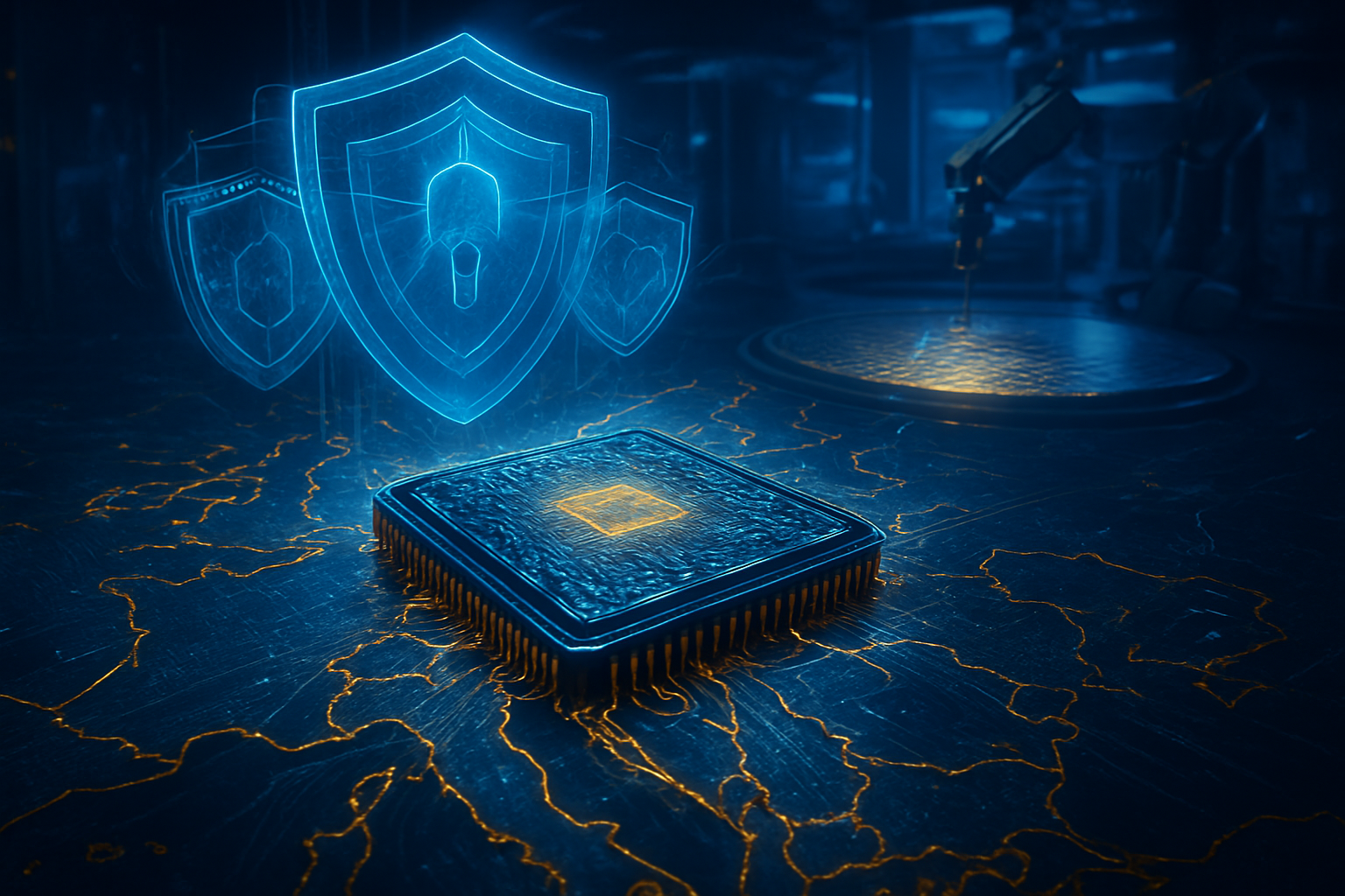
However, this level of autonomy brings significant security and privacy concerns. Giving an AI model the ability to move a cursor and type text is effectively giving it the keys to a digital kingdom. Anthropic has addressed this through "Sandboxed Environments" within the Claude Agent SDK, ensuring that agents run in isolated "clean rooms" where they cannot access sensitive local data unless explicitly permitted. Despite these safeguards, the industry remains in a heated debate over the "human-in-the-loop" requirement, with some regulators calling for mandatory pauses or "kill switches" for autonomous agents.
Comparatively, this breakthrough is being viewed as the "GPT-4 moment" for agents. While GPT-4 proved that AI could reason at a human level, Claude 4.5 is proving that AI can act at a human level. The ability to navigate a messy, real-world desktop environment is a much harder problem than predicting the next word in a sentence, and the 61.4% OSWorld score is the first empirical proof that this problem is being solved.
The Path to Claude 5 and Beyond
Looking ahead, the next frontier for Anthropic will likely be multi-device coordination and even higher levels of OS integration. Near-term developments are expected to focus on "Agent Swarms," where multiple Claude 4.5 instances work together on a single project—for example, one agent handling the data analysis in Excel while another drafts the presentation in PowerPoint and a third manages the email communication with stakeholders.
The long-term vision involves "Zero-Latency Interaction," where the model no longer needs to take screenshots and "think" before each move, but instead flows through a digital environment as fluidly as a human. Experts predict that by the time Claude 5 is released, the OSWorld success rate could top 80%, effectively matching human performance. The primary challenge remains the "edge case" problem—handling the infinite variety of ways a website or application can break or change—but with the current trajectory, these hurdles appear increasingly surmountable.
Conclusion: A New Chapter for Productivity
Anthropic’s Claude 4.5 represents a definitive maturation of the AI agent. By achieving a 61.4% success rate on the OSWorld benchmark and providing the robust Claude Agent SDK, the company has moved the conversation from "what AI can say" to "what AI can do." For enterprises, this means the arrival of the "digital intern"—a tool that can handle the repetitive, cross-platform drudgery that has long been a bottleneck for productivity.
In the history of artificial intelligence, the maturation of "Computer Use" will likely be remembered as the moment AI became truly useful in a practical, everyday sense. As GitLab, Canva, and Replit lead the first wave of adoption, the coming weeks and months will likely see an explosion of similar integrations across every sector of the economy. The "Agentic Era" is no longer a future prediction; it is a present reality.
This content is intended for informational purposes only and represents analysis of current AI developments.
TokenRing AI delivers enterprise-grade solutions for multi-agent AI workflow orchestration, AI-powered development tools, and seamless remote collaboration platforms.
For more information, visit https://www.tokenring.ai/.