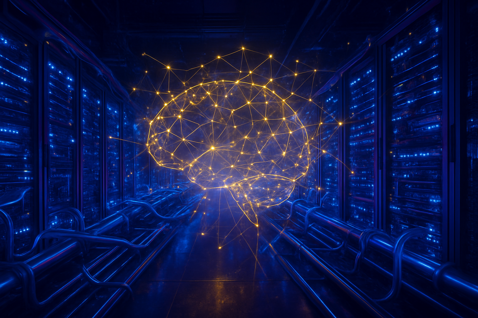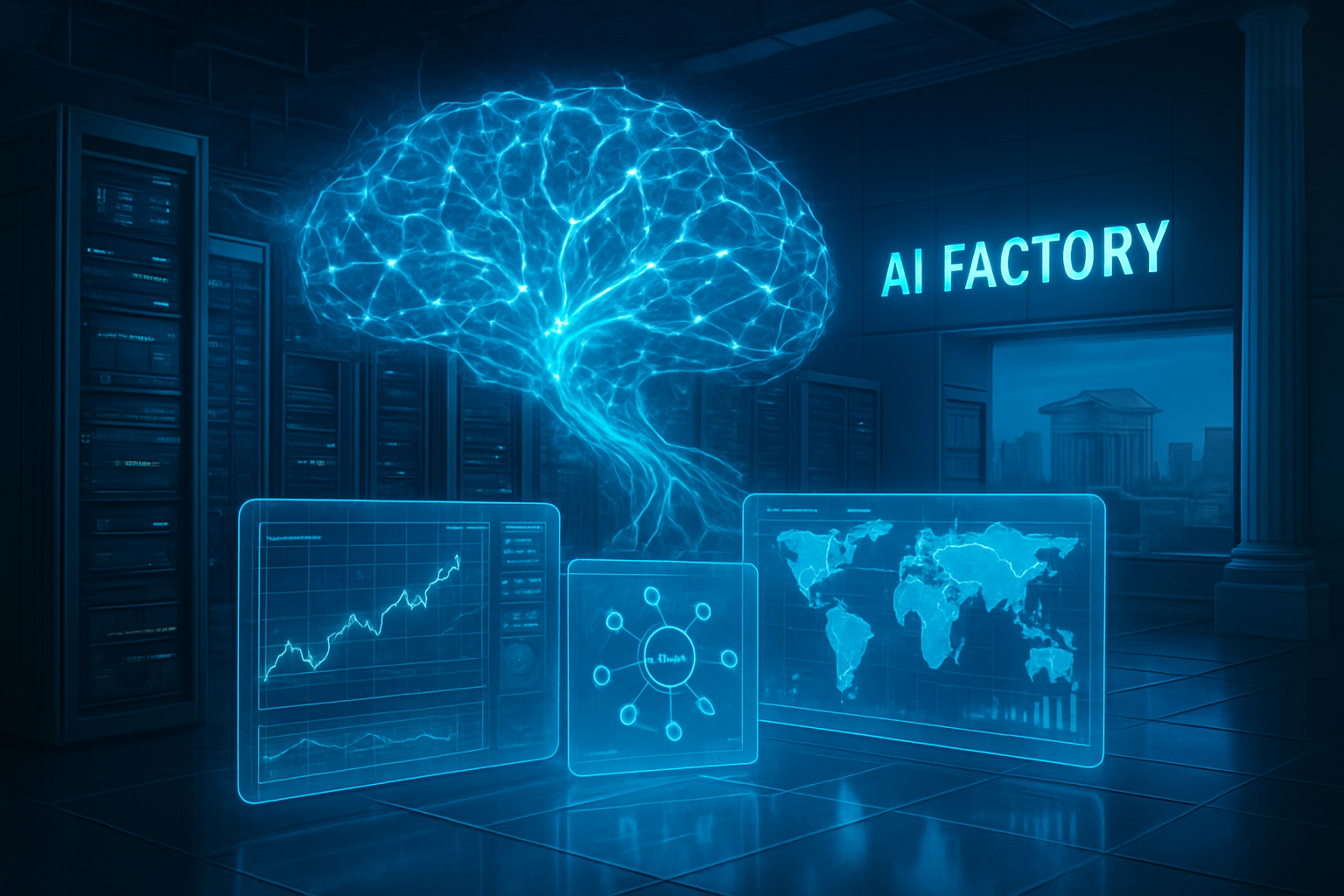
As of early 2026, the artificial intelligence landscape has been fundamentally re-architected. What began as a hardware announcement in mid-2024 has evolved into the central nervous system of the global digital economy: the NVIDIA Blackwell B200 architecture. Today, the deployment of Blackwell is no longer a matter of "if" but "how much," as nations and tech giants scramble to secure their place in the "AI Factory" era. The sheer scale of this deployment has shifted the industry's focus from mere chatbots to massive, agentic systems capable of complex reasoning and multi-step problem solving.
The immediate significance of the Blackwell rollout cannot be overstated. By breaking the physical limits of traditional silicon manufacturing, NVIDIA (NASDAQ:NVDA) has effectively reset the "Scaling Laws" of AI. In early 2026, the B200 is the primary engine behind the world’s most advanced models, including the successors to GPT-4 and Llama 3. Its ability to process trillion-parameter models with unprecedented efficiency has turned what were once experimental research projects into viable, real-time consumer and enterprise applications, fundamentally altering the competitive dynamics of the entire technology sector.
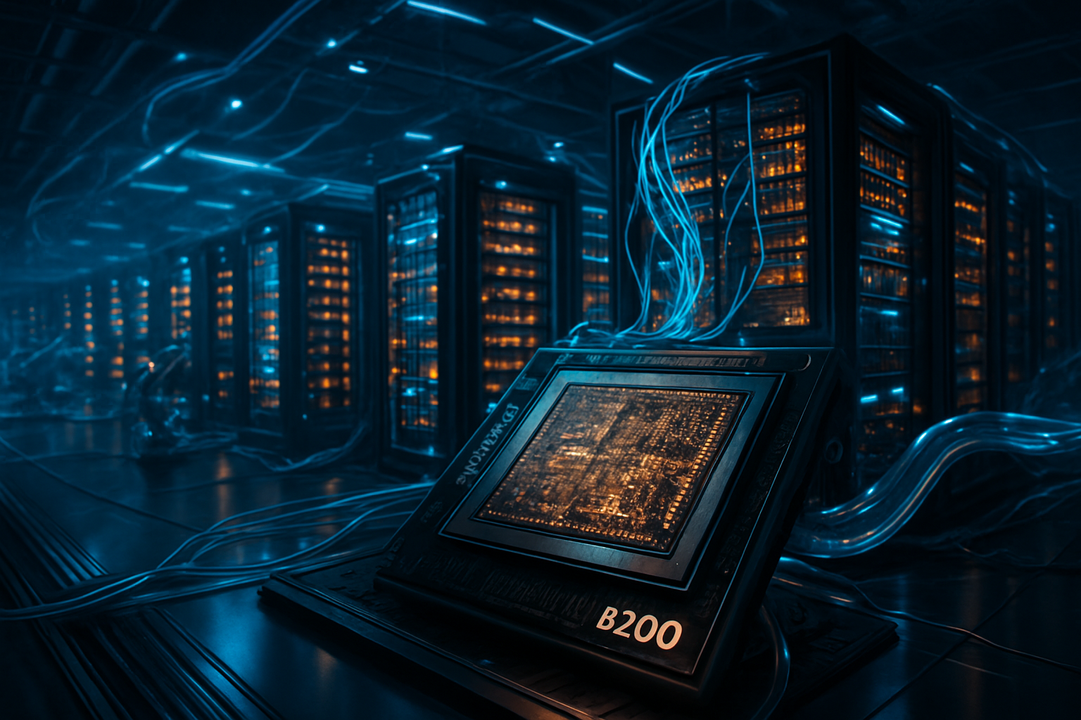
The Silicon Masterpiece: 208 Billion Transistors and the 30x Leap
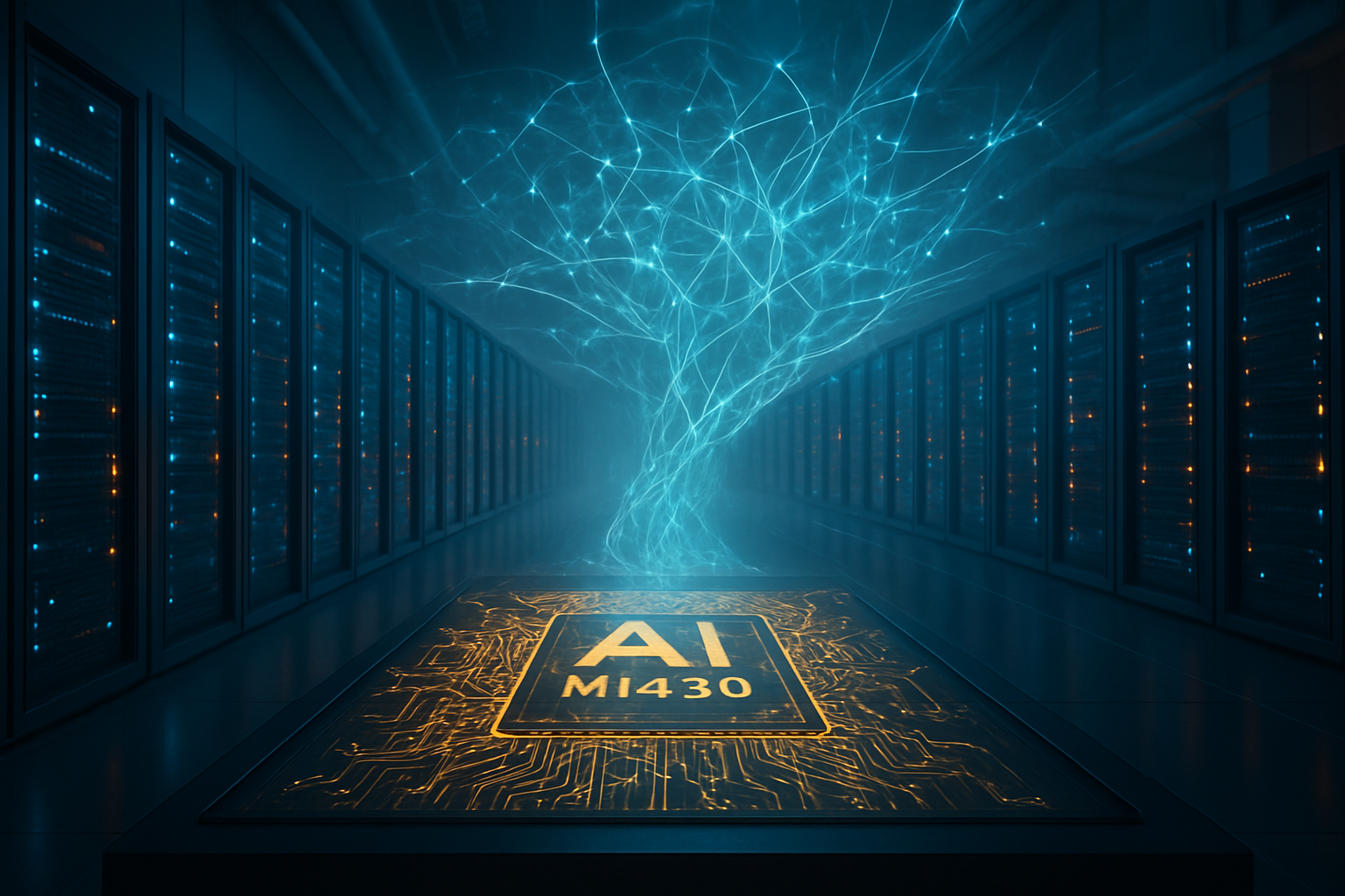
At the heart of the Blackwell revolution is a technical achievement that many skeptics thought impossible just years ago. The B200 GPU utilizes a dual-die chiplet design, fusing two massive silicon dies into a single unified processor via a 10 TB/s chip-to-chip interconnect. This architecture houses a staggering 208 billion transistors—nearly triple the count of the previous-generation H100 "Hopper" architecture. By bypassing the "reticle limit" of a single silicon wafer, NVIDIA has created a processor that functions as a single, cohesive unit while delivering compute density that was previously only possible in multi-node clusters.
The most discussed metric in early 2026 remains NVIDIA’s "30x performance increase" for Large Language Model (LLM) inference. While this figure specifically targets 1.8 trillion-parameter Mixture-of-Experts (MoE) models, its real-world impact is profound. The B200 achieves this through the introduction of a second-generation Transformer Engine and native support for FP4 and FP6 precision. By reducing the numerical precision required for inference without sacrificing model accuracy, Blackwell can deliver nearly double the compute throughput of FP8, allowing for the real-time operation of models that previously "choked" on H100 hardware due to memory and interconnect bottlenecks.
Initial reactions from the AI research community have shifted from awe to a pragmatic focus on system-level scaling. Researchers at labs like OpenAI and Anthropic have noted that the GB200 NVL72—a liquid-cooled rack that treats 72 GPUs as a single unit—has effectively "broken the inference wall." This system-level approach, providing 1.4 exaflops of AI performance in a single rack, has allowed for the transition from simple text prediction to "Agentic AI." These models can now engage in extensive "Chain of Thought" reasoning, making them significantly more capable at tasks involving coding, scientific discovery, and complex logistics.
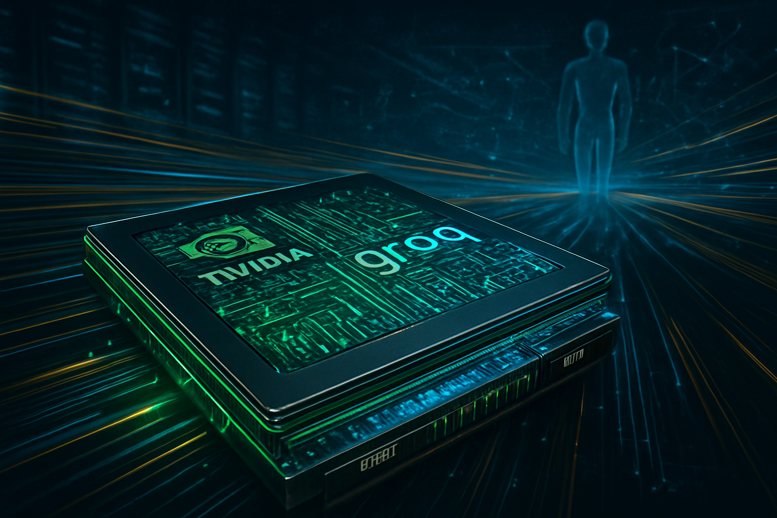
The Compute Divide: Hyperscalers, Startups, and the Rise of AMD
The deployment of Blackwell has created a distinct "compute divide" in the tech industry. For hyperscalers like Microsoft (NASDAQ:MSFT), Alphabet (NASDAQ:GOOGL), and Meta (NASDAQ:META), Blackwell is the cornerstone of their 2026 infrastructure. Microsoft remains the lead customer, utilizing the Azure ND GB200 V6 series to power the next generation of "reasoning" models. Meanwhile, Meta has deployed hundreds of thousands of B200 units to train Llama 4, leveraging the 1.8 TB/s NVLink interconnect to maintain data synchronization across massive clusters.
However, the dominance of Blackwell has also catalyzed a surge in "silicon diversity." As NVIDIA’s chips remain sold out through mid-2026, competitors like AMD (NASDAQ:AMD) have found a significant opening. The AMD Instinct MI355X, built on a 3nm process, has achieved performance parity with Blackwell in several key benchmarks, particularly in memory-intensive tasks. Many AI startups, wary of the "NVIDIA tax" and the high cost of liquid-cooled Blackwell racks, are increasingly turning to AMD’s ROCm 7 software stack. This shift has positioned AMD as the definitive "second source" for high-end AI compute, offering a better "tokens-per-dollar" ratio for specialized applications.
For startups, the Blackwell era is a double-edged sword. While the increased performance makes it cheaper to run advanced models via API, the capital requirements to own and operate Blackwell hardware are prohibitive. This has led to the rise of "neoclouds" like CoreWeave and Lambda, which specialize in providing flexible access to Blackwell clusters. Those who cannot secure Blackwell or high-end AMD hardware are finding themselves forced to innovate in "small model" efficiency or edge-based AI, leading to a vibrant ecosystem of specialized, efficient models that complement the massive frontier models trained on Blackwell.
The Energy Wall and the Sovereign AI Movement
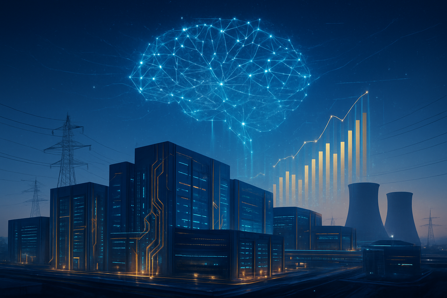
The wider significance of the Blackwell deployment is perhaps most visible in the global energy sector. A single Blackwell B200 GPU consumes approximately 1,200W, and a fully loaded GB200 NVL72 rack exceeds 120kW. This extreme power density has made traditional air cooling obsolete for high-end AI data centers. By early 2026, liquid cooling has become a mandatory standard for more than half of all new data center builds, driving massive growth for infrastructure providers like Equinix (NASDAQ:EQIX) and Digital Realty (NYSE:DLR).
This "energy wall" has forced tech giants to become energy companies. In a trend that has accelerated throughout 2025 and into 2026, companies like Microsoft and Google have signed landmark deals for Small Modular Reactors (SMRs) and nuclear restarts to secure 24/7 carbon-free power for their Blackwell clusters. The physical limit of the power grid has become the new "bottleneck" for AI growth, replacing the chip shortages of 2023 and 2024.
Simultaneously, the "Sovereign AI" movement has emerged as a major geopolitical force. Nations such as the United Arab Emirates, France, and Canada are investing billions in domestic Blackwell-based infrastructure to ensure data independence and national security. The "Stargate UAE" project, featuring over 100,000 Blackwell units, exemplifies this shift from a "petrodollar" to a "technodollar" economy. These nations are no longer content to rent compute from U.S. hyperscalers; they are building their own "AI Factories" to develop national LLMs in their own languages and according to their own cultural values.
Looking Ahead: The Road to Rubin and Beyond
As Blackwell reaches peak deployment in early 2026, the industry is already looking toward NVIDIA’s next milestone. The company has moved to a relentless one-year product rhythm, with the successor to Blackwell—the Rubin architecture (R100)—scheduled for launch in the second half of 2026. Rubin is expected to feature the new Vera CPU and a shift to HBM4 memory, promising another 3x leap in compute density. This rapid pace of innovation keeps competitors in a perpetually reactive posture, as they struggle to match NVIDIA’s integrated stack of silicon, interconnects, and software.
The near-term focus for 2026 will be the refinement of "Physical AI" and robotics. With the compute headroom provided by Blackwell, researchers are beginning to apply the same scaling laws that transformed language to the world of robotics. We are seeing the first generation of humanoid robots powered by "Blackwell-class" edge compute, capable of learning complex tasks through observation rather than explicit programming. The challenge remains the physical hardware—the actuators and batteries—but the "brain" of these systems is no longer the limiting factor.
Experts predict that the next major hurdle will be data scarcity. As Blackwell-powered clusters exhaust the supply of high-quality human-generated text, the industry is pivoting toward synthetic data generation and "self-play" mechanisms, similar to how AlphaGo learned to master the game of Go. The success of these techniques will determine whether the 30x performance gains of Blackwell can be translated into a 30x increase in AI intelligence, or if we are approaching a plateau in the effectiveness of raw scale.
Conclusion: A Milestone in Computing History
The deployment of NVIDIA’s Blackwell architecture marks a definitive chapter in the history of computing. By packing 208 billion transistors into a dual-die system and delivering a 30x leap in inference performance, NVIDIA has not just released a new chip; it has inaugurated the era of the "AI Factory." The transition to liquid cooling, the resurgence of nuclear power, and the rise of sovereign AI are all direct consequences of the Blackwell rollout, reflecting the profound impact this technology has on global infrastructure and geopolitics.
In the coming months, the focus will shift from the deployment of these chips to the output they produce. As the first "Blackwell-native" models begin to emerge, we will see the true potential of agentic AI and its ability to solve problems that were previously beyond the reach of silicon. While the "energy wall" and competitive pressures from AMD and custom silicon remain significant challenges, the Blackwell B200 has solidified its place as the foundational technology of the mid-2020s.
The Blackwell era is just beginning, but its legacy is already clear: it has turned the promise of artificial intelligence into a physical, industrial reality. As we move further into 2026, the world will be watching to see how this unprecedented concentration of compute power reshapes everything from scientific research to the nature of work itself.
This content is intended for informational purposes only and represents analysis of current AI developments.
TokenRing AI delivers enterprise-grade solutions for multi-agent AI workflow orchestration, AI-powered development tools, and seamless remote collaboration platforms.
For more information, visit https://www.tokenring.ai/.