On October 21, 2025, OpenAI fundamentally shifted the landscape of digital navigation with the release of Atlas, an AI-native browser designed to replace the traditional search-and-click model with a paradigm of delegation and autonomous execution. By integrating its most advanced reasoning models directly into the browsing engine, OpenAI is positioning Atlas not just as a tool for viewing the web, but as an agentic workspace capable of performing complex tasks on behalf of the user. The launch marks the most aggressive challenge to the dominance of Google Chrome, owned by Alphabet Inc. (NASDAQ: GOOGL), in over a decade.
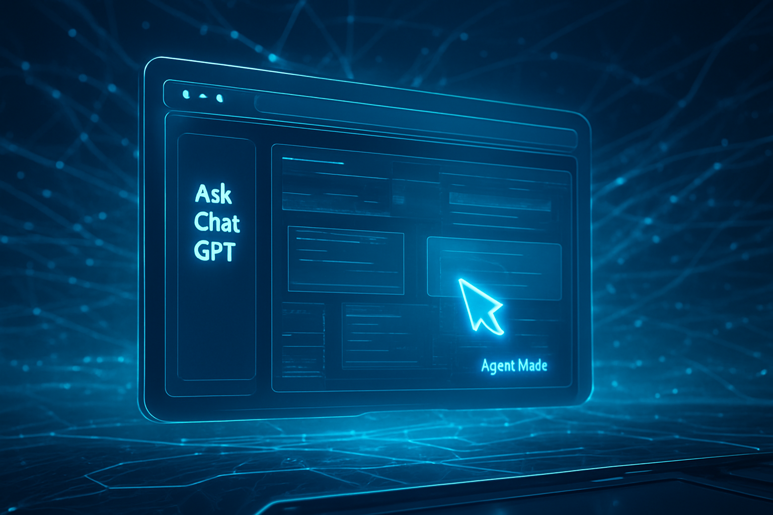
The immediate significance of Atlas lies in its departure from the "tab-heavy" workflow that has defined the internet since the late 1990s. Instead of acting as a passive window to websites, Atlas serves as an active participant. With the introduction of a dedicated "Ask ChatGPT" sidebar and a revolutionary "Agent Mode," the browser can now navigate websites, fill out forms, and synthesize information across multiple domains without the user ever having to leave a single interface. This "agentic" approach suggests a future where the browser is less of a viewer and more of a digital personal assistant.
The OWL Architecture: Engineering a Proactive Web Experience
Technically, Atlas is built on a sophisticated foundation that OpenAI calls the OWL (OpenAI’s Web Layer) architecture. While the browser utilizes the open-source Chromium engine to ensure compatibility with modern web standards and existing extensions, the user interface is a custom-built environment developed using SwiftUI and AppKit. This dual-layer approach allows Atlas to maintain the speed and stability of a traditional browser while running a "heavyweight" local AI sub-runtime in parallel. This sub-runtime includes on-device models like OptGuideOnDeviceModel, which handle real-time page structure analysis and intent recognition without sending every click to the cloud.
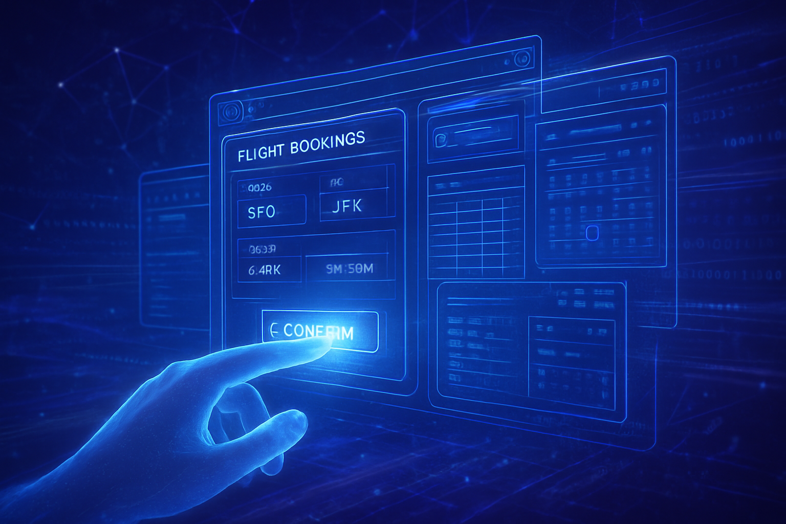
The standout feature of Atlas is its Integrated Agent Mode. When toggled, the browser UI shifts to a distinct blue highlight, and a "second cursor" appears on the screen, representing the AI’s autonomous actions. In this mode, ChatGPT can execute multi-step workflows—such as researching a product, comparing prices across five different retailers, and adding the best option to a shopping cart—while the user watches in real-time. This differs from previous AI "copilots" or plugins, which were often limited to text summarization or basic data scraping. Atlas has the "hand-eye coordination" to interact with dynamic web elements, including JavaScript-heavy buttons and complex drop-down menus.
Initial reactions from the AI research community have been a mix of technical awe and caution. Experts have noted that OpenAI’s ability to map the Document Object Model (DOM) of a webpage directly into a transformer-based reasoning engine represents a significant breakthrough in computer vision and natural language processing. However, the developer community has also pointed out the immense hardware requirements; Atlas is currently exclusive to high-end macOS devices, with Windows and mobile versions still in development.
Strategic Jujitsu: Challenging Alphabet’s Search Hegemony
The release of Atlas is a direct strike at the heart of the business model for Alphabet Inc. (NASDAQ: GOOGL). For decades, Google has relied on the "search-and-click" funnel to drive its multi-billion-dollar advertising engine. By encouraging users to delegate their browsing to an AI agent, OpenAI effectively bypasses the search results page—and the ads that live there. Market analysts observed a 3% to 5% dip in Alphabet’s share price immediately following the Atlas announcement, reflecting investor anxiety over this "disintermediation" of the web.
Beyond Google, the move places pressure on Microsoft (NASDAQ: MSFT), OpenAI’s primary partner. While Microsoft has integrated GPT technology into its Edge browser, Atlas represents a more radical, "clean-sheet" design that may eventually compete for the same user base. Apple (NASDAQ: AAPL) also finds itself in a complex position; while Atlas is currently a macOS-exclusive power tool, its success could force Apple to accelerate the integration of "Apple Intelligence" into Safari to prevent a mass exodus of its most productive users.
For startups and smaller AI labs, Atlas sets a daunting new bar. Companies like Perplexity AI, which recently launched its own 'Comet' browser, now face a competitor with deeper model integration and a massive existing user base of ChatGPT Plus subscribers. OpenAI is leveraging a freemium model to capture the market, keeping basic browsing free while locking the high-utility Agent Mode behind its $20-per-month subscription tiers, creating a high-margin recurring revenue stream that traditional browsers lack.
The End of the Open Web? Privacy and Security in the Agentic Era
The wider significance of Atlas extends beyond market shares and into the very philosophy of the internet. By using "Browser Memories" to track user habits and research patterns, OpenAI is creating a hyper-personalized web experience. However, this has sparked intense debate about the "anti-web" nature of AI browsers. Critics argue that by summarizing and interacting with sites on behalf of users, Atlas could starve content creators of traffic and ad revenue, potentially leading to a "hollowed-out" internet where only the most AI-friendly sites survive.
Security concerns have also taken center stage. Shortly after launch, researchers identified a vulnerability known as "Tainted Memories," where malicious websites could inject hidden instructions into the AI’s persistent memory. These instructions could theoretically prompt the AI to leak sensitive data or perform unauthorized actions in future sessions. This highlights a fundamental challenge: as browsers become more autonomous, they also become more susceptible to complex social engineering and prompt injection attacks that traditional firewalls and antivirus software are not yet equipped to handle.
Comparisons are already being drawn to the "Mosaic moment" of 1993. Just as Mosaic made the web accessible to the masses through a graphical interface, Atlas aims to make the web "executable" through a conversational interface. It represents a shift from the Information Age to the Agentic Age, where the value of a tool is measured not by how much information it provides, but by how much work it completes.
The Road Ahead: Multi-Agent Orchestration and Mobile Horizons
Looking forward, the evolution of Atlas is expected to focus on "multi-agent orchestration." In the near term, OpenAI plans to allow Atlas to communicate with other AI agents—such as those used by travel agencies or corporate internal tools—to negotiate and complete tasks with even less human oversight. We are likely to see the browser move from a single-tab experience to a "workspace" model, where the AI manages dozens of background tasks simultaneously, providing the user with a curated summary of completed actions at the end of the day.
The long-term challenge for OpenAI will be the transition to mobile. While Atlas is a powerhouse on the desktop, the constraints of mobile operating systems and battery life pose significant hurdles for running heavy local AI runtimes. Experts predict that OpenAI will eventually release a "lite" version of Atlas for iOS and Android that relies more heavily on cloud-based inference, though this may run into friction with the strict app store policies maintained by Apple and Google.
A New Map for the Digital World
OpenAI’s Atlas is more than just another browser; it is an attempt to redefine the interface between humanity and the sum of digital knowledge. By moving the AI from a chat box into the very engine we use to navigate the world, OpenAI has created a tool that prioritizes outcomes over exploration. The key takeaways from this launch are clear: the era of "searching" is being eclipsed by the era of "doing," and the browser has become the primary battlefield for AI supremacy.
As we move into 2026, the industry will be watching closely to see how Google responds with its own AI-integrated Chrome updates and whether OpenAI can resolve the significant security and privacy hurdles inherent in autonomous browsing. For now, Atlas stands as a monumental development in AI history—a bold bet that the future of the internet will not be browsed, but commanded.
This content is intended for informational purposes only and represents analysis of current AI developments.
TokenRing AI delivers enterprise-grade solutions for multi-agent AI workflow orchestration, AI-powered development tools, and seamless remote collaboration platforms.
For more information, visit https://www.tokenring.ai/.