As of late December 2025, Apple Inc. (NASDAQ: AAPL) has fundamentally altered the trajectory of the consumer technology industry. What began as a cautious entry into the generative AI space at WWDC 2024 has matured into a comprehensive ecosystem known as "Apple Intelligence." By deeply embedding artificial intelligence into the core of iOS 19, iPadOS 19, and macOS 16, Apple has successfully moved AI from a novelty chat interface into a seamless, proactive layer of the operating system that millions of users now interact with daily.
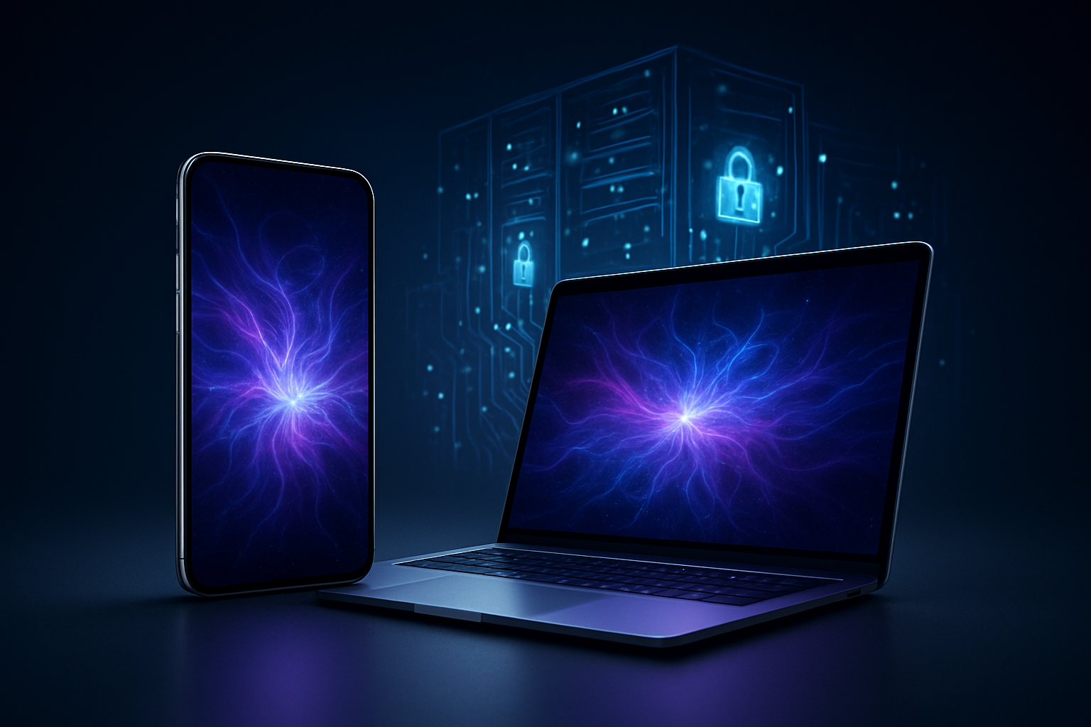
The significance of this development cannot be overstated. By prioritizing on-device processing and pioneering the "Private Cloud Compute" (PCC) architecture, Apple has effectively addressed the primary consumer concern surrounding AI: privacy. This strategic positioning, combined with a high-profile partnership with OpenAI and the recent introduction of the "Apple Intelligence Pro" subscription tier, has propelled Apple to a historic $4 trillion market capitalization, cementing its lead in the "Edge AI" race.
The Technical Architecture: On-Device Prowess and the M5 Revolution
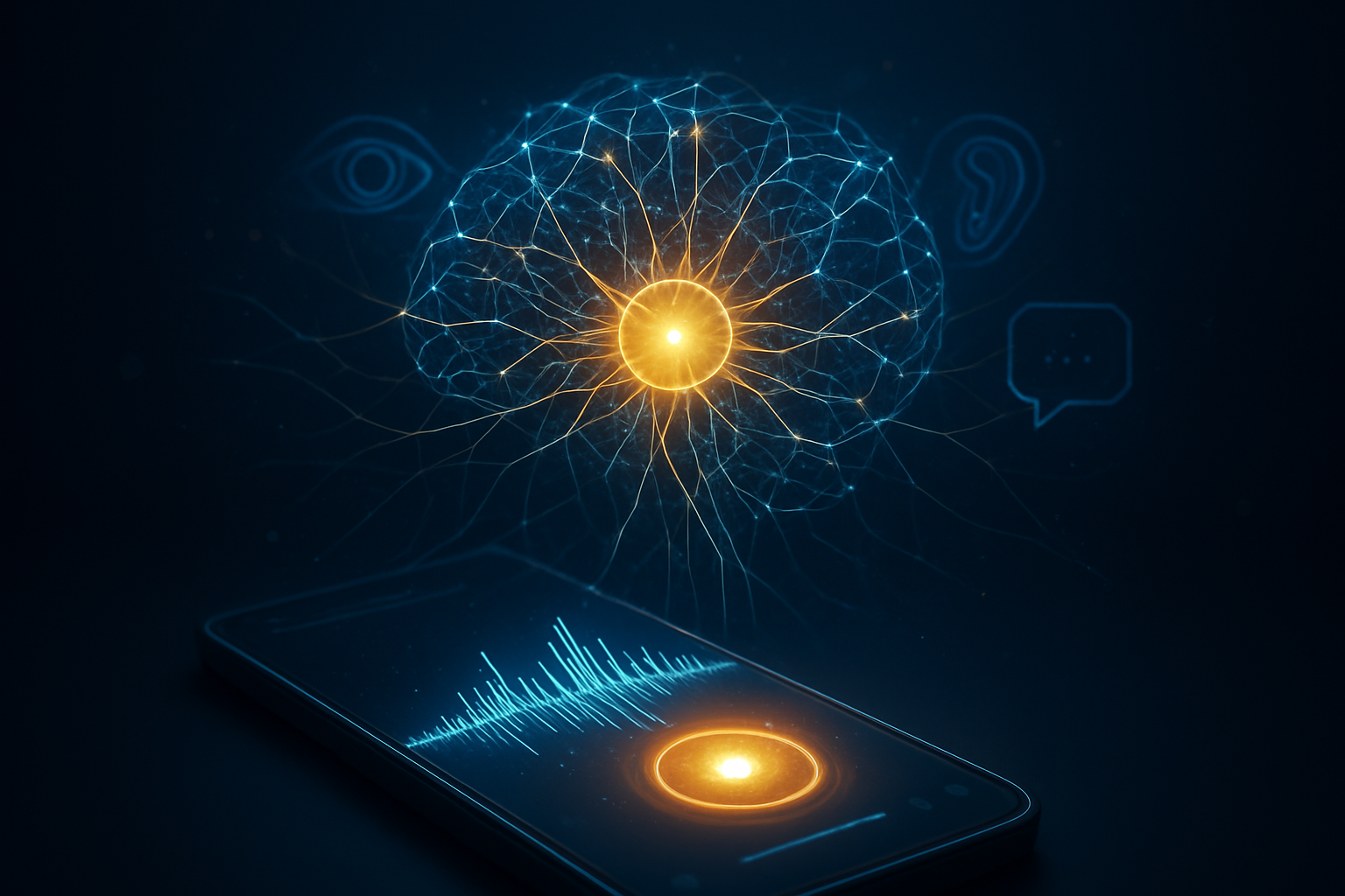
The current state of Apple Intelligence in late 2025 is defined by the sheer power of Apple’s silicon. The newly released M5 and A19 Pro chips feature dedicated "Neural Accelerators" that have quadrupled the AI compute performance compared to the previous generation. This hardware leap allows for the majority of Apple Intelligence tasks—such as text summarization, Genmoji creation, and real-time "Visual Intelligence" on the iPhone 17—to occur entirely on-device. This "on-device first" approach differs from the cloud-heavy strategies of competitors by ensuring that personal data never leaves the user's pocket, providing a zero-latency experience that feels instantaneous.
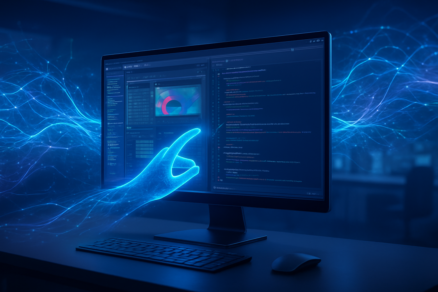
For tasks requiring more significant computational power, Apple utilizes its Private Cloud Compute (PCC) infrastructure. Unlike traditional cloud AI, PCC operates on a "stateless" model where data is wiped the moment a request is fulfilled, a claim that has been rigorously verified by independent security researchers throughout 2025. This year also saw the opening of the Private Cloud API, allowing third-party developers to run complex models on Apple’s silicon servers for free, effectively democratizing high-end AI development for the indie app community.
Siri has undergone its most radical transformation since its inception in 2011. Under the leadership of Mike Rockwell, the assistant now features "Onscreen Awareness" and "App Intent," enabling it to understand context across different applications. Users can now give complex, multi-step commands like, "Find the contract Sarah sent me on Slack, highlight the changes, and draft a summary for my meeting at 3:00 PM." While the "Full LLM Siri"—a version capable of human-level reasoning—is slated for a spring 2026 release in iOS 19.4, the current iteration has already silenced critics who once viewed Siri as a relic of the past.
Initial reactions from the AI research community have been largely positive, particularly regarding Apple's commitment to verifiable privacy. Dr. Elena Rossi, a leading AI ethicist, noted that "Apple has created a blueprint for how generative AI can coexist with civil liberties, forcing the rest of the industry to rethink their data-harvesting models."
The Market Ripple Effect: "Sherlocking" and the Multi-Model Strategy
The widespread adoption of Apple Intelligence has sent shockwaves through the tech sector, particularly for AI startups. Companies like Grammarly and various AI-based photo editing apps have faced a "Sherlocking" event—where their core features are integrated directly into the OS. Apple’s system-wide "Writing Tools" have commoditized basic AI text editing, leading to a significant shift in the startup landscape. Successful developers in 2025 have pivoted away from "wrapper" apps, instead focusing on "Apple Intelligence Integrations" that leverage Apple's local Foundation Models Framework.
Strategically, Apple has moved from an "OpenAI-first" approach to a "Multi-AI Platform" model. While the partnership with OpenAI remains a cornerstone—integrating the latest ChatGPT-5 capabilities for world-knowledge queries—Apple has also finalized deals with Alphabet Inc. (NASDAQ: GOOGL) to integrate Gemini as a search-focused alternative. Furthermore, the adoption of Anthropic’s Model Context Protocol (MCP) allows power users to "plugin" their preferred AI models, such as Claude, to interact directly with their device’s data. This has turned Apple Intelligence into an "AI Orchestrator," positioning Apple as the gatekeeper of the AI user experience.
The hardware market has also felt the impact. While NVIDIA (NASDAQ: NVDA) continues to dominate the high-end researcher market with its Blackwell architecture, Apple's efficiency-first approach has pressured other chipmakers. Qualcomm (NASDAQ: QCOM) has emerged as the primary rival in the "AI PC" space, with its Snapdragon X2 Elite chips challenging the MacBook's dominance in battery life and NPU performance. Microsoft (NASDAQ: MSFT) has responded by doubling down on "Copilot+ PC" certifications, creating a fierce competitive environment where AI performance-per-watt is the new primary metric for consumers.
The Wider Significance: Privacy as a Luxury and the Death of the App
Apple Intelligence represents a shift in the broader AI landscape from "AI as a destination" (like a website or a specific app) to "AI as an ambient utility." This transition marks the beginning of the end for the traditional "app-siloed" experience. In the Apple Intelligence era, the operating system understands the user's intent across all apps, effectively acting as a digital concierge. This has led to concerns about "platform lock-in," as the more a user interacts with Apple Intelligence, the more difficult it becomes to leave the ecosystem due to the deep integration of personal context.
The focus on privacy has also transformed "data security" from a technical specification into a luxury product feature. By marketing Apple Intelligence as the only "truly private" AI, Apple has successfully justified the premium pricing of its hardware and its new subscription models. However, this has also raised questions about the "AI Divide," where advanced privacy and agentic capabilities are increasingly locked behind high-end hardware and "Pro" tier paywalls, potentially leaving budget-conscious consumers with less secure or less capable alternatives.
Comparatively, this milestone is being viewed as the "iPhone moment" for AI. Just as the original iPhone moved the internet from the desktop to the pocket, Apple Intelligence has moved generative AI from the data center to the device. The impact on societal productivity is already being measured, with early reports suggesting a 15-20% increase in efficiency for knowledge workers using integrated AI writing and organizational tools.
Future Horizons: Multimodal Siri and the International Expansion
Looking toward 2026, the roadmap for Apple Intelligence is ambitious. The upcoming iOS 19.4 update is expected to introduce the "Full LLM Siri," which will move away from intent-based programming toward a more flexible, reasoning-based architecture. This will likely enable even more complex autonomous tasks, such as Siri booking travel and managing finances with minimal user intervention.
We also expect to see deeper multimodal integration. While "Visual Intelligence" is currently limited to the camera and Vision Pro, future iterations are expected to allow Apple Intelligence to "see" and understand everything on a user's screen in real-time, providing proactive suggestions before a user even asks. This "proactive agency" is the next frontier for the company.
Challenges remain, however. The international rollout of Apple Intelligence has been slowed by regulatory hurdles, particularly in the European Union and China. Negotiating the balance between Apple’s strict privacy standards and the local data laws of these regions will be a primary focus for Apple’s legal and engineering teams in the coming year. Furthermore, the company must address the "hallucination" problem that still occasionally plagues even the most advanced LLMs, ensuring that Siri remains a reliable source of truth.
Conclusion: A New Paradigm for Human-Computer Interaction
Apple Intelligence has successfully transitioned from a high-stakes gamble to the defining feature of the Apple ecosystem. By the end of 2025, it is clear that Apple’s strategy of "patience and privacy" has paid off. The company did not need to be the first to the AI party; it simply needed to be the one that made AI feel safe, personal, and indispensable.
The key takeaways from this development are the validation of "Edge AI" and the emergence of the "AI OS." Apple has proven that consumers value privacy and seamless integration over raw, unbridled model power. As we move into 2026, the tech world will be watching the adoption rates of "Apple Intelligence Pro" and the impact of the "Full LLM Siri" to see if Apple can maintain its lead.
In the history of artificial intelligence, 2025 will likely be remembered as the year AI became personal. For Apple, it is the year they redefined the relationship between humans and their devices, turning the "Personal Computer" into a "Personal Intelligence."
This content is intended for informational purposes only and represents analysis of current AI developments.
TokenRing AI delivers enterprise-grade solutions for multi-agent AI workflow orchestration, AI-powered development tools, and seamless remote collaboration platforms.
For more information, visit https://www.tokenring.ai/.