Blog

  • OpenAI Declares ‘Code Red’ as GPT-5.2 Launches to Reclaim AI Supremacy

    OpenAI Declares ‘Code Red’ as GPT-5.2 Launches to Reclaim AI Supremacy

    SAN FRANCISCO — In a decisive move to re-establish its dominance in an increasingly fractured artificial intelligence market, OpenAI has officially released GPT-5.2. The new model series, internally codenamed "Garlic," arrived on December 11, 2025, following a frantic internal "code red" effort to counter aggressive breakthroughs from rivals Google and Anthropic. Featuring a massive 256k token context window and a specialized "Thinking" engine for multi-step reasoning, GPT-5.2 marks a strategic shift for OpenAI as it moves away from general-purpose assistants toward highly specialized, agentic professional tools.

    The launch comes at a critical juncture for the AI pioneer. Throughout 2025, OpenAI faced unprecedented pressure as Google’s Gemini 3 and Anthropic’s Claude 4.5 began to eat into its enterprise market share. The "code red" directive, issued by CEO Sam Altman earlier this month, reportedly pivoted the entire company’s focus toward the core ChatGPT experience, pausing secondary projects in advertising and hardware to ensure GPT-5.2 could meet the rising bar for "expert-level" reasoning. The result is a tiered model system that aims to provide the most reliable long-form logic and agentic execution currently available in the industry.

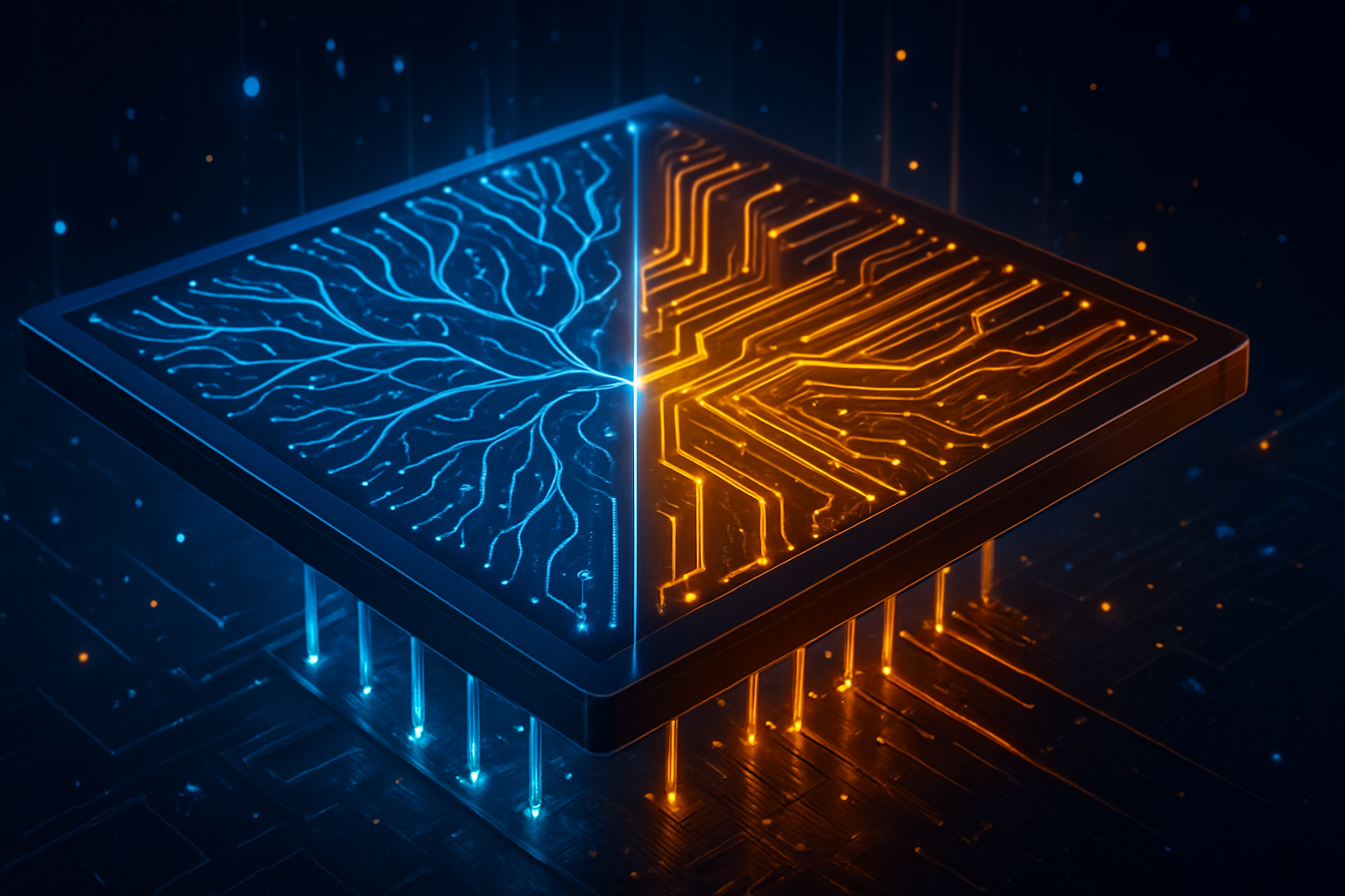
    Technical Prowess: The Dawn of the 'Thinking' Engine

    The technical architecture of GPT-5.2 represents a departure from the "one-size-fits-all" approach of previous generations. OpenAI has introduced three distinct variants: GPT-5.2 Instant, optimized for low-latency tasks; GPT-5.2 Thinking, the flagship reasoning model; and GPT-5.2 Pro, an enterprise-grade powerhouse designed for scientific and financial modeling. The "Thinking" variant is particularly notable for its new "Reasoning Level" parameter, which allows users to dictate how much compute time the model should spend on a problem. At its highest settings, the model can engage in minutes of internal "System 2" deliberation to plan and execute complex, multi-stage workflows without human intervention.

    Key to this new capability is a reliable 256k token context window. While competitors like Meta (NASDAQ: META) have experimented with multi-million token windows, OpenAI has focused on "perfect recall," achieving near 100% accuracy across the full 256k span in internal "needle-in-a-haystack" testing. For massive enterprise datasets, a new /compact endpoint allows for context compaction, effectively extending the usable range to 400k tokens. In terms of benchmarks, GPT-5.2 has set a new high bar, achieving a 100% solve rate on the AIME 2025 math competition and a 70.9% score on the GDPval professional knowledge test, suggesting the model can now perform at or above the level of human experts in complex white-collar tasks.

    Initial reactions from the AI research community have been a mix of awe and caution. Dr. Sarah Chen of the Stanford Institute for Human-Centered AI noted that the "Reasoning Level" parameter is a "game-changer for agentic workflows," as it finally addresses the reliability issues that plagued earlier LLMs. However, some researchers have pointed out a "multimodal gap," observing that while GPT-5.2 excels in text and logic, it still trails Google’s Gemini 3 in native video and audio processing capabilities. Despite this, the consensus is clear: OpenAI has successfully transitioned from a chatbot to a "reasoning engine" capable of navigating the world with unprecedented autonomy.

    A Competitive Counter-Strike: The 'Code Red' Reality

    The launch of GPT-5.2 was born out of necessity rather than a pre-planned roadmap. The internal "code red" was triggered in early December 2025 after Alphabet Inc. (NASDAQ: GOOGL) released Gemini 3, which briefly overtook OpenAI in several key performance metrics and saw Google’s stock surge by over 60% year-to-date. Simultaneously, Anthropic’s Claude 4.5 had secured a 40% market share among corporate developers, who praised its "Skills" protocol for being more reliable in production environments than OpenAI's previous offerings.

    This competitive pressure has forced a realignment among the "Big Tech" players. Microsoft (NASDAQ: MSFT), OpenAI’s largest backer, has moved swiftly to integrate GPT-5.2 into its rebranded "Windows Copilot" ecosystem, hoping to justify the massive capital expenditures that have weighed on its stock performance in 2025. Meanwhile, Nvidia (NASDAQ: NVDA) continues to be the primary beneficiary of this arms race; the demand for its Blackwell architecture remains insatiable as labs rush to train the next generation of "reasoning-first" models. Nvidia's recent acquisition of inference-optimization talent suggests they are also preparing for a future where the cost of "thinking" is as important as the cost of training.

    For startups and smaller AI labs, the arrival of GPT-5.2 is a double-edged sword. While it provides a more powerful foundation to build upon, the "commoditization of intelligence" led by Meta’s open-weight Llama 4 and OpenAI’s tiered pricing is making it harder for mid-tier companies to compete on model performance alone. The strategic advantage has shifted toward those who can orchestrate these models into cohesive, multi-agent workflows—a domain where companies like TokenRing AI are increasingly focused.

    The Broader Landscape: Safety, Speed, and the 'Stargate'

    Beyond the corporate horse race, GPT-5.2’s release has reignited the intense debate over AI safety and the speed of development. Critics, including several former members of OpenAI’s now-dissolved Superalignment team, argue that the "code red" blitz prioritized market dominance over rigorous safety auditing. The concern is that as models gain the ability to "think" for longer periods and execute multi-step plans, the potential for unintended consequences or "agentic drift" increases exponentially. OpenAI has countered these claims by asserting that its new "Reasoning Level" parameter actually makes models safer by allowing for more transparent internal planning.

    In the broader AI landscape, GPT-5.2 fits into a 2025 trend toward "Agentic AI"—systems that don't just talk, but do. This milestone is being compared to the "GPT-3 moment" for autonomous agents. However, this progress is occurring against a backdrop of geopolitical tension. OpenAI recently proposed a "freedom-focused" policy to the U.S. government, arguing for reduced regulatory friction to maintain a lead over international competitors. This move has drawn criticism from AI safety advocates like Geoffrey Hinton, who continues to warn of a 20% chance of existential risk if the current "arms race" remains unchecked by global standards.

    The infrastructure required to support these models is also reaching staggering proportions. OpenAI’s $500 billion "Stargate" joint venture with SoftBank and Oracle (NASDAQ: ORCL) is reportedly ahead of schedule, with a massive compute campus in Abilene, Texas, expected to reach 1 gigawatt of power capacity by mid-2026. This scale of investment suggests that the industry is no longer just building software, but is engaged in the largest industrial project in human history.

    Looking Ahead: GPT-6 and the 'Great Reality Check'

    As the industry digests the capabilities of GPT-5.2, the horizon is already shifting toward 2026. Experts predict that the next major milestone, likely GPT-6, will introduce "Self-Updating Logic" and "Persistent Memory." These features would allow AI models to learn from user interactions in real-time and maintain a continuous "memory" of a user’s history across years, rather than just sessions. This would effectively turn AI assistants into lifelong digital colleagues that evolve alongside their human counterparts.

    However, 2026 is also being dubbed the "Great AI Reality Check." While the intelligence of models like GPT-5.2 is undeniable, many enterprises are finding that their legacy data infrastructures are unable to handle the real-time demands of autonomous agents. Analysts predict that nearly 40% of agentic AI projects may fail by 2027, not because the AI isn't smart enough, but because the "plumbing" of modern business is too fragmented for an agent to navigate effectively. Addressing these integration challenges will be the primary focus for the next wave of AI development tools.

    Conclusion: A New Chapter in the AI Era

    The launch of GPT-5.2 is more than just a model update; it is a declaration of intent. By delivering a system capable of multi-step reasoning and reliable long-context memory, OpenAI has successfully navigated its "code red" crisis and set a new standard for what an "intelligent" system can do. The transition from a chat-based assistant to a reasoning-first agent marks the beginning of a new chapter in AI history—one where the value is found not in the generation of text, but in the execution of complex, expert-level work.

    As we move into 2026, the long-term impact of GPT-5.2 will be measured by how effectively it is integrated into the fabric of the global economy. The "arms race" between OpenAI, Google, and Anthropic shows no signs of slowing down, and the societal questions regarding safety and job displacement remain as urgent as ever. For now, the world is watching to see how these new "thinking" machines will be used—and whether the infrastructure of the human world is ready to keep up with them.


    This content is intended for informational purposes only and represents analysis of current AI developments.

    TokenRing AI delivers enterprise-grade solutions for multi-agent AI workflow orchestration, AI-powered development tools, and seamless remote collaboration platforms.
    For more information, visit https://www.tokenring.ai/.

  • The Backside Revolution: How PowerVia Propels Intel into the Lead of the AI Silicon Race

    The Backside Revolution: How PowerVia Propels Intel into the Lead of the AI Silicon Race

    As the calendar turns to late 2025, the semiconductor industry is witnessing its most profound architectural shift in over a decade. The arrival of Backside Power Delivery (BSPD), spearheaded by Intel Corporation (NASDAQ: INTC) and its proprietary PowerVia technology, has fundamentally altered the physics of chip design. By physically separating power delivery from signal routing, Intel has solved a decade-long "traffic jam" on the silicon wafer, providing a critical performance boost just as the demand for generative AI reaches its zenith.

    This breakthrough is not merely an incremental improvement; it is a total reimagining of how electricity reaches the billions of transistors that power modern AI models. While traditional chips struggle with electrical interference and "voltage drop" as they shrink, PowerVia allows for more efficient power distribution, higher clock speeds, and significantly denser logic. For Intel, this represents a pivotal moment in its "five nodes in four years" strategy, potentially reclaiming the manufacturing crown from long-time rival Taiwan Semiconductor Manufacturing Company (NYSE: TSM).

    Unclogging the Silicon Arteries: The PowerVia Advantage

    For nearly fifty years, chips have been built like a layer cake, with transistors at the bottom and all the wiring—both for data signals and power—layered on top. As transistors shrank to the "Angstrom" scale, these wires became so crowded that they began to interfere with one another. Power lines, which are relatively bulky, would block the path of delicate signal wires, leading to a phenomenon known as "crosstalk" and causing significant voltage drops (IR drop) as electricity struggled to navigate the maze. Intel’s PowerVia solves this by moving the entire power delivery network to the "backside" of the silicon wafer, leaving the "front side" exclusively for data signals.

    Technically, PowerVia achieves this through the use of nano-Through Silicon Vias (nTSVs). These are microscopic vertical tunnels that pass directly through the silicon substrate to connect the backside power layers to the transistors. This approach eliminates the need for power to travel through 10 to 20 layers of metal on the front side. By shortening the path to the transistor, Intel has successfully reduced IR drop by nearly 30%, allowing transistors to switch faster and more reliably. Initial data from Intel’s 18A node, currently in high-volume manufacturing, shows frequency gains of up to 6% at the same power level compared to traditional front-side designs.

    Beyond speed, the removal of power lines from the front side has unlocked a massive amount of "real estate" for logic. Chip designers can now pack transistors much closer together, achieving density improvements of up to 30%. This is a game-changer for AI accelerators, which require massive amounts of logic and memory to process large language models. The industry response has been one of cautious optimism followed by rapid adoption, as experts recognize that BSPD is no longer a luxury, but a necessity for the next generation of high-performance computing.

    A Two-Year Head Start: Intel 18A vs. TSMC A16

    The competitive landscape of late 2025 is defined by a rare "first-mover" advantage for Intel. While Intel’s 18A node is already powering the latest "Panther Lake" consumer chips and "Clearwater Forest" server processors, TSMC is still in the preparation phase for its own BSPD implementation. TSMC has opted to skip a basic backside delivery on its 2nm node, choosing instead to debut an even more advanced version, called Super PowerRail, on its A16 (1.6nm) process. However, A16 is not expected to reach high-volume production until the second half of 2026, giving Intel a roughly 1.5 to 2-year lead in the commercial application of this technology.

    This lead has already begun to shift the strategic positioning of major AI chip designers. Companies that have traditionally relied solely on TSMC, such as NVIDIA Corporation (NASDAQ: NVDA) and Apple Inc. (NASDAQ: AAPL), are now closely monitoring Intel's foundry yields. Intel’s 18A yields are currently reported to be stabilizing between 60% and 70%, a healthy figure for a node of this complexity. The pressure is now on TSMC to prove that its Super PowerRail—which connects power directly to the transistor’s source and drain rather than using Intel's nTSV method—will offer superior efficiency that justifies the wait.

    For the market, this creates a fascinating dynamic. Intel is using its manufacturing lead to lure high-profile foundry customers who are desperate for the power efficiency gains that BSPD provides. Microsoft Corporation (NASDAQ: MSFT) and Amazon.com, Inc. (NASDAQ: AMZN) have already signed on to use Intel’s advanced nodes for their custom AI silicon, such as the Maia 2 and Trainium 2 chips. This disruption to the existing foundry hierarchy could lead to a more diversified supply chain, reducing the industry's heavy reliance on a single geographic region for the world's most advanced chips.

    Powering the AI Infrastructure: Efficiency at Scale

    The wider significance of Backside Power Delivery cannot be overstated in the context of the global AI energy crisis. As data centers consume an ever-increasing share of the world’s electricity, the 15-20% performance-per-watt improvement offered by PowerVia is a critical sustainability tool. For hyperscale cloud providers, a 20% reduction in power consumption translates to hundreds of millions of dollars saved in cooling costs and electricity bills. BSPD is effectively "free performance" that helps mitigate the thermal throttling issues that have plagued high-wattage AI chips like NVIDIA's Blackwell series.

    Furthermore, BSPD enables a new era of "computational density." By clearing the front-side metal layers, engineers can more easily integrate High Bandwidth Memory (HBM) and implement complex chiplet architectures. This allows for larger logic dies on the same interposer, as the power delivery no longer clutters the high-speed interconnects required for chip-to-chip communication. This fits into the broader trend of "system-level" scaling, where the entire package, rather than just the individual transistor, is optimized for AI workloads.

    However, the transition to BSPD is not without its concerns. The manufacturing process is significantly more complex, requiring advanced wafer bonding and thinning techniques that increase the risk of defects. There are also long-term reliability questions regarding the thermal management of the backside power layers, which are now physically closer to the silicon substrate. Despite these challenges, the consensus among AI researchers is that the benefits far outweigh the risks, marking this as a milestone comparable to the introduction of FinFET transistors in the early 2010s.

    The Road to Sub-1nm: What Lies Ahead

    Looking toward 2026 and beyond, the industry is already eyeing the next evolution of power delivery. While Intel’s PowerVia and TSMC’s Super PowerRail are the current gold standard, research is already underway for "direct-to-gate" power delivery, which could further reduce resistance. We expect to see Intel refine its 18A process into "14A" by 2027, potentially introducing even more aggressive backside routing. Meanwhile, TSMC’s A16 will likely be the foundation for the first sub-1nm chips, where BSPD will be an absolute requirement for the transistors to function at all.

    The potential applications for this technology extend beyond the data center. As AI becomes more prevalent in "edge" devices, the power savings of BSPD will enable more sophisticated on-device AI for smartphones and wearable tech without sacrificing battery life. Experts predict that by 2028, every flagship processor in the world—from laptops to autonomous vehicles—will utilize some form of backside power delivery. The challenge for the next three years will be scaling these complex manufacturing processes to meet the insatiable global demand for silicon.

    A New Era of Silicon Sovereignty

    In summary, Backside Power Delivery represents a total architectural pivot that has arrived just in time to sustain the AI revolution. Intel’s PowerVia has provided the company with a much-needed technical edge, proving that its aggressive manufacturing roadmap was more than just marketing rhetoric. By being the first to market with 18A, Intel has forced the rest of the industry to accelerate their timelines, ultimately benefiting the entire ecosystem with more efficient and powerful hardware.

    As we look ahead to the coming months, the focus will shift from technical "proofs of concept" to high-volume execution. Watch for Intel's quarterly earnings reports and foundry updates to see if they can maintain their yield targets, and keep a close eye on TSMC’s A16 risk production milestones in early 2026. This is a marathon, not a sprint, but for the first time in a decade, the lead runner has changed, and the stakes for the future of AI have never been higher.


    This content is intended for informational purposes only and represents analysis of current AI developments.

    TokenRing AI delivers enterprise-grade solutions for multi-agent AI workflow orchestration, AI-powered development tools, and seamless remote collaboration platforms.
    For more information, visit https://www.tokenring.ai/.

  • The Great Silicon Decoupling: How RISC-V Became the Geopolitical Pivot of Global Computing in 2025

    The Great Silicon Decoupling: How RISC-V Became the Geopolitical Pivot of Global Computing in 2025

    As of December 29, 2025, the global semiconductor landscape has reached a definitive turning point, marked by the meteoric rise of the open-source RISC-V architecture. Long viewed as a niche academic project or a low-power alternative for simple microcontrollers, RISC-V has officially matured into the "third pillar" of the industry, challenging the long-standing duopoly held by x86 and ARM Holdings (NASDAQ: ARM). Driven by a volatile cocktail of geopolitical trade restrictions, a global push for chip self-sufficiency, and the insatiable demand for custom AI accelerators, RISC-V now commands an unprecedented 25% of the global System-on-Chip (SoC) market.

    The significance of this shift cannot be overstated. For decades, the foundational blueprints of computing were locked behind proprietary licenses, leaving nations and corporations vulnerable to shifting trade policies and escalating royalty fees. However, in 2025, the "royalty-free" nature of RISC-V has transformed it from a technical choice into a strategic imperative. From the data centers of Silicon Valley to the state-backed foundries of Shenzhen, the architecture is being utilized to bypass traditional export controls, enabling a new era of "sovereign silicon" that is fundamentally reshaping the balance of power in the digital age.

    The Technical Ascent: From Embedded Roots to Data Center Dominance

    The technical narrative of 2025 is dominated by the arrival of high-performance RISC-V cores that rival the best of proprietary designs. A major milestone was reached this month with the full-scale deployment of the third-generation XiangShan CPU, developed by the Chinese Academy of Sciences. Utilizing the "Kunminghu" architecture, benchmarks released in late 2025 indicate that this open-source processor has achieved performance parity with the ARM Neoverse N2, proving that the collaborative, open-source model can produce world-class server-grade silicon. This breakthrough has silenced critics who once argued that RISC-V could never compete in high-performance computing (HPC) environments.

    Further accelerating this trend is the maturation of the RISC-V Vector (RVV) 1.0 extensions, which have become the gold standard for specialized AI workloads. Unlike the rigid instruction sets of Intel (NASDAQ: INTC) or ARM, RISC-V allows engineers to add custom "secret sauce" instructions to their chips without breaking compatibility with the broader software ecosystem. This extensibility was a key factor in NVIDIA (NASDAQ: NVDA) announcing its historic decision in July 2025 to port its proprietary CUDA platform to RISC-V. By allowing its industry-leading AI software stack to run on RISC-V host processors, NVIDIA has effectively decoupled its future from the x86 and ARM architectures that have dominated the data center for 40 years.

    The reaction from the AI research community has been overwhelmingly positive, as the open nature of the ISA allows for unprecedented transparency in hardware-software co-design. Experts at the recent RISC-V Industry Development Conference noted that the ability to "peek under the hood" of the processor architecture is leading to more efficient AI inference models. By tailoring the hardware directly to the mathematical requirements of Large Language Models (LLMs), companies are reporting up to a 40% improvement in energy efficiency compared to general-purpose legacy architectures.

    The Corporate Land Grab: Consolidation and Competition

    The corporate world has responded to the RISC-V surge with a wave of massive investments and strategic acquisitions. On December 10, 2025, Qualcomm (NASDAQ: QCOM) sent shockwaves through the industry with its $2.4 billion acquisition of Ventana Micro Systems. This move is widely seen as Qualcomm’s "declaration of independence" from ARM. By integrating Ventana’s high-performance RISC-V cores into its custom Oryon CPU roadmap, Qualcomm can now develop "ARM-free" chipsets for its Snapdragon platforms, avoiding the escalating licensing disputes and royalty costs that have plagued its relationship with ARM in recent years.

    Tech giants are also moving to secure their own "sovereign silicon" pipelines. Meta Platforms (NASDAQ: META) disclosed this month that its next-generation Meta Training and Inference Accelerator (MTIA) chips are being re-architected around RISC-V to optimize AI inference for its Llama-4 models. Similarly, Alphabet (NASDAQ: GOOGL) has expanded its use of RISC-V in its Tensor Processing Units (TPUs), citing the need for a more flexible architecture that can keep pace with the rapid evolution of generative AI. These moves suggest that the era of buying "off-the-shelf" processors is coming to an end for the world’s largest hyperscalers, replaced by a trend toward bespoke, in-house designs.

    The competitive implications for incumbents are stark. While ARM remains a dominant force in mobile, its market share in the data center and IoT sectors is under siege. The "royalty-free" model of RISC-V has created a price-to-performance ratio that is increasingly difficult for proprietary vendors to match. Startups like Tenstorrent, led by industry legend Jim Keller, have capitalized on this by launching the Ascalon core in late 2025, specifically targeting the high-end AI accelerator market. This has forced legacy players to rethink their business models, with some analysts predicting that even Intel may eventually be forced to offer RISC-V foundry services to remain relevant in a post-x86 world.

    Geopolitics and the Push for Chip Self-Sufficiency

    Nowhere is the impact of RISC-V more visible than in the escalating technological rivalry between the United States and China. In 2025, RISC-V became the cornerstone of China’s national strategy to achieve semiconductor self-sufficiency. Just today, on December 29, 2025, reports surfaced of a new policy framework finalized by eight Chinese government agencies, including the Ministry of Industry and Information Technology (MIIT). This policy effectively mandates the adoption of RISC-V for government procurement and critical infrastructure, positioning the architecture as the national standard for "sovereign silicon."

    This move is a direct response to the U.S. "AI Diffusion Rule" finalized in January 2025, which tightened export controls on advanced AI hardware and software. Because the RISC-V International organization is headquartered in neutral Switzerland, it has remained largely immune to direct U.S. export bans, providing Chinese firms like Alibaba Group (NYSE: BABA) a legal pathway to develop world-class chips. Alibaba’s T-Head division has already capitalized on this, launching the XuanTie C930 server-grade CPU and securing a $390 million contract to power China Unicom’s latest AI data centers.

    The result is what analysts are calling "The Great Silicon Decoupling." China now accounts for nearly 50% of global RISC-V shipments, creating a bifurcated supply chain where the East relies on open-source standards while the West balances between legacy proprietary systems and a cautious embrace of RISC-V. This shift has also spurred Europe to action; the DARE (Digital Autonomy with RISC-V in Europe) project achieved a major milestone in October 2025 with the production of the "Titania" AI Processing Unit, designed to ensure that the EU is not left behind in the race for hardware sovereignty.

    The Horizon: Automotive and the Future of Software-Defined Vehicles

    Looking ahead, the next major frontier for RISC-V is the automotive industry. The shift toward Software-Defined Vehicles (SDVs) has created a demand for standardized, high-performance computing platforms that can handle everything from infotainment to autonomous driving. In mid-2025, the Quintauris joint venture—comprising industry heavyweights Bosch, Infineon (OTC: IFNNY), and NXP Semiconductors (NASDAQ: NXPI)—launched the first standardized RISC-V profiles for real-time automotive safety. This standardization is expected to drastically reduce development costs and accelerate the deployment of Level 4 autonomous features by 2027.

    Beyond automotive, the future of RISC-V lies in the "Linux moment" for hardware. Just as Linux became the foundational layer for global software, RISC-V is poised to become the foundational layer for all future silicon. We are already seeing the first signs of this with the release of the RuyiBOOK in late 2025, the first high-end consumer laptop powered entirely by a RISC-V processor. While software compatibility remains a challenge, the rapid adaptation of major operating systems like Android and various Linux distributions suggests that a fully functional RISC-V consumer ecosystem is only a few years away.

    However, challenges remain. The U.S. Trade Representative (USTR) recently concluded a Section 301 investigation into China’s non-market policies regarding RISC-V, suggesting that the architecture may yet become a target for future trade actions. Furthermore, while the hardware is maturing, the software ecosystem—particularly for high-end gaming and professional creative suites—still lags behind x86. Addressing these "last mile" software hurdles will be the primary focus for the RISC-V community as we head into 2026.

    A New Era for the Semiconductor Industry

    The events of 2025 have proven that RISC-V is no longer just an alternative; it is an inevitability. The combination of technical parity, corporate backing from the likes of NVIDIA and Qualcomm, and its role as a geopolitical "safe haven" has propelled the architecture to heights few thought possible a decade ago. It has become the primary vehicle through which nations are asserting their digital sovereignty and companies are escaping the "tax" of proprietary licensing.

    As we look toward 2026, the industry should watch for the first wave of RISC-V powered smartphones and the continued expansion of the architecture into the most advanced 2nm and 1.8nm manufacturing nodes. The "Great Silicon Decoupling" is well underway, and the open-source movement has finally claimed its place at the heart of the global hardware stack. In the long view of AI history, the rise of RISC-V may be remembered as the moment when the "black box" of the CPU was finally opened, democratizing the power to innovate at the level of the transistor.


    This content is intended for informational purposes only and represents analysis of current AI developments.

    TokenRing AI delivers enterprise-grade solutions for multi-agent AI workflow orchestration, AI-powered development tools, and seamless remote collaboration platforms.
    For more information, visit https://www.tokenring.ai/.

  • The Rubin Revolution: NVIDIA Unveils 2026 Roadmap to Cement AI Dominance Beyond Blackwell

    The Rubin Revolution: NVIDIA Unveils 2026 Roadmap to Cement AI Dominance Beyond Blackwell

    As the artificial intelligence industry continues its relentless expansion, NVIDIA (NASDAQ: NVDA) has officially pulled back the curtain on its next-generation architecture, codenamed "Rubin." Slated for a late 2026 release, the Rubin (R100) platform represents a pivotal shift in the company’s strategy, moving from a biennial release cycle to a blistering yearly cadence. This aggressive roadmap is designed to preemptively stifle competition and address the insatiable demand for the massive compute power required by next-generation frontier models.

    The announcement of Rubin comes at a time when the AI sector is transitioning from experimental pilot programs to industrial-scale "AI factories." By leapfrogging the current Blackwell architecture with a suite of radical technical innovations—including 3nm process technology and the first mass-market adoption of HBM4 memory—NVIDIA is signaling that it intends to remain the primary architect of the global AI infrastructure for the remainder of the decade.

    Technical Deep Dive: 3nm Precision and the HBM4 Breakthrough

    The Rubin R100 GPU is a masterclass in semiconductor engineering, pushing the physical limits of what is possible in silicon fabrication. At its core, the architecture leverages TSMC (NYSE: TSM) N3P (3nm) process technology, a significant jump from the 4nm node used in the Blackwell generation. This transition allows for a massive increase in transistor density and, more importantly, a substantial improvement in energy efficiency—a critical factor as data center power constraints become the primary bottleneck for AI scaling.

    Perhaps the most significant technical advancement in the Rubin architecture is the implementation of a "4x reticle" design. While the previous Blackwell chips pushed the limits of lithography with a 3.3x reticle size, Rubin utilizes TSMC’s CoWoS-L packaging to integrate two massive, reticle-sized compute dies alongside two dedicated I/O tiles. This modular, chiplet-based approach allows NVIDIA to bypass the physical size limits of a single silicon wafer, effectively creating a "super-chip" that offers up to 50 petaflops of FP4 dense compute per socket—nearly triple the performance of the Blackwell B200.

    Complementing this raw compute power is the integration of HBM4 (High Bandwidth Memory 4). The R100 is expected to feature eight HBM4 stacks, providing a staggering 288GB of capacity and a memory bandwidth of 13 TB/s. This move is specifically designed to shatter the "memory wall" that has plagued large language model (LLM) training. By using a customized logic base die for the HBM4 stacks, NVIDIA has achieved lower latency and tighter integration than ever before, ensuring that the GPU's processing cores are never "starved" for data during the training of multi-trillion parameter models.

    The Competitive Moat: Yearly Cadence and Market Share

    NVIDIA’s shift to a yearly release cadence—moving from Blackwell in 2024 to Blackwell Ultra in 2025 and Rubin in 2026—is a strategic masterstroke aimed at maintaining its 80-90% market share. By accelerating its roadmap, NVIDIA forces competitors like AMD (NASDAQ: AMD) and Intel (NASDAQ: INTC) into a "generational lag." Just as rivals begin to ship hardware that competes with NVIDIA’s current flagship, the Santa Clara giant is already moving to the next iteration, effectively rendering the competition's "latest and greatest" obsolete upon arrival.

    This rapid refresh cycle also presents a significant challenge to the custom silicon efforts of hyperscalers. While Google (NASDAQ: GOOGL) with its TPU v7 and Amazon (NASDAQ: AMZN) with Trainium 3 have made significant strides in internalizing their AI workloads, NVIDIA’s sheer pace of innovation makes it difficult for internal teams to keep up. For many enterprises and "neoclouds," the certainty of NVIDIA’s performance lead outweighs the potential cost savings of custom silicon, especially when time-to-market for new AI capabilities is the primary competitive advantage.

    Furthermore, the Rubin architecture is not just a chip; it is a full-system refresh. The introduction of the "Vera" CPU—NVIDIA's successor to the Grace CPU—features custom "Olympus" cores that move away from off-the-shelf Arm designs. When paired with the R100 GPU in a "Vera Rubin Superchip," the system delivers unprecedented levels of performance-per-watt. This vertical integration of CPU, GPU, and networking (via the new 1.6 Tb/s X1600 switches) creates a proprietary ecosystem that is incredibly difficult for competitors to replicate, further entrenching NVIDIA’s dominance across the entire AI stack.

    Broader Significance: Power, Scaling, and the Future of AI Factories

    The Rubin roadmap arrives amidst a global debate over the sustainability of AI scaling. As models grow larger, the energy required to train and run them has become a matter of national security and environmental concern. The efficiency gains provided by the 3nm Rubin architecture are not just a technical "nice-to-have"; they are an existential necessity for the industry. By delivering more compute per watt, NVIDIA is enabling the continued scaling of AI without necessitating a proportional increase in global energy consumption.

    This development also highlights the shift from "chips" to "racks" as the unit of compute. NVIDIA’s NVL144 and NVL576 systems, which will house the Rubin architecture, are essentially liquid-cooled supercomputers in a box. This transition signifies that the future of AI will be won not by those who make the best individual processors, but by those who can orchestrate thousands of interconnected dies into a single, cohesive "AI factory." This "system-on-a-rack" approach is what allows NVIDIA to maintain its premium pricing and high margins, even as the price of individual transistors continues to fall.

    However, the rapid pace of development also raises concerns about electronic waste and the capital expenditure (CapEx) burden on cloud providers. With hardware becoming "legacy" in just 12 to 18 months, the pressure on companies like Microsoft (NASDAQ: MSFT) and Meta to constantly refresh their infrastructure is immense. This "NVIDIA tax" is a double-edged sword: it drives the industry forward at breakneck speed, but it also creates a high barrier to entry that could centralize AI power in the hands of a few trillion-dollar entities.

    Future Horizons: Beyond Rubin to the Feynman Era

    Looking past 2026, NVIDIA has already teased its 2028 architecture, codenamed "Feynman." While details remain scarce, the industry expects Feynman to lean even more heavily into co-packaged optics (CPO) and photonics, replacing traditional copper interconnects with light-based data transfer to overcome the physical limits of electricity. The "Rubin Ultra" variant, expected in 2027, will serve as a bridge, introducing 12-Hi HBM4e memory and further refining the 3nm process.

    The challenges ahead are primarily physical and geopolitical. As NVIDIA approaches the 2nm and 1.4nm nodes with future architectures, the complexity of manufacturing will skyrocket, potentially leading to supply chain vulnerabilities. Additionally, as AI becomes a "sovereign" technology, export controls and trade tensions could impact NVIDIA’s ability to distribute its most advanced Rubin systems globally. Nevertheless, the roadmap suggests that NVIDIA is betting on a future where AI compute is as fundamental to the global economy as electricity or oil.

    Conclusion: A New Standard for the AI Era

    The Rubin architecture is more than just a hardware update; it is a declaration of intent. By committing to a yearly release cadence and pushing the boundaries of 3nm technology and HBM4 memory, NVIDIA is attempting to close the door on its competitors for the foreseeable future. The R100 GPU and Vera CPU represent the most sophisticated AI hardware ever conceived, designed specifically for the exascale requirements of the late 2020s.

    As we move toward 2026, the key metrics to watch will be the yield rates of TSMC’s 3nm process and the adoption of liquid-cooled rack systems by major data centers. If NVIDIA can successfully execute this transition, it will not only maintain its market dominance but also accelerate the arrival of "Artificial General Intelligence" (AGI) by providing the necessary compute substrate years ahead of schedule. For the tech industry, the message is clear: the Rubin era has begun, and the pace of innovation is only going to get faster.


    This content is intended for informational purposes only and represents analysis of current AI developments.

    TokenRing AI delivers enterprise-grade solutions for multi-agent AI workflow orchestration, AI-powered development tools, and seamless remote collaboration platforms.
    For more information, visit https://www.tokenring.ai/.

  • The High-Voltage Revolution: How ON Semiconductor’s SiC Dominance is Powering the 2026 EV Surge

    The High-Voltage Revolution: How ON Semiconductor’s SiC Dominance is Powering the 2026 EV Surge

    As 2025 draws to a close, the global automotive industry is undergoing a foundational shift in its power architecture, moving away from traditional silicon toward wide-bandgap (WBG) materials like Silicon Carbide (SiC) and Gallium Nitride (GaN). At the heart of this transition is ON Semiconductor (Nasdaq: ON), which has spent the final quarter of 2025 cementing its status as the linchpin of the electric vehicle (EV) supply chain. With the recent announcement of a massive $6 billion share buyback program and the finalization of a $2 billion expansion in the Czech Republic, onsemi is signaling that the era of "range anxiety" is being replaced by an era of high-efficiency, AI-optimized power delivery.

    The significance of this moment cannot be overstated. As of December 29, 2025, the industry has reached a tipping point where 800-volt EV architectures—which allow for ultra-fast charging and significantly lighter wiring—have moved from niche luxury features to the standard for mid-market vehicles. This shift is driven almost entirely by the superior thermal and electrical properties of SiC and GaN. By enabling power inverters to operate at higher temperatures and frequencies with minimal energy loss, these materials are effectively adding up to 7% more range to EVs without increasing battery size, a breakthrough that is reshaping the economics of sustainable transport.

    Technical Breakthroughs: EliteSiC M3e and the Rise of Vertical GaN

    The technical narrative of 2025 has been dominated by onsemi’s mass production of its EliteSiC M3e MOSFET technology. Unlike previous generations of planar SiC devices, the M3e architecture has successfully reduced conduction losses by a staggering 30%, a feat that was previously thought to require a more complex transition to trench-based designs. This efficiency gain is critical for the latest generation of traction inverters, which convert DC battery power into the AC power that drives the vehicle’s motors. Industry experts have noted that the M3e’s ability to handle higher power densities has allowed OEMs to shrink the footprint of the power electronics bay by nearly 20%, providing more cabin space and improving vehicle aerodynamics.

    Parallel to the SiC advancement is the emergence of Vertical GaN technology, which onsemi unveiled in late 2025. While traditional GaN has been limited to lower-power applications like on-board chargers and DC-DC converters, Vertical GaN aims to bring GaN’s extreme switching speeds to the high-power traction inverter. This development is particularly relevant for the AI-driven mobility sector; as EVs become increasingly autonomous, the demand for high-speed data processing and real-time power modulation grows. Vertical GaN allows for the kind of rapid-response power switching required by AI-managed drivetrains, which can adjust torque and energy consumption in millisecond intervals based on road conditions and sensor data.

    The transition from 6-inch to 8-inch (200mm) SiC wafers has also reached a critical milestone this month. By moving to larger wafers, onsemi and its peers are achieving significant economies of scale, effectively lowering the cost-per-die. This manufacturing evolution is what has finally allowed SiC to compete on a cost-basis with traditional silicon in the $35,000 to $45,000 EV price bracket. Initial reactions from the research community suggest that the 8-inch transition is the "Moore’s Law moment" for power electronics, paving the way for a 2026 where high-efficiency semiconductors are no longer a premium bottleneck but a commodity staple.

    Market Dominance and Strategic Financial Maneuvers

    Financially, onsemi is ending 2025 in a position of unprecedented strength. The company’s board recently authorized a new $6 billion share repurchase program set to begin on January 1, 2026. This follows a year in which onsemi returned nearly 100% of its free cash flow to shareholders, a move that has bolstered investor confidence despite the capital-intensive nature of semiconductor fabrication. By committing to return roughly one-third of its market capitalization over the next three years, onsemi is positioning itself as the "value play" in a high-growth sector, distinguishing itself from more volatile competitors like Wolfspeed (NYSE: WOLF).

    The competitive landscape has also been reshaped by onsemi’s $2 billion investment in Rožnov, Czech Republic. With the European Commission recently approving €450 million in state aid under the European Chips Act, this facility is set to become Europe’s first vertically integrated SiC manufacturing hub. This move provides a strategic advantage over STMicroelectronics (NYSE: STM) and Infineon Technologies (OTC: IFNNY), as it secures a localized, resilient supply chain for European giants like Volkswagen and BMW. Furthermore, onsemi’s late-2025 partnership with GlobalFoundries (Nasdaq: GFS) to co-develop 650V GaN products indicates a multi-pronged approach to dominating both the high-power and mid-power segments of the market.

    Market analysts point out that onsemi’s aggressive expansion in China has also paid dividends. In 2025, the company’s SiC revenue in the Chinese market doubled, driven by deep integration with domestic OEMs like Geely. While other Western tech firms have struggled with geopolitical headwinds, onsemi’s "brownfield" strategy—upgrading existing facilities rather than building entirely new ones—has allowed it to scale faster and more efficiently than its rivals. This strategic positioning has made onsemi the primary beneficiary of the global shift toward 800V platforms, leaving competitors scrambling to catch up with its production yields.

    The Wider Significance: AI, Decarbonization, and the New Infrastructure

    The growth of SiC and GaN is more than just an automotive story; it is a fundamental component of the broader AI and green energy landscape. In late 2025, we are seeing a convergence between EV power electronics and AI data center infrastructure. The same Vertical GaN technology that enables faster EV charging is now being deployed in the power supply units (PSUs) of AI server racks. As AI models grow in complexity, the energy required to train them has skyrocketed, making power efficiency a top-tier operational priority. Wide-bandgap semiconductors are the only viable solution for reducing the massive heat signatures and energy waste associated with the next generation of AI chips.

    This development fits into a broader trend of "Electrification 2.0," where the focus has shifted from merely building batteries to optimizing how every milliwatt of power is used. The integration of AI-optimized power management systems—software that uses machine learning to predict power demand and adjust semiconductor switching in real-time—is becoming a standard feature in both EVs and smart grids. By reducing energy loss during power conversion, onsemi’s hardware is effectively acting as a catalyst for global decarbonization efforts, making the transition to renewable energy more economically viable.

    However, the rapid adoption of these materials is not without concerns. The industry remains heavily reliant on a few key geographic regions for raw materials, and the environmental impact of SiC crystal growth—a high-heat, energy-intensive process—is under increasing scrutiny. Comparisons are being drawn to the early days of the microprocessor boom; while the benefits are immense, the sustainability of the supply chain will be the defining challenge of the late 2020s. Experts warn that without continued innovation in recycling and circular manufacturing, the "green" revolution could face its own resource constraints.

    Looking Ahead: The 2026 Outlook and Beyond

    As we look toward 2026, the industry is bracing for the full-scale implementation of the 8-inch wafer transition. This move is expected to further depress prices, potentially leading to a "price war" in the SiC space that could force consolidation among smaller players. We also expect to see the first commercial vehicles featuring GaN in the main traction inverter by late 2026, a milestone that would represent the final frontier for Gallium Nitride in the automotive sector.

    Near-term developments will likely focus on "integrated power modules," where SiC MOSFETs are packaged directly with AI-driven controllers. This "smart power" approach will allow for even greater levels of efficiency and predictive maintenance, where a vehicle can diagnose a potential inverter failure before it occurs. Predictably, the next big challenge will be the integration of these semiconductors into the burgeoning "Vehicle-to-Grid" (V2G) infrastructure, where EVs act as mobile batteries to stabilize the power grid during peak demand.

    Summary of the High-Voltage Shift

    The events of late 2025 have solidified Silicon Carbide and Gallium Nitride as the "new oil" of the automotive and AI industries. ON Semiconductor’s strategic pivot toward vertical integration and aggressive capital returns has positioned it as the dominant leader in this space. By successfully scaling the EliteSiC M3e platform and securing a foothold in the European and Chinese markets, onsemi has turned the technical advantages of wide-bandgap materials into a formidable economic moat.

    As we move into 2026, the focus will shift from proving the technology to perfecting the scale. The transition to 8-inch wafers and the rise of Vertical GaN represent the next chapter in a story that is as much about energy efficiency as it is about transportation. For investors and industry watchers alike, the coming months will be defined by how well these companies can manage their massive capacity expansions while navigating a complex geopolitical and environmental landscape. One thing is certain: the high-voltage revolution is no longer a future prospect—it is the present reality.


    This content is intended for informational purposes only and represents analysis of current AI developments.

    TokenRing AI delivers enterprise-grade solutions for multi-agent AI workflow orchestration, AI-powered development tools, and seamless remote collaboration platforms.
    For more information, visit https://www.tokenring.ai/.

  • Sustainability in the Fab: The Race for Net-Zero Water and Energy

    Sustainability in the Fab: The Race for Net-Zero Water and Energy

    As the artificial intelligence "supercycle" continues to accelerate, driving global chip sales to a record $72.7 billion in October 2025, the semiconductor industry is facing an unprecedented resource crisis. The transition to 2nm and 1.4nm manufacturing nodes has proven to be a double-edged sword: while these chips power the next generation of generative AI, their production requires up to 2.3 times more water and 3.5 times more electricity than previous generations. In response, the world’s leading foundries have transformed their operations, turning the "mega-fab" into a laboratory for radical sustainability and "Net-Zero" resource management.

    This shift has moved beyond corporate social responsibility into the realm of operational necessity. In late 2025, water scarcity in hubs like Arizona and Taiwan has made "Net-Positive" water status—where a company returns more water to the ecosystem than it withdraws—the new gold standard for the industry. From Micron’s billion-dollar conservation funds to TSMC’s pioneering reclaimed water plants, the race to build the first truly circular semiconductor ecosystem is officially on, powered by the very AI these facilities were built to produce.

    The Technical Frontiers of Ultrapure Water and Zero Liquid Discharge

    At the heart of the sustainability push is the management of Ultrapure Water (UPW), a substance thousands of times cleaner than pharmaceutical-grade water. In the 2nm era, even a "killer particle" as small as 10nm can ruin a wafer, making the purification process more intensive than ever. To combat the waste associated with this purity, companies like Micron Technology (NASDAQ: MU) have committed to a $1 billion sustainability initiative. As of late 2025, Micron has already deployed over $406 million of this fund, achieving a 66% global water conservation rate. Their planned $100 billion mega-fab in Clay, New York, is currently implementing a "Green CHIPS" framework designed to achieve near-100% water conservation through massive internal recycling loops.

    Taiwan Semiconductor Manufacturing Company (NYSE: TSM), or TSMC, has taken a different but equally ambitious path with its industrial-scale reclaimed water plants. In Taiwan’s Southern Taiwan Science Park, TSMC’s facilities reached a milestone in 2025, supplying nearly 67,000 metric tons of recycled water daily. Meanwhile, at its Phoenix, Arizona campus, TSMC broke ground in August 2025 on a new 15-acre Industrial Reclamation Water Plant (IRWP). Once fully operational, this facility is designed to recycle 90% of the fab's industrial wastewater, reducing the daily demand of a single fab from 4.75 million gallons to under 1.2 million gallons—a critical achievement in the water-stressed American Southwest.

    Technologically, these "Net-Zero" systems rely on a complex hierarchy of purification. Modern fabs in 2025 utilize segmented waste streams, separating chemical rinses from hydrofluoric acid waste to treat them individually. Advanced techniques such as Pulse-Flow Reverse Osmosis (PFRO) and Electrodeionization (EDI) are now standard, allowing for 98% water recovery. Furthermore, the introduction of 3D-printed spacers in membrane filtration—a technology backed by Micron—has significantly reduced the energy required to push water through these microscopic filters, addressing the energy-water nexus head-on.

    Competitive Advantages and the Rise of 'Green' Silicon

    The push for sustainability is reshaping the competitive landscape for chipmakers like Intel (NASDAQ: INTC) and Samsung Electronics (KRX: 005930). Intel’s Q4 2025 update confirmed that its 18A (1.8nm) process node is not just a performance leader but a sustainability one, delivering a 40% reduction in power consumption compared to older nodes. By simplifying the processing flow by 44% through advanced EUV lithography, Intel has reduced the total material intensity of its most advanced chips. This "green silicon" approach provides a strategic advantage as major customers like Microsoft (NASDAQ: MSFT) and NVIDIA (NASDAQ: NVDA) now demand verified "carbon and water receipts" for every wafer to meet their own 2030 net-zero goals.

    Samsung has countered with its own massive milestones, announcing in October 2025 that it achieved the UL Solutions "Zero Waste to Landfill" Platinum designation across all its global manufacturing sites. In South Korea, Samsung’s collaboration with the Ministry of Environment now supplies 120,000 tonnes of reclaimed water per day to its Giheung and Hwaseong fabs. For these giants, sustainability is no longer just about compliance; it is a market positioning tool. Foundries that can guarantee production continuity in water-stressed regions while lowering the carbon footprint of the end product are winning the lion's share of long-term supply contracts from sustainability-conscious tech titans.

    AI as the Architect of the Sustainable Fab

    Perhaps the most poetic development of 2025 is the use of AI to optimize the very factories that create it. "Agentic AI" ecosystems, such as those launched by Schneider Electric (EPA: SU) in mid-2025, now act as autonomous stewards of fab resources. these AI agents monitor thousands of sensors in real-time, making independent adjustments to chiller settings, HVAC airflow, and ultrapure water flow rates. This has led to an average 20% improvement in operational energy efficiency across modern mega-fabs.

    Digital Twin technology has also become a standard requirement for new construction. Companies like Applied Materials (NASDAQ: AMAT) are utilizing their EPIC platform to create high-fidelity virtual replicas of the manufacturing process. By simulating gas usage and chemical reactions before a single wafer is processed, these AI-driven systems have achieved a 50% reduction in gas usage and significantly reduced wafer scrap. This "yield-as-sustainability" metric is crucial; by reducing the number of defective chips, fabs indirectly save millions of gallons of water and megawatts of power that would have been "wasted" on failed silicon.

    The Road to 2030: Challenges and Next Steps

    Looking ahead, the industry faces the daunting task of scaling these "Net-Zero" successes as they move toward 1.4nm and 1nm nodes. While 90% water recycling is achievable today, the final 10%—often referred to as the "brine challenge"—remains difficult and energy-intensive to treat. Experts predict that the next three years will see a surge in investment toward Zero Liquid Discharge (ZLD) technologies that can evaporate and crystallize the final waste streams into solid minerals, leaving no liquid waste behind.

    Furthermore, the integration of AI into the power grid itself is a major focus for 2026. The U.S. Department of Energy’s "Genesis Mission," launched in December 2025, aims to use AI to coordinate the massive energy demands of semiconductor clusters with renewable energy availability. As fabs become larger and more complex, the ability to "load-balance" a mega-fab against a city’s power grid will be the next great frontier in industrial AI applications.

    A New Era for Semiconductor Manufacturing

    The semiconductor industry's evolution in 2025 marks a definitive end to the era of "growth at any cost." The race for Net-Zero water and energy has proven that high-performance computing and environmental stewardship are not mutually exclusive. Through a combination of radical transparency, multi-billion dollar infrastructure investments, and the deployment of agentic AI, the industry is setting a blueprint for how heavy industry can adapt to a resource-constrained world.

    As we move into 2026, the focus will shift from building these sustainable systems to proving their long-term resilience. The success of TSMC’s Arizona plant and Micron’s New York mega-fab will be the ultimate litmus test for the industry's green ambitions. For now, the "Sustainability in the Fab" movement has demonstrated that the most important breakthrough in the AI era might not be the chips themselves, but the sustainable way in which we make them.


    This content is intended for informational purposes only and represents analysis of current AI developments.

    TokenRing AI delivers enterprise-grade solutions for multi-agent AI workflow orchestration, AI-powered development tools, and seamless remote collaboration platforms.
    For more information, visit https://www.tokenring.ai/.

  • Breaking the Silicon Ceiling: TSMC Targets 33% CoWoS Growth to Fuel Nvidia’s Rubin Era

    Breaking the Silicon Ceiling: TSMC Targets 33% CoWoS Growth to Fuel Nvidia’s Rubin Era

    As 2025 draws to a close, the primary bottleneck in the global artificial intelligence race has shifted from the raw fabrication of silicon wafers to the intricate art of advanced packaging. Taiwan Semiconductor Manufacturing Company (TSMC) (NYSE: TSM) has officially set its sights on a massive expansion for 2026, aiming to increase its CoWoS (Chip-on-Wafer-on-Substrate) capacity by at least 33%. This aggressive roadmap is a direct response to the insatiable demand for next-generation AI accelerators, particularly as Nvidia (NASDAQ: NVDA) prepares to transition from its Blackwell Ultra series to the revolutionary Rubin architecture.

    This capacity surge represents a pivotal moment in the semiconductor industry. For the past two years, the "packaging gap" has been the single greatest constraint on the deployment of large-scale AI clusters. By targeting a monthly output of 120,000 to 130,000 wafers by the end of 2026—up from approximately 90,000 at the close of 2025—TSMC is signaling that the era of "System-on-Package" is no longer a niche specialty, but the new standard for high-performance computing.

    The Technical Evolution: From CoWoS-L to SoIC Integration

    The technical complexity of AI chips has scaled faster than traditional manufacturing methods can keep pace with. TSMC’s expansion is not merely about building more of the same; it involves a sophisticated transition to CoWoS-L (Local Silicon Interconnect) and SoIC (System on Integrated Chips) technologies. While earlier iterations of CoWoS used a silicon interposer (CoWoS-S), the new CoWoS-L utilizes local silicon bridges to connect logic and memory dies. This shift is essential for Nvidia’s Blackwell Ultra, which features a 3.3x reticle size interposer and 288GB of HBM3e memory. The "L" variant allows for larger package sizes and better thermal management, addressing the warping and CTE (Coefficient of Thermal Expansion) mismatch issues that plagued early high-power designs.

    Looking toward 2026, the focus shifts to the Rubin (R100) architecture, which will be the first major GPU to heavily leverage SoIC technology. SoIC enables true 3D vertical stacking, allowing logic-on-logic or logic-on-memory bonding with significantly reduced bump pitches of 9 to 10 microns. This transition is critical for the integration of HBM4, which requires the extreme precision of SoIC due to its 2,048-bit interface. Industry experts note that the move to a 4.0x reticle size for Rubin pushes the physical limits of organic substrates, necessitating the massive investments TSMC is making in its AP7 and AP8 facilities in Chiayi and Tainan.

    A High-Stakes Land Grab: Nvidia, AMD, and the Capacity Squeeze

    The market implications of TSMC’s expansion are profound. Nvidia (NASDAQ: NVDA) has reportedly pre-booked over 50% of TSMC’s total 2026 advanced packaging output, securing a dominant position that leaves its rivals scrambling. This "capacity lock" provides Nvidia with a significant strategic advantage, ensuring that it can meet the volume requirements for Blackwell Ultra in early 2026 and the Rubin ramp-up later that year. For competitors like Advanced Micro Devices (NASDAQ: AMD) and major Cloud Service Providers (CSPs) developing their own silicon, the remaining capacity is a precious and dwindling resource.

    AMD (NASDAQ: AMD) is increasingly turning to SoIC for its MI350 series to stay competitive in interconnect density, while companies like Broadcom (NASDAQ: AVGO) and Marvell (NASDAQ: MRVL) are fighting for CoWoS slots to support custom AI ASICs for Google and Amazon. This squeeze has forced many firms to diversify their supply chains, looking toward Outsourced Semiconductor Assembly and Test (OSAT) providers like Amkor Technology (NASDAQ: AMKR) and ASE Technology (NYSE: ASX). However, for the most advanced 3D-stacked designs, TSMC remains the only "one-stop shop" capable of delivering the required yields at scale, further solidifying its role as the gatekeeper of the AI era.

    Redefining Moore’s Law through Heterogeneous Integration

    The wider significance of this expansion lies in the fundamental transformation of semiconductor manufacturing. As traditional 2D scaling (shrinking transistors) reaches its physical and economic limits, the industry has pivoted toward "More than Moore" strategies. Advanced packaging is the vehicle for this change, allowing different chiplets—optimized for memory, logic, or I/O—to be fused into a single, high-performance unit. This shift effectively moves the frontier of innovation from the foundry to the packaging facility.

    However, this transition is not without its risks. The extreme concentration of advanced packaging capacity in Taiwan remains a point of geopolitical concern. While TSMC has announced plans for advanced packaging in Arizona, meaningful volume is not expected until 2027 or 2028. Furthermore, the reliance on specialized equipment from vendors like Advantest (OTC: ADTTF) and Besi (AMS: BESI) creates a secondary layer of bottlenecks. If equipment lead times—currently sitting at 6 to 9 months—do not improve, even TSMC’s aggressive facility expansion may face delays, potentially slowing the global pace of AI development.

    The Horizon: Glass Substrates and the Path to 2027

    Looking beyond 2026, the industry is already preparing for the next major leap: the transition to glass substrates. As package sizes exceed 100x100mm, organic substrates begin to lose structural integrity and electrical performance. Glass offers superior flatness and thermal stability, which will be necessary for the post-Rubin era of AI chips. Intel (NASDAQ: INTC) has been a vocal proponent of glass substrates, and TSMC is expected to integrate this technology into its 3DFabric roadmap by 2027 to support even larger multi-die configurations.

    Furthermore, the industry is closely watching the development of Panel-Level Packaging (PLP), which could offer a more cost-effective way to scale capacity by using large rectangular panels instead of circular wafers. While still in its infancy for high-end AI applications, PLP represents the next logical step in driving down the cost of advanced packaging, potentially democratizing access to high-performance compute for smaller AI labs and startups that are currently priced out of the market.

    Conclusion: A New Era of Compute

    TSMC’s commitment to a 33% capacity increase by 2026 marks the end of the "experimental" phase of advanced packaging and the beginning of its industrialization at scale. The transition to CoWoS-L and SoIC is not just a technical upgrade; it is a total reconfiguration of how AI hardware is built, moving from monolithic chips to complex, three-dimensional systems. This expansion is the foundation upon which the next generation of LLMs and autonomous agents will be built.

    As we move into 2026, the industry will be watching two key metrics: the yield rates of the massive 4.0x reticle Rubin chips and the speed at which TSMC can bring its new AP7 and AP8 facilities online. If TSMC succeeds in breaking the packaging bottleneck, it will pave the way for a decade of unprecedented growth in AI capabilities. However, if supply continues to lag behind the exponential demand of the AI giants, the industry may find that the limits of artificial intelligence are defined not by code, but by the physical constraints of silicon and solder.


    This content is intended for informational purposes only and represents analysis of current AI developments.

    TokenRing AI delivers enterprise-grade solutions for multi-agent AI workflow orchestration, AI-powered development tools, and seamless remote collaboration platforms.
    For more information, visit https://www.tokenring.ai/.

  • The Great Decoupling: Microsoft and Amazon Challenge the Nvidia Hegemony with Intel 18A Custom Silicon

    The Great Decoupling: Microsoft and Amazon Challenge the Nvidia Hegemony with Intel 18A Custom Silicon

    As 2025 draws to a close, the artificial intelligence industry is witnessing a tectonic shift in its underlying infrastructure. For years, the "Nvidia tax"—the massive premiums paid for high-end H100 and Blackwell GPUs—was an unavoidable cost of doing business in the AI era. However, a new alliance between hyperscale giants and a resurgent Intel (NASDAQ: INTC) is fundamentally rewriting the rules of the game. With the arrival of Microsoft (NASDAQ: MSFT) Maia 2 and Amazon (NASDAQ: AMZN) Trainium3, the era of "one-size-fits-all" hardware is ending, replaced by a sophisticated landscape of custom-tailored silicon designed for maximum efficiency and architectural sovereignty.

    The significance of this development cannot be overstated. By late 2025, Microsoft and Amazon have moved beyond experimental internal hardware to high-volume manufacturing of custom accelerators that rival the performance of the world’s most advanced GPUs. Central to this transition is Intel’s 18A (1.8nm-class) process node, which has officially entered high-volume manufacturing at facilities in Arizona and Ohio. This partnership marks the first time in a decade that a domestic foundry has challenged the dominance of TSMC (NYSE: TSM), providing hyperscalers with a "geographic escape valve" and a direct path to vertical integration.

    Technical Frontiers: The Power of 18A, Maia 2, and Trainium3

    The technical foundation of this shift lies in Intel’s 18A process node, which has introduced two breakthrough technologies: RibbonFET and PowerVia. RibbonFET, a Gate-All-Around (GAA) transistor architecture, allows for more precise control over electrical current, significantly reducing power leakage. Even more critical is PowerVia, the industry’s first backside power delivery system. By moving power routing to the back of the wafer and away from signal lines, Intel has successfully reduced voltage drop and increased transistor density. For Microsoft’s Maia 2, which is built on the enhanced 18A-P variant, these innovations translate to a staggering 20–30% increase in performance-per-watt over its predecessor, the Maia 100.

    Microsoft's Maia 2 is designed with a "systems-first" philosophy. Rather than being a standalone component, it is integrated into a custom liquid-cooled rack system and works in tandem with the Azure Boost DPU to optimize the entire data path. This vertical co-design is specifically optimized for large language models (LLMs) like GPT-5 and Microsoft’s internal "MAI" model family. While the chip maintains a massive, reticle-limited die size, it utilizes Intel’s EMIB (Embedded Multi-die Interconnect Bridge) and Foveros packaging to manage yields and interconnectivity, allowing Azure to scale its AI clusters more efficiently than ever before.

    Amazon Web Services (AWS) has taken a parallel but distinct path with its Trainium3 and AI Fabric chips. While Trainium2, built on a 5nm process, became generally available in late 2024 to power massive workloads for partners like Anthropic, the move to Intel 18A for Trainium3 represents a quantum leap. Trainium3 is projected to deliver 4.4x the compute performance of its predecessor, specifically targeting the exascale training requirements of trillion-parameter models. Furthermore, AWS is co-developing a next-generation "AI Fabric" chip with Intel on the 18A node, designed to provide high-speed, low-latency interconnects for "UltraClusters" containing upwards of 100,000 chips.

    Industry Disruption: The End of the GPU Monopoly

    This surge in custom silicon is creating a "Great Decoupling" in the semiconductor market. While Nvidia (NASDAQ: NVDA) remains the "training king," holding an estimated 80–86% share of the high-end GPU market with its Blackwell architecture, its dominance is being eroded in the high-volume inference sector. By late 2025, custom ASICs like Google (NASDAQ: GOOGL) TPU v7, Meta (NASDAQ: META) MTIA, and the new Microsoft and Amazon chips are capturing nearly 40% of all AI inference workloads. This shift is driven by the relentless pursuit of lower "cost-per-token," where specialized chips can offer a 50–70% lower total cost of ownership (TCO) compared to general-purpose GPUs.

    The competitive implications for major AI labs are profound. Companies that own their own silicon can offer proprietary performance boosts and pricing tiers that are unavailable on competing clouds. This creates a "vertical lock-in" effect, where an AI startup might find that its model runs significantly faster or cheaper on Azure's Maia 2 than on any other platform. Furthermore, the partnership with Intel Foundry has allowed Microsoft and Amazon to bypass the supply chain bottlenecks that have plagued the industry for years, giving them a strategic advantage in capacity planning and deployment speed.

    Intel itself is a primary beneficiary of this trend. By successfully executing its "five nodes in four years" roadmap and securing Microsoft and Amazon as anchor customers for 18A, Intel has re-established itself as a viable alternative to TSMC. This diversification is not just a business win for Intel; it is a stabilization of the global AI supply chain. With Marvell (NASDAQ: MRVL) providing design assistance for these custom chips, a new ecosystem is forming around domestic manufacturing that reduces the industry's reliance on the geopolitically sensitive Taiwan Strait.

    Wider Significance: Infrastructure Sovereignty and the Economic Shift

    The broader impact of the custom silicon wars is the emergence of "Infrastructure Sovereignty." In the early 2020s, AI development was limited by who could buy the most GPUs. In late 2025, the constraint is shifting to who can design the most efficient architecture. This move toward vertical integration—controlling everything from the transistor to the transformer model—allows hyperscalers to optimize their entire stack for energy efficiency, a critical factor as AI data centers consume an ever-increasing share of the global power grid.

    This trend also signals a move toward "Sovereign AI" for nations and large enterprises. By utilizing custom ASICs and domestic foundries, organizations can ensure their AI infrastructure is resilient to trade disputes and export controls. The success of the Intel 18A node has effectively ended the TSMC monopoly, creating a more competitive and resilient supply chain. Experts compare this milestone to the transition from general-purpose CPUs to specialized graphics hardware in the late 1990s, suggesting we are entering a phase where the hardware is finally catching up to the specific mathematical requirements of neural networks.

    However, this transition is not without its concerns. The concentration of custom hardware within a few "Big Tech" hands could stifle competition among smaller cloud providers who cannot afford the multi-billion-dollar R&D costs of developing their own silicon. There is also the risk of architectural fragmentation, where models optimized for AWS Trainium might perform poorly on Azure Maia, forcing developers to choose an ecosystem early in their lifecycle and potentially limiting the portability of AI advancements.

    Future Outlook: Scaling to the Exascale and Beyond

    Looking toward 2026 and 2027, the roadmap for custom silicon suggests even more aggressive scaling. Microsoft is already working on the successor to Maia 2, codenamed "Braga," which is expected to further refine the chiplet architecture and integrate even more advanced HBM4 memory. Meanwhile, AWS is expected to push the boundaries of networking with its 18A fabric chips, aiming to create "logical supercomputers" that span entire data center regions, allowing for the training of models with tens of trillions of parameters.

    The next major challenge for these hyperscalers will be software compatibility. While Nvidia's CUDA remains the gold standard for developer ease-of-use, the success of custom silicon depends on the maturation of open-source compilers like Triton and PyTorch. If Microsoft and Amazon can make the transition from Nvidia to custom silicon seamless for developers, the "Nvidia tax" may eventually become a relic of the past. Experts predict that by 2027, more than half of all AI compute in the cloud will run on non-Nvidia hardware.

    Conclusion: A New Era of AI Infrastructure

    The 2025 rollout of Microsoft’s Maia 2 and Amazon’s Trainium3 on Intel’s 18A node represents a watershed moment in the history of computing. It marks the successful execution of a multi-year strategy by hyperscalers to reclaim control over their hardware destiny. By partnering with Intel to build a domestic, high-performance manufacturing pipeline, these companies have not only reduced their dependence on third-party vendors but have also pioneered new technologies like backside power delivery and specialized AI fabrics.

    The key takeaway is that the AI revolution is no longer just about software and algorithms; it is a battle of atoms and energy. The significance of this development will be felt for decades as the industry moves toward a more fragmented, specialized, and efficient hardware landscape. In the coming months, the industry will be watching closely as these chips move into full-scale production, looking for the first real-world benchmarks that will determine which hyperscaler holds the ultimate advantage in the "Custom Silicon Wars."


    This content is intended for informational purposes only and represents analysis of current AI developments.

    TokenRing AI delivers enterprise-grade solutions for multi-agent AI workflow orchestration, AI-powered development tools, and seamless remote collaboration platforms.
    For more information, visit https://www.tokenring.ai/.

  • The Silicon Soul: How Intel’s Panther Lake Is Turning the ‘AI PC’ from Hype into Hard Reality

    The Silicon Soul: How Intel’s Panther Lake Is Turning the ‘AI PC’ from Hype into Hard Reality

    As we close out 2025, the technology landscape has reached a definitive tipping point. What was once dismissed as a marketing buzzword—the "AI PC"—has officially become the baseline for modern computing. The catalyst for this shift is the commercial launch of Intel Corp (NASDAQ:INTC) and its Panther Lake architecture, marketed as the Core Ultra 300 series. Arriving just in time for the 2025 holiday season, Panther Lake represents more than just a seasonal refresh; it is the first high-volume realization of Intel’s ambitious "five nodes in four years" strategy and a fundamental redesign of how a computer processes information.

    The significance of this launch cannot be overstated. For the first time, high-performance Neural Processing Units (NPUs) are not just "bolted on" to the silicon but are integrated as a primary pillar of the processing architecture alongside the CPU and GPU. This shift marks the beginning of the "Phase 2" AI PC era, where the focus moves from simple text generation and image editing to "Agentic AI"—background systems that autonomously manage complex workflows, local data security, and real-time multimodal interactions without ever sending a single packet of data to the cloud.

    The Architecture of Autonomy: 18A and NPU 5.0

    At the heart of the Core Ultra 300 series is the Intel 18A manufacturing node, a milestone that industry experts are calling Intel’s "comeback silicon." This 1.8nm-class process introduces two revolutionary technologies: RibbonFET (Gate-All-Around transistors) and PowerVia (backside power delivery). By moving power lines to the back of the wafer, Intel has drastically reduced power leakage and increased transistor density, allowing Panther Lake to deliver a 50% multi-threaded performance uplift over its predecessor, Lunar Lake, while maintaining a significantly lower thermal footprint.

    The technical star of the show, however, is the NPU 5.0. While early 2024 AI PCs struggled to meet the 40 TOPS (Trillion Operations Per Second) threshold required for Microsoft Corp (NASDAQ:MSFT) Copilot+, Panther Lake’s dedicated NPU delivers 50 TOPS out of the box. When combined with the "Cougar Cove" P-cores and the new "Xe3 Celestial" integrated graphics, the total platform AI performance reaches a staggering 180 TOPS. This "Total Platform TOPS" approach allows the PC to dynamically shift workloads: the NPU handles persistent background tasks like noise cancellation and eye-tracking, while the Xe3 GPU’s XMX engines accelerate heavy-duty local Large Language Models (LLMs).

    Initial reactions from the AI research community have been overwhelmingly positive. Developers are particularly noting the "Xe3 Celestial" graphics architecture, which features up to 12 Xe3 cores. This isn't just a win for gamers; the improved performance-per-watt means that thin-and-light laptops can now run sophisticated Small Language Models (SLMs) like Microsoft’s Phi-3 or Meta’s (NASDAQ:META) Llama 3 variants with near-instantaneous latency. Industry experts suggest that this hardware parity with entry-level discrete GPUs is effectively "cannibalizing" the low-end mobile GPU market, forcing a strategic pivot from traditional graphics leaders.

    The Competitive Battlefield: AMD, Nvidia, and the Microsoft Mandate

    The launch of Panther Lake has ignited a fierce response from Advanced Micro Devices (NASDAQ:AMD). Throughout 2025, AMD has successfully defended its territory with the Ryzen AI "Kraken Point" series, which brought 50 TOPS NPU performance to the mainstream $799 laptop market. However, as 2025 ends, AMD is already teasing its "Medusa" architecture, expected in early 2026, which will utilize Zen 6 cores and RDNA 4 graphics to challenge Intel’s 18A efficiency. The competition has created a "TOPS arms race" that has benefited consumers, with 16GB of RAM and a 40+ TOPS NPU now being the mandatory minimum for any premium Windows device.

    This hardware evolution is also reshaping the strategic positioning of Nvidia Corp (NASDAQ:NVDA). With Intel’s Xe3 and AMD’s RDNA 4 integrated graphics now matching the performance of dedicated RTX 3050-class mobile chips, Nvidia has largely abandoned the budget laptop segment. Instead, Nvidia is focusing on the ultra-premium "Blackwell" RTX 50-series mobile GPUs for creators and high-end gamers. More interestingly, rumors are swirling in late 2025 that Nvidia may soon enter the Windows-on-ARM market with its own high-performance SoC, potentially disrupting the x86 hegemony held by Intel and AMD for decades.

    For Microsoft, the success of Panther Lake is a validation of its "Copilot+ PC" vision. By late 2025, the software giant has moved beyond simple chat interfaces. The latest Windows updates leverage the Core Ultra 300’s NPU to power "Agentic Taskbar" features—AI agents that can navigate the OS, summarize unread emails in the background, and even cross-reference local files to prepare meeting briefs without user prompting. This deep integration has forced Apple Inc (NASDAQ:AAPL) to accelerate its own M-series roadmap, as the gap between Mac and PC AI capabilities has narrowed significantly for the first time in years.

    Privacy, Power, and the Death of the Thin Client

    The wider significance of the Panther Lake era lies in the fundamental shift from cloud-centric AI to local-first AI. In 2024, most AI tasks were handled by "thin clients" that sent data to massive data centers. In late 2025, the "Privacy Premium" has become a major consumer driver. Surveys indicate that over 55% of users now prefer local AI processing to keep their personal data off corporate servers. Panther Lake enables this by allowing complex AI models to reside entirely on the device, ensuring that sensitive documents and private conversations never leave the local hardware.

    This shift also addresses the "subscription fatigue" that plagued the early AI era. Rather than paying $20 a month for cloud-based AI assistants, consumers are opting for a one-time hardware investment in an AI PC. This has profound implications for the broader AI landscape, as it democratizes access to high-performance intelligence. The "local-first" movement is also a win for sustainability; by processing data locally, the massive energy costs associated with data center cooling and long-distance data transmission are significantly reduced, aligning the AI revolution with global ESG goals.

    However, this transition is not without concerns. Critics point out that the rapid obsolescence of non-AI PCs could lead to a surge in electronic waste. Furthermore, the "black box" nature of local AI agents—which can now modify system settings and manage files autonomously—raises new questions about cybersecurity and user agency. As AI becomes a "silent partner" in the OS, the industry must grapple with how to maintain transparency and ensure that these local models remain under the user's ultimate control.

    The Road to 2026: Autonomous Agents and Beyond

    Looking ahead, the "Phase 2" AI PC era is just the beginning. While Panther Lake has set the 50 TOPS NPU standard, the industry is already looking toward the "100 TOPS Frontier." Predictions for 2026 suggest that premium laptops will soon require triple-digit NPU performance to support "Multimodal Awareness"—AI that can "see" through the webcam and "hear" through the microphone in real-time to provide contextual help, such as live-translating a physical document on your desk or coaching you through a presentation.

    Intel is already preparing its successor, "Nova Lake," which is expected to further refine the 18A process and potentially introduce even more specialized AI accelerators. Meanwhile, the software ecosystem is catching up at a breakneck pace. By mid-2026, it is estimated that 40% of all independent software vendors (ISVs) will offer "NPU-native" versions of their applications, moving away from CPU-heavy legacy code. This will lead to a new generation of creative tools, scientific simulators, and personal assistants that were previously impossible on mobile hardware.

    A New Chapter in Computing History

    The launch of Intel’s Panther Lake and the Core Ultra 300 series marks a definitive chapter in the history of the personal computer. We have moved past the era of the "General Purpose Processor" and into the era of the "Intelligent Processor." By successfully integrating high-performance NPUs into the very fabric of the silicon, Intel has not only secured its own future but has redefined the relationship between humans and their machines.

    The key takeaway from late 2025 is that the AI PC is no longer a luxury or a curiosity—it is a necessity for the modern digital life. As we look toward 2026, the industry will be watching the adoption rates of these local AI agents and the emergence of new, NPU-native software categories. The silicon soul of the computer has finally awakened, and the way we work, create, and communicate will never be the same.


    This content is intended for informational purposes only and represents analysis of current AI developments.

    TokenRing AI delivers enterprise-grade solutions for multi-agent AI workflow orchestration, AI-powered development tools, and seamless remote collaboration platforms.
    For more information, visit https://www.tokenring.ai/.

  • India’s Silicon Century: Micron’s Sanand Facility Ramps Up as Semiconductor Mission Hits $18 Billion Milestone

    India’s Silicon Century: Micron’s Sanand Facility Ramps Up as Semiconductor Mission Hits $18 Billion Milestone

    As 2025 draws to a close, India’s ambitious journey to become a global semiconductor powerhouse has reached a definitive turning point. Micron Technology, Inc. (NASDAQ: MU) has officially completed the civil construction of its landmark Assembly, Test, Marking, and Packaging (ATMP) facility in Sanand, Gujarat. This milestone marks the transition of the $2.75 billion project from a high-stakes construction site to a live operational hub, signaling the first major success of the India Semiconductor Mission (ISM). With cleanrooms validated and advanced machinery now humming, the facility is preparing for high-volume commercial production in early 2026, positioning India as a critical node in the global memory chip supply chain.

    The progress at Sanand is not an isolated success but the centerpiece of a broader industrial awakening. As of December 2025, the ISM has successfully catalyzed a cumulative investment of $18.2 billion across ten major approved projects. From the massive 300mm wafer fab being erected by Tata Electronics in Dholera to the operational pilot lines of the CG Power and Industrial Solutions Ltd (NSE: CGPOWER) and Renesas Electronics Corp (TYO: 6723) joint venture, the Indian landscape is being physically reshaped by the "Silicon Century." This rapid industrialization represents one of the most significant shifts in the global technology hardware sector in decades, directly challenging established hubs in East Asia.

    Engineering the Future: Technical Feats at Sanand and Dholera

    The Micron Sanand facility is a marvel of modern modular engineering, a first for the company’s global operations. Spanning 93 acres with a built-up area of 1.4 million square feet, the plant utilized a "modularization strategy" where massive structural sections—some weighing over 700 tonnes—were pre-assembled and lifted into place using precision strand jacks. This approach allowed Micron to complete the Phase 1 structure in record time despite the complexities of building a Class 100 cleanroom. The facility is now entering its final equipment calibration phase, utilizing Zero Liquid Discharge (ZLD) technology to ensure sustainability in the arid Gujarat climate, a technical requirement that has become a blueprint for future Indian fabs.

    Further north in Dholera, Tata Electronics is making parallel strides with its $11 billion mega-fab, partnered with Powerchip Semiconductor Manufacturing Corp (TPE: 6770). As of late 2025, the primary building structures are complete, and the project has moved into the "Advanced Equipment Installation" phase. This facility is designed to process 300mm (12-inch) wafers, targeting mature nodes between 28nm and 110nm. These nodes are the workhorses of the automotive, power management, and IoT sectors. Initial pilot runs for "Made-in-India" logic chips are expected to emerge from the Dholera lines by the end of this month, marking the first time a commercial-grade silicon wafer has been processed on Indian soil.

    The technical ecosystem is further bolstered by the inauguration of the G1 facility in Sanand by the CG Power-Renesas-Stars Microelectronics joint venture. This unit serves as India’s first end-to-end OSAT (Outsourced Semiconductor Assembly and Test) pilot line to reach operational status. With a capacity of 0.5 million units per day, the G1 facility is already undergoing customer qualification trials for chips destined for 5G infrastructure and electric vehicles. The speed at which these facilities have moved from groundbreaking to equipment installation has surprised global industry experts, who initially viewed India’s 2021 semiconductor policy as overly optimistic.

    Shifting Tides: Impact on Tech Giants and the Global Supply Chain

    The operationalizing of these facilities is already causing a ripple effect across the boardrooms of global tech giants. Apple Inc. (NASDAQ: AAPL), which now sources approximately 20% of its global iPhone output from India, stands as a primary beneficiary. Localized semiconductor packaging and eventual fabrication will allow Apple and its manufacturing partners, such as Foxconn, to further reduce lead times and logistics costs. Similarly, Samsung Electronics (KRX: 005930) has continued to pivot its production focus toward its massive Noida hub, viewing India's emerging chip ecosystem as a hedge against geopolitical volatility in the Taiwan Strait and the ongoing tech decoupling from China.

    For the incumbent semiconductor leaders, India’s rise presents a new competitive theater. While the current focus is on "legacy" nodes and backend packaging, the strategic advantage lies in the "China+1" strategy. Major AI labs and tech companies are increasingly looking to diversify their hardware dependencies. The presence of Micron and Tata Electronics provides a viable alternative for high-volume, cost-sensitive components. This shift is also empowering a new generation of Indian fabless startups. Under the Design Linked Incentive (DLI) scheme, over 70 startups are now designing indigenous processors, such as the DHRUV64, which will eventually be manufactured in the very fabs now rising in Dholera and Sanand.

    The market positioning of these new Indian facilities is focused on the "middle of the pyramid"—the high-volume chips that power the world's appliances, cars, and smartphones. By securing the packaging and mature-node fabrication segments first, India is building the foundational expertise required to eventually compete in the sub-7nm "leading-edge" space. This strategic patience has earned the respect of the industry, as it avoids the "white elephant" projects that have plagued other nations' attempts to enter the semiconductor market.

    A Geopolitical Pivot: India’s Role in the Global Landscape

    The completion of Micron’s civil work and the $18 billion investment milestone are more than just industrial achievements; they are geopolitical statements. In the broader AI and technology landscape, hardware sovereignty has become as crucial as software prowess. India’s successful execution of the ISM projects by late 2025 places it in an elite group of nations capable of hosting complex semiconductor manufacturing. This development mirrors previous milestones like the rise of Taiwan’s TSMC in the 1980s or South Korea’s memory boom in the 1990s, though India is attempting this transition at a significantly faster pace.

    However, the rapid expansion has not been without concerns. The massive requirements for ultrapure water and stable, high-voltage electricity have forced the Gujarat and Assam state governments to invest billions in dedicated utility corridors. Environmentalists have raised questions regarding the long-term impact of semiconductor manufacturing on local water tables, prompting companies like Micron to adopt world-class recycling technologies. Despite these challenges, the consensus among global analysts is that India’s entry into the semiconductor value chain is a "net positive" for global supply chain resilience, reducing the world's over-reliance on a few concentrated geographic zones.

    Comparing this to previous AI and tech milestones, the "ramping of Sanand" is being viewed as the hardware equivalent of India's IT services boom in the late 1990s. While the software era made India the "back office" of the world, the semiconductor era aims to make it the "engine room." The integration of AI-driven manufacturing processes within these new fabs is also a notable trend, with Micron utilizing advanced AI for defect detection and yield optimization, further bridging the gap between India's software expertise and its new hardware ambitions.

    The Road Ahead: What’s Next for the India Semiconductor Mission?

    Looking toward 2026 and beyond, the focus will shift from "building" to "yielding." The immediate priority for Micron will be the successful ramp-up of commercial shipments to global markets, while Tata Electronics will aim to move from pilot runs to high-volume 300mm wafer production. Experts predict that the next phase of the ISM will involve attracting a "leading-edge" fab (sub-10nm) and expanding the domestic ecosystem for semiconductor grade chemicals and gases. The government is expected to announce "ISM 2.0" in early 2026, which may include expanded fiscal support to reach a total investment target of $50 billion by 2030.

    Potential applications on the horizon include the domestic manufacturing of AI accelerators and specialized chips for India’s burgeoning space and defense sectors. Challenges remain, particularly in the realm of talent acquisition. While India has a massive pool of chip designers, the specialized workforce required for "cleanroom operations" and "wafer fabrication" is still being developed through intensive training programs in collaboration with universities in the US and Taiwan. The success of these talent pipelines will be the ultimate factor in determining the long-term sustainability of the Dholera and Sanand clusters.

    Conclusion: A New Era of Indian Electronics

    The progress of the India Semiconductor Mission in late 2025 represents a historic triumph of policy and industrial execution. The completion of Micron’s Sanand facility and the rapid advancement of Tata’s Dholera fab are the tangible fruits of an $18 billion gamble that many doubted would pay off. These facilities are no longer just blueprints; they are the physical foundations of a self-reliant digital economy that will influence the global technology landscape for decades to come.

    As we move into 2026, the world will be watching the first commercial exports of memory chips from Sanand and the first logic chips from Dholera. These milestones will serve as the final validation of India’s place in the global semiconductor hierarchy. For the tech industry, the message is clear: the global supply chain has a new, formidable anchor in the Indian subcontinent. The "Silicon Century" has truly begun, and its heart is beating in the industrial corridors of Gujarat.


    This content is intended for informational purposes only and represents analysis of current AI developments.

    TokenRing AI delivers enterprise-grade solutions for multi-agent AI workflow orchestration, AI-powered development tools, and seamless remote collaboration platforms.
    For more information, visit https://www.tokenring.ai/.