As of late December 2025, the global semiconductor landscape has undergone a seismic shift, with Arizona officially cementing its status as the "Silicon Desert." In a landmark week for the American tech industry, both Intel (NASDAQ: INTC) and Taiwan Semiconductor Manufacturing Company (NYSE: TSM) have announced major operational milestones at their respective mega-fabs. Intel’s Fab 52 has officially entered high-volume manufacturing (HVM) for its most advanced process node to date, while TSMC’s Fab 21 has reported yield rates that, for the first time, surpass those of its flagship facilities in Taiwan.
These developments represent the most tangible success of the U.S. CHIPS and Science Act, a $52.7 billion federal initiative designed to repatriate leading-edge chip manufacturing. For the first time in decades, the world’s most sophisticated silicon—the "brains" behind the next generation of artificial intelligence, autonomous systems, and defense technology—is being etched into wafers on American soil. The operational success of these facilities marks a transition from political ambition to industrial reality, fundamentally altering the global supply chain and the geopolitical leverage of the United States.
The 18A Era and the 92% Yield: A Technical Deep Dive
Intel’s Fab 52, a $30 billion cornerstone of its Ocotillo campus in Chandler, has successfully reached high-volume manufacturing for the Intel 18A (1.8nm-class) node. This achievement fulfills CEO Pat Gelsinger’s ambitious "five nodes in four years" roadmap. The 18A process is not merely a shrink in size; it introduces two foundational architectural shifts: RibbonFET and PowerVia. RibbonFET is Intel’s implementation of Gate-All-Around (GAA) transistors, which replace the long-standing FinFET design to provide better power efficiency. PowerVia, a revolutionary backside power delivery system, separates power and signal routing to reduce congestion and improve clock speeds. As of December 2025, manufacturing yields for 18A have stabilized in the 65–70% range, a significant recovery from earlier "risk production" jitters.
Simultaneously, TSMC’s Fab 21 in North Phoenix has reached a milestone that has stunned industry analysts. Phase 1 of the facility, which produces 4nm (N4P) and 5nm (N5) chips, has achieved a 92% yield rate. This figure is approximately 4% higher than the yields of TSMC’s comparable facilities in Taiwan, debunking long-held skepticism about the efficiency of American labor and manufacturing processes. While Intel is pushing the boundaries of the "Angstrom era" with 1.8nm, TSMC has stabilized a massive domestic supply of the chips currently powering the world’s most advanced AI accelerators and consumer devices.
These technical milestones are supported by a rapidly maturing local ecosystem. In October 2025, Amkor Technology (NASDAQ: AMKR) broke ground on a $7 billion advanced packaging campus in Peoria, Arizona. This facility provides the "last mile" of manufacturing—CoWoS (Chip on Wafer on Substrate) packaging—which previously required shipping finished wafers back to Asia. With Amkor’s presence, the Arizona cluster now offers a truly end-to-end domestic supply chain, from raw silicon to the finished, high-performance packages used in AI data centers.
The New Competitive Landscape: Who Wins the Silicon War?
The operationalization of these fabs has created a new hierarchy among tech giants. Microsoft (NASDAQ: MSFT) has emerged as a primary beneficiary of Intel’s 18A success, serving as the anchor customer for its Maia 2 AI accelerators. By leveraging Intel’s domestic 1.8nm capacity, Microsoft is reducing its reliance on both Nvidia (NASDAQ: NVDA) and TSMC, securing a strategic advantage in the AI arms race. Meanwhile, Apple (NASDAQ: AAPL) remains the dominant force at TSMC Arizona, utilizing the North Phoenix fab for A16 Bionic chips and specialized silicon for its "Apple Intelligence" server clusters.
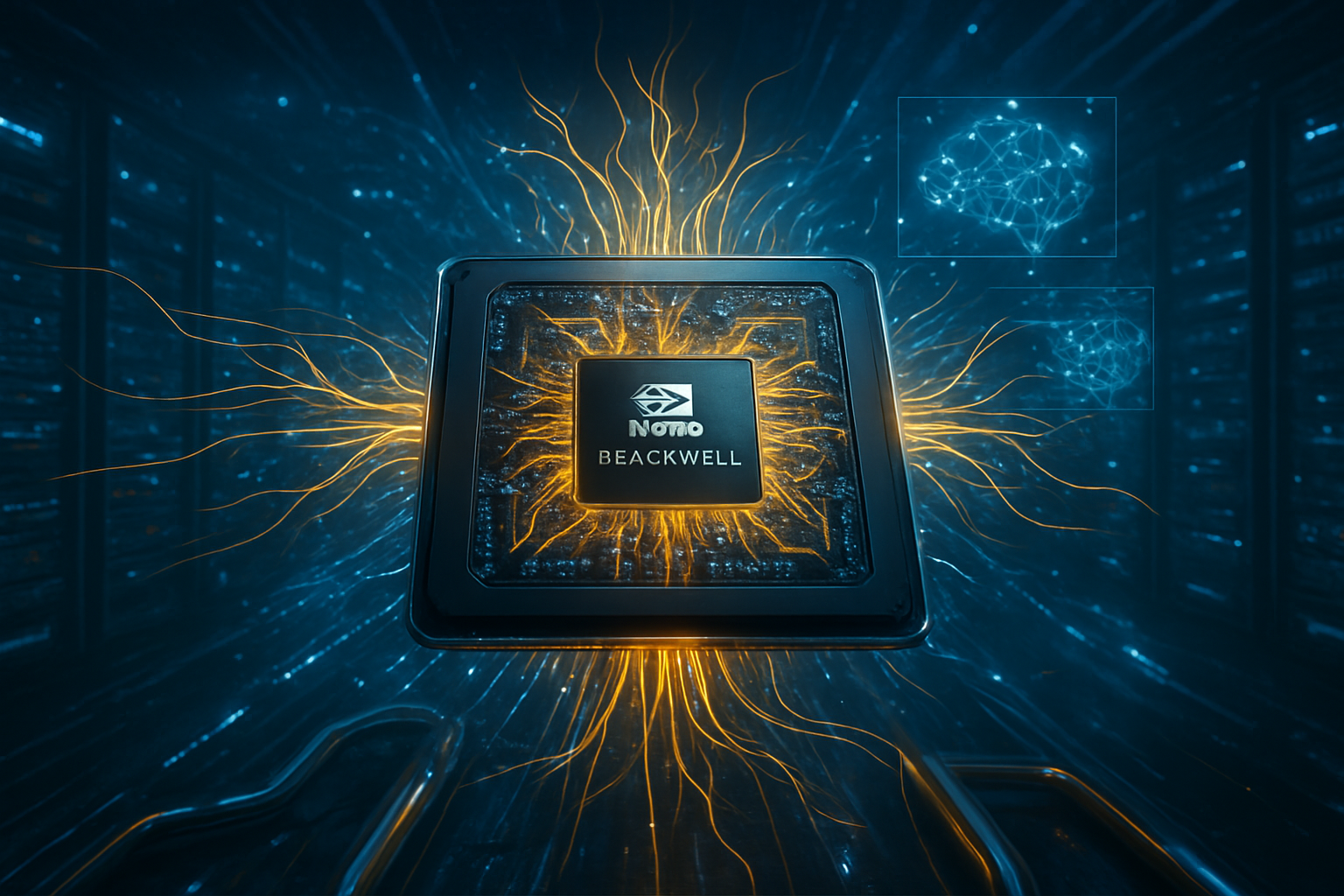
The rivalry between Intel Foundry and TSMC has entered a new phase. Intel has successfully "on-shored" the world's most advanced node (1.8nm) before TSMC has brought its 2nm technology to the U.S. (slated for 2027). This gives Intel a temporary "geographical leadership" in the most advanced domestic silicon, a point of pride for the "National Champion." However, TSMC’s superior yields and massive customer base, including Nvidia and AMD (NASDAQ: AMD), ensure it remains the volume leader. Nvidia has already begun producing Blackwell AI GPUs at TSMC Arizona, and reports suggest the company is exploring Intel’s 18A node for its next-generation consumer gaming GPUs to further diversify its manufacturing base.
The CHIPS Act funding structures also reflect these differing roles. In a landmark deal in August 2025, the U.S. government converted billions in grants into a 9.9% federal equity stake in Intel, providing the company with $11.1 billion in total support and the financial flexibility to focus on the 18A ramp. In contrast, TSMC has followed a more traditional milestone-based grant path, receiving $6.6 billion in direct grants as it hits production targets. This government involvement has effectively de-risked the "Silicon Desert" for private investors, leading to a surge in secondary investments from equipment giants like ASML (NASDAQ: ASML) and Applied Materials (NASDAQ: AMAT).
Geopolitics and the "Silicon Shield" Paradox
The wider significance of Arizona’s mega-fabs extends far beyond corporate profits. Geopolitically, these milestones represent a "dual base" strategy intended to reduce global reliance on the Taiwan Strait. While this move strengthens U.S. national security, it has created a "Silicon Shield" paradox. Some in Taipei worry that as the U.S. becomes more self-sufficient in chip production, the strategic necessity of defending Taiwan might diminish. To mitigate this, TSMC has maintained a "one-generation gap" policy, ensuring that its most cutting-edge "mother fabs" remain in Taiwan, even as Arizona’s capabilities rapidly catch up.
National security is further bolstered by the Secure Enclave program, a $3 billion Department of Defense initiative executed through Intel’s Arizona facilities. As of late 2025, Intel’s Ocotillo campus is the only site in the world capable of producing sub-2nm defense-grade chips in a secure, domestic environment. These chips are destined for F-35 fighter jets, advanced radar systems, and autonomous weapons, ensuring that the U.S. military’s most sensitive hardware is not subject to foreign supply chain disruptions.
However, the rapid industrialization of the desert has not come without concerns. The scale of manufacturing requires millions of gallons of water per day, forcing a radical evolution in water management. TSMC has implemented a 15-acre Industrial Water Reclamation Plant that recycles 90% of its process water, while Intel has achieved a "net-positive" water status through collaborative projects with the Gila River Indian Community. Despite these efforts, environmental groups remain watchful over the disposal of PFAS ("forever chemicals") and the massive energy load these fabs place on the Arizona grid—with a single fully expanded site consuming as much electricity as a small city.
The Roadmap to 2030: 1.6nm and the Talent Gap
Looking toward the end of the decade, the roadmap for the Silicon Desert is even more ambitious. Intel is already preparing for the introduction of Intel 14A (1.4nm) in 2026–2027, which will mark the first commercial use of High-NA EUV lithography scanners—the most complex machines ever built. TSMC has also accelerated its timeline, with ground already broken on Phase 3 of Fab 21, which is slated to produce 2nm (N2) and 1.6nm (A16) chips as early as 2027 to meet the insatiable demand for AI compute.
The most significant hurdle to this growth is not technology, but talent. A landmark study suggests a shortage of 67,000 workers in the U.S. semiconductor industry by 2030. Arizona alone requires an estimated 25,000 direct jobs to staff its expanding fabs. To address this, Arizona State University (ASU) has become the largest engineering school in the U.S., and new "Future 48" workforce accelerators have opened in 2025 to provide rapid, hands-on training for technicians. The ability of the region to fill these roles will determine whether the Silicon Desert can maintain its current momentum.
A New Chapter in Industrial History
The operational milestones reached by Intel and TSMC in late 2025 mark the end of the "beginning" for the U.S. semiconductor resurgence. The successful high-volume manufacturing of 18A and the record-breaking yields of 4nm production prove that the United States can still compete at the highest levels of industrial complexity. This development is perhaps the most significant milestone in semiconductor history since the invention of the integrated circuit, representing a fundamental rebalancing of global technological power.
In the coming months, the industry will be watching for the first consumer products powered by Arizona-made 18A chips and the continued expansion of the advanced packaging ecosystem. As the "Silicon Desert" continues to bloom, the focus will shift from building the fabs to sustaining them—ensuring the energy grid, the water supply, and the workforce can support a multi-decadal era of American silicon leadership.
This content is intended for informational purposes only and represents analysis of current AI developments.
TokenRing AI delivers enterprise-grade solutions for multi-agent AI workflow orchestration, AI-powered development tools, and seamless remote collaboration platforms.
For more information, visit https://www.tokenring.ai/.