In a definitive moment for the global semiconductor industry, Intel Corporation (NASDAQ: INTC) officially announced on December 19, 2025, that its cutting-edge 18A (1.8nm-class) process node has entered High-Volume Manufacturing (HVM). This milestone, achieved at the company’s flagship Fab 52 facility in Chandler, Arizona, represents the successful culmination of the "Five Nodes in Four Years" (5N4Y) roadmap—a daring strategy once viewed with skepticism by industry analysts. The transition to HVM signals that Intel has finally stabilized yields and is ready to challenge the dominance of Asian foundry giants.
The launch is headlined by the first retail shipments of "Panther Lake" processors, branded as the Core Ultra 300 series. These chips, which power a new generation of AI-native laptops from partners like Dell and HP, serve as the primary vehicle for Intel’s most advanced transistor technologies to date. By hitting this production target before the close of 2025, Intel has not only met its internal deadlines but has also leapfrogged competitors in key architectural innovations, most notably in power delivery and transistor structure.
The Architecture of Dominance: RibbonFET and PowerVia
The technical backbone of the 18A node rests on two revolutionary technologies: RibbonFET and PowerVia. RibbonFET is Intel’s implementation of Gate-All-Around (GAA) transistor architecture, which replaces the long-standing FinFET design. By surrounding the conducting channel on all four sides with the gate, RibbonFET provides superior electrostatic control, drastically reducing power leakage while increasing switching speeds. This allows for higher performance at lower voltages, a critical requirement for the thermally constrained environments of modern laptops and high-density data centers.
However, the true "secret sauce" of 18A is PowerVia, Intel’s proprietary backside power delivery system. Traditionally, power and signal lines are bundled together on the front of a silicon wafer, leading to "routing congestion" and voltage drops. PowerVia moves the power delivery network to the back of the wafer, separating it entirely from the signal lines. Technical data released during the HVM launch indicates that PowerVia reduces IR (voltage) droop by approximately 10% and enables a 6% to 10% frequency gain. Furthermore, by freeing up space on the front side, Intel has achieved a 30% increase in transistor density over its previous Intel 3 node, reaching an estimated 238 million transistors per square millimeter (MTr/mm²).
Initial reactions from the semiconductor research community have been overwhelmingly positive. Analysts note that while Taiwan Semiconductor Manufacturing Company (NYSE: TSM) still maintains a slight lead in raw transistor density with its N2 node, TSMC’s implementation of backside power is not expected until the N2P or A16 nodes in late 2026. This gives Intel a temporary but significant technical advantage in power efficiency—a metric that has become the primary battleground in the AI era.
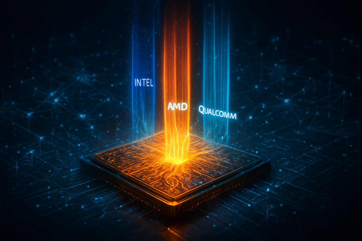
Reshaping the Foundry Landscape
The move to HVM for 18A is more than a technical victory; it is a strategic earthquake for the foundry market. Under the leadership of CEO Lip-Bu Tan, who took the helm in early 2025, Intel Foundry has been spun off into an independent subsidiary, a move that has successfully courted major tech giants. Microsoft (NASDAQ: MSFT) and Amazon (NASDAQ: AMZN) have already emerged as anchor customers, with Microsoft reportedly utilizing 18A for its "Maia 2" AI accelerators. Perhaps most surprisingly, NVIDIA (NASDAQ: NVDA) finalized a $5 billion strategic investment in Intel late this year, signaling a collaborative shift where the two companies are co-developing custom x86 CPUs for data center applications.
For years, the industry was a duopoly between TSMC and Samsung Electronics (KRX: 005930). However, Intel’s 18A yields—now stabilized between 60% and 65%—have allowed it to overtake Samsung, whose 2nm-class SF2 process has reportedly struggled with yield bottlenecks near the 40% mark. This positioning makes Intel the clear secondary alternative to TSMC for high-performance silicon. Even Apple (NASDAQ: AAPL), which has historically been exclusive to TSMC for its flagship chips, is reportedly evaluating Intel 18A for its lower-tier Mac and iPad silicon starting in 2027 to diversify its supply chain and mitigate geopolitical risks.
AI Integration and the Broader Silicon Landscape
The broader significance of the 18A launch lies in its optimization for Artificial Intelligence. The lead product, Panther Lake, features a next-generation Neural Processing Unit (NPU) capable of over 100 TOPS (Trillions of Operations Per Second). This is specifically architected to handle local generative AI workloads, such as real-time language translation and on-device image generation, without relying on cloud resources. The inclusion of the Xe3 "Celestial" graphics architecture further bolsters this, delivering a 50% improvement in integrated GPU performance over previous generations.
In the context of the global AI race, 18A provides the hardware foundation necessary for the next leap in "Agentic AI"—autonomous systems that require massive local compute power. This milestone echoes the historical significance of the move to 45nm and High-K Metal Gate technology in 2007, which cemented Intel's dominance for a decade. By successfully navigating the transition to GAA and backside power simultaneously, Intel has proven that the "IDM 2.0" strategy was not just a survival plan, but a roadmap to regaining industry leadership.
The Road to 14A and Beyond
Looking ahead, the HVM status of 18A is just the beginning. Intel has already begun installing "High-NA" (High Numerical Aperture) EUV lithography machines from ASML Holding (NASDAQ: ASML) for its upcoming 14A node. Near-term developments include the broad global launch of Panther Lake at CES 2026 and the ramp-up of "Clearwater Forest," a high-core-count server chip designed for the world’s largest data centers.
Experts predict that the next challenge will be scaling these innovations to the "Angstrom Era" (10A and beyond). While the 18A node has solved the immediate yield crisis, maintaining this momentum will require constant refinement of the High-NA EUV process and further advancements in 3D chip stacking (Foveros Direct). The industry will be watching closely to see if Intel can maintain its yield improvements as it moves toward 14A in 2027.
Conclusion: A New Chapter for Intel
The official launch of Intel 18A into high-volume manufacturing marks the most significant turnaround in the company's 57-year history. By successfully delivering RibbonFET and PowerVia, Intel has reclaimed its position at the leading edge of semiconductor manufacturing. The key takeaways are clear: Intel is no longer just a chipmaker, but a world-class foundry capable of serving the most demanding AI and hyperscale customers.
In the coming months, the focus will shift from manufacturing capability to market adoption. As Panther Lake laptops hit the shelves and Microsoft’s 18A-based AI chips enter the data center, the real-world performance of this silicon will be the ultimate test. For now, the "Silicon Throne" is once again a contested seat, and the competition between Intel and TSMC promises to drive an unprecedented era of innovation in AI hardware.
This content is intended for informational purposes only and represents analysis of current AI developments.
TokenRing AI delivers enterprise-grade solutions for multi-agent AI workflow orchestration, AI-powered development tools, and seamless remote collaboration platforms.
For more information, visit https://www.tokenring.ai/.