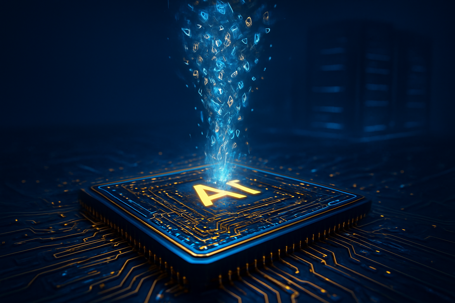
As we close out 2025, the artificial intelligence landscape looks radically different than it did just twelve months ago. While the year ended with the sophisticated agentic capabilities of GPT-5 and Llama 4, historians will likely point to January 2025 as the true inflection point. The catalyst was the release of DeepSeek R1, a reasoning model from a relatively lean Chinese startup that shattered the "compute moat" and proved that frontier-level intelligence could be achieved at a fraction of the cost previously thought necessary.
DeepSeek R1 didn't just match the performance of the world’s most expensive models on critical benchmarks; it did so using a training budget estimated at just $5.58 million. In an industry where Silicon Valley giants like Microsoft (NASDAQ: MSFT) and Alphabet (NASDAQ: GOOGL) were projecting capital expenditures in the hundreds of billions, DeepSeek’s efficiency was a systemic shock. It forced a global pivot from "brute-force scaling" to "algorithmic optimization," fundamentally changing how AI is built, funded, and deployed across the globe.
The Technical Breakthrough: GRPO and the Rise of "Inference-Time Scaling"
The technical brilliance of DeepSeek R1 lies in its departure from traditional reinforcement learning (RL) pipelines. Most frontier models rely on a "critic" model to provide feedback during the training process, a method that effectively doubles the necessary compute resources. DeepSeek introduced Group Relative Policy Optimization (GRPO), an algorithm that estimates a baseline by averaging the scores of a group of outputs rather than requiring a separate critic. This innovation, combined with a Mixture-of-Experts (MoE) architecture featuring 671 billion parameters (of which only 37 billion are active per token), allowed the model to achieve elite reasoning capabilities with unprecedented efficiency.
DeepSeek’s development path was equally unconventional. They first released "R1-Zero," a model trained through pure reinforcement learning with zero human supervision. While R1-Zero displayed remarkable "self-emergent" reasoning—including the ability to self-correct and "think" through complex problems—it suffered from poor readability and language-mixing. The final DeepSeek R1 addressed these issues by using a small "cold-start" dataset of high-quality reasoning traces to guide the RL process. This hybrid approach proved that a massive corpus of human-labeled data was no longer the only path to a "god-like" reasoning engine.
Perhaps the most significant technical contribution to the broader ecosystem was DeepSeek’s commitment to open-weight accessibility. Alongside the flagship model, the team released six distilled versions of R1, ranging from 1.5 billion to 70 billion parameters, based on architectures like Meta’s (NASDAQ: META) Llama and Alibaba’s Qwen. These distilled models allowed developers to run reasoning capabilities—previously restricted to massive data centers—on consumer-grade hardware. This democratization of "thinking tokens" sparked a wave of innovation in local, privacy-focused AI that defined much of the software development in late 2025.
Initial reactions from the AI research community were a mix of awe and skepticism. Critics initially questioned the $6 million figure, noting that total research and development costs were likely much higher. However, as independent labs replicated the results throughout the spring of 2025, the reality set in: DeepSeek had achieved in months what others spent years and billions to approach. The "DeepSeek Shockwave" was no longer a headline; it was a proven technical reality.
Market Disruption and the End of the "Compute Moat"
The financial markets' reaction to DeepSeek R1 was nothing short of historic. On what is now remembered as "DeepSeek Monday" (January 27, 2025), Nvidia (NASDAQ: NVDA) saw its stock plummet by 17%, wiping out roughly $600 billion in market value in a single day. Investors, who had bet on the idea that AI progress required an infinite supply of high-end GPUs, suddenly feared that DeepSeek’s efficiency would collapse the demand for massive hardware clusters. While Nvidia eventually recovered as the "Jevons Paradox" took hold—cheaper AI leading to vastly more AI usage—the event permanently altered the strategic playbook for Big Tech.
For major AI labs, DeepSeek R1 was a wake-up call that forced a re-evaluation of their "scaling laws." OpenAI, which had been the undisputed leader in reasoning with its o1-series, found itself under immense pressure to justify its massive burn rate. This pressure accelerated the development of GPT-5, which launched in August 2025. Rather than just being "bigger," GPT-5 leaned heavily into the efficiency lessons taught by R1, integrating "dynamic compute" to decide exactly how much "thinking time" a specific query required.
Startups and mid-sized tech companies were the primary beneficiaries of this shift. With the availability of R1’s distilled weights, companies like Amazon (NASDAQ: AMZN) and Salesforce (NYSE: CRM) were able to integrate sophisticated reasoning agents into their enterprise platforms without the prohibitive costs of proprietary API calls. The "reasoning layer" of the AI stack became a commodity almost overnight, shifting the competitive advantage from who had the smartest model to who had the most useful, integrated application.
The disruption also extended to the consumer space. By late January 2025, the DeepSeek app had surged to the top of the US iOS App Store, surpassing ChatGPT. It was a rare moment of a Chinese software product dominating the US market in a high-stakes technology sector. This forced Western companies to compete not just on capability, but on the speed and cost of their inference, leading to the "Inference Wars" of mid-2025 where token prices dropped by over 90% across the industry.
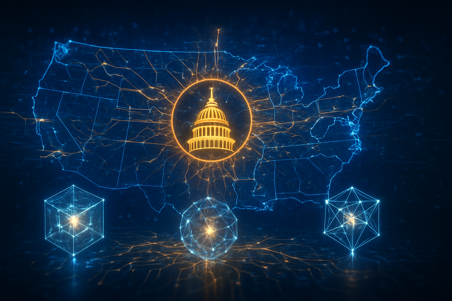
Geopolitics and the "Sputnik Moment" of Open-Weights
Beyond the technical and economic metrics, DeepSeek R1 carried immense geopolitical weight. Developed in Hangzhou using Nvidia H800 GPUs—chips specifically modified to comply with US export restrictions—the model proved that "crippled" hardware was not a definitive barrier to frontier-level AI. This sparked a fierce debate in Washington D.C. regarding the efficacy of chip bans and whether the "compute moat" was actually a porous border.
The release also intensified the "Open Weight" debate. By releasing the model weights under an MIT license, DeepSeek positioned itself as a champion of open-source, a move that many saw as a strategic play to undermine the proprietary advantages of US-based labs. This forced Meta to double down on its open-source strategy with Llama 4, and even led to the surprising "OpenAI GPT-OSS" release in September 2025. The world moved toward a bifurcated AI landscape: highly guarded proprietary models for the most sensitive tasks, and a robust, DeepSeek-influenced open ecosystem for everything else.
However, the "DeepSeek effect" also brought concerns regarding safety and alignment to the forefront. R1 was criticized for "baked-in" censorship, often refusing to engage with topics sensitive to the Chinese government. This highlighted the risk of "ideological alignment," where the fundamental reasoning processes of an AI could be tuned to specific political frameworks. As these models were distilled and integrated into global workflows, the question of whose values were being "reasoned" with became a central theme of international AI safety summits in late 2025.
Comparisons to the 1957 Sputnik launch are frequent among industry analysts. Just as Sputnik proved that the Soviet Union could match Western aerospace capabilities, DeepSeek R1 proved that a focused, efficient team could match the output of the world’s most well-funded labs. It ended the era of "AI Exceptionalism" for Silicon Valley and inaugurated a truly multipolar era of artificial intelligence.
The Future: From Reasoning to Autonomous Agents
Looking toward 2026, the legacy of DeepSeek R1 is visible in the shift toward "Agentic AI." Now that reasoning has become efficient and affordable, the industry has moved beyond simple chat interfaces. The "thinking" capability introduced by R1 is now being used to power autonomous agents that can manage complex, multi-day projects, from software engineering to scientific research, with minimal human intervention.
We expect the next twelve months to see the rise of "Edge Reasoning." Thanks to the distillation techniques pioneered during the R1 era, we are beginning to see the first smartphones and laptops capable of local, high-level reasoning without an internet connection. This will solve many of the latency and privacy concerns that have hindered enterprise adoption of AI. The challenge now shifts from "can it think?" to "can it act safely and reliably in the real world?"
Experts predict that the next major breakthrough will be in "Recursive Self-Improvement." With models now capable of generating their own high-quality reasoning traces—as R1 did with its RL-based training—we are entering a cycle where AI models are the primary trainers of the next generation. The bottleneck is no longer human data, but the algorithmic creativity required to set the right goals for these self-improving systems.
A New Chapter in AI History
DeepSeek R1 was more than just a model; it was a correction. It corrected the assumption that scale was the only path to intelligence and that the US held an unbreakable monopoly on frontier AI. In the grand timeline of artificial intelligence, 2025 will be remembered as the year the "Scaling Laws" were amended by the "Efficiency Laws."
The key takeaway for businesses and policymakers is that the barrier to entry for world-class AI is lower than ever, but the competition is significantly fiercer. The "DeepSeek Shock" proved that agility and algorithmic brilliance can outpace raw capital. As we move into 2026, the focus will remain on how these efficient reasoning engines are integrated into the fabric of the global economy.
In the coming weeks, watch for the release of "DeepSeek R2" and the subsequent response from the newly formed US AI Safety Consortium. The era of the "Trillion-Dollar Model" may not be over, but thanks to a $6 million breakthrough in early 2025, it is no longer the only game in town.
This content is intended for informational purposes only and represents analysis of current AI developments.
TokenRing AI delivers enterprise-grade solutions for multi-agent AI workflow orchestration, AI-powered development tools, and seamless remote collaboration platforms.
For more information, visit https://www.tokenring.ai/.