In a move that signals the end of the "wild west" era for synthetic media, New York Governor Kathy Hochul signed the Synthetic Performer Disclosure Law (S.8420-A / A.8887-B) on December 11, 2025. The legislation establishes the nation’s first comprehensive framework requiring advertisers to clearly label any synthetic human actors or AI-generated people used in commercial content. As the advertising world increasingly leans on generative AI to slash production costs, this law marks a pivotal shift toward consumer transparency, mandating that the line between human and machine be clearly drawn for the public.
The enactment of this law, coming just weeks before the close of 2025, serves as a direct response to the explosion of "hyper-realistic" AI avatars that have begun to populate social media feeds and television commercials. By requiring a "conspicuous disclosure," New York is setting a high bar for digital honesty, effectively forcing brands to admit when the smiling faces in their campaigns are the product of code rather than DNA.
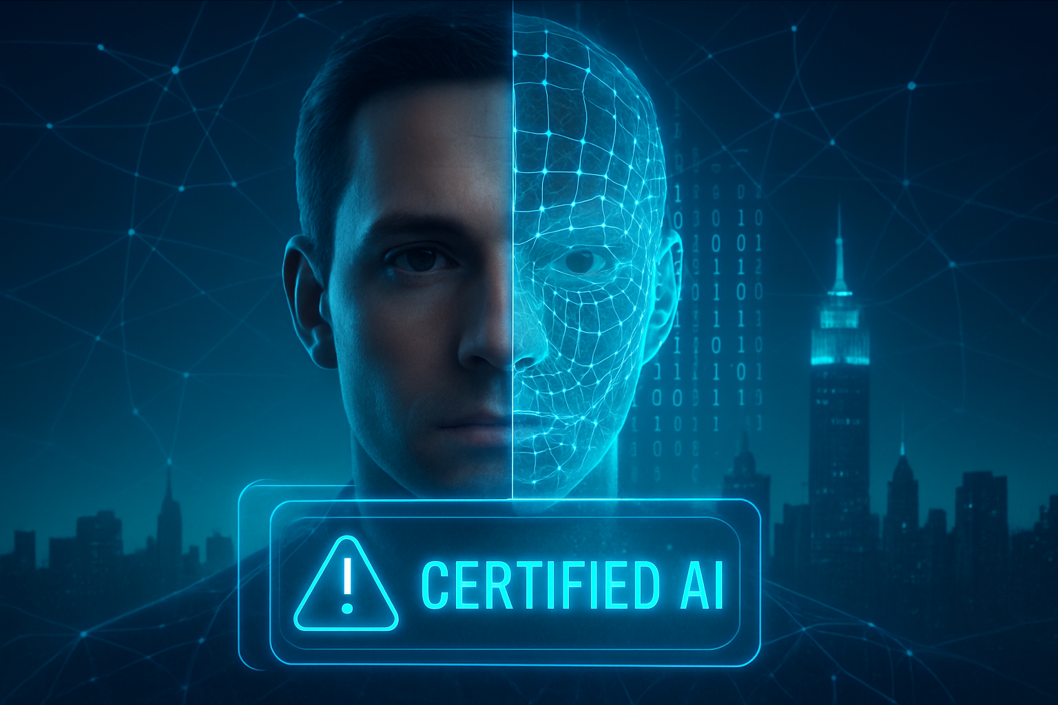
Defining the Synthetic Performer: The Technical Mandate
The new legislation specifically targets what it calls "synthetic performers"—digitally created assets generated by AI or software algorithms intended to create the impression of a real human being who is not recognizable as any specific natural person. Unlike previous "deepfake" laws that focused on the non-consensual use of real people's likenesses, this law addresses the "uncanny valley" of entirely fabricated humans. Under the new rules, any advertisement produced for commercial purposes must feature a label such as "AI-generated person" or "Includes synthetic performer" that is easily noticeable and understandable to the average consumer.
Technically, the law places the burden of "actual knowledge" on the content creator or sponsor. This means if a brand or an ad agency uses a platform like Synthesia or HeyGen to generate a spokesperson, they are legally obligated to disclose it. However, the law provides a safe harbor for media distributors; television networks and digital platforms like Meta (NASDAQ: META) or Alphabet (NASDAQ: GOOGL) are generally exempt from liability, provided they are not the primary creators of the content.
Industry experts note that this approach differs significantly from earlier, broader attempts at AI regulation. By focusing narrowly on "commercial purpose" and "synthetic performers," the law avoids infringing on artistic "expressive works" like movies, video games, or documentaries. This surgical precision has earned the law praise from the AI research community for protecting creative innovation while simultaneously providing a necessary "nutrition label" for commercial persuasion.
Shaking Up the Ad Industry: Meta, Google, and the Cost of Transparency
The business implications of the Synthetic Performer Disclosure Law are immediate and far-reaching. Major tech giants that provide AI-driven advertising tools, including Adobe (NASDAQ: ADBE) and Microsoft (NASDAQ: MSFT), are already moving to integrate automated labeling features into their creative suites to help clients comply. For these companies, the law presents a dual-edged sword: while it validates the utility of their AI tools, the requirement for a "conspicuous" label could potentially diminish the "magic" of AI-generated content that brands have used to achieve a seamless, high-end look on a budget.
For global advertising agencies like WPP (NYSE: WPP) and Publicis, the law necessitates a rigorous new compliance layer in the creative process. There is a growing concern that the "AI-generated" tag might carry a stigma, leading some brands to pull back from synthetic actors in favor of "authentic" human talent—a trend that would be a major win for labor unions. SAG-AFTRA, a primary advocate for the bill, hailed the signing as a landmark victory, arguing that it prevents AI from deceptively replacing human actors without the public's knowledge.
Startups specializing in AI avatars are also feeling the heat. While these companies have seen massive valuations based on their ability to produce "indistinguishable" human content, they must now pivot their marketing strategies. The strategic advantage may shift to companies that can provide "certified authentic" human content or those that develop the most aesthetically pleasing ways to incorporate disclosures without disrupting the viewer's experience.
A New Era for Digital Trust and the Broader AI Landscape
The New York law is a significant milestone in the broader AI landscape, mirroring the global trend toward "AI watermarking" and provenance standards like C2PA. It arrives at a time when public trust in digital media is at an all-time low, and the "AI-free" brand movement is gaining momentum among Gen Z and Millennial consumers. By codifying transparency, New York is effectively treating AI-generated humans as a new category of "claim" that must be substantiated, much like "organic" or "sugar-free" labels in the food industry.
However, the law has also sparked concerns about "disclosure fatigue." Some critics argue that as AI becomes ubiquitous in every stage of production—from color grading to background extras—labeling every synthetic element could lead to a cluttered and confusing visual landscape. Furthermore, the law enters a complex legal environment where federal authorities are also vying for control. The White House recently issued an Executive Order aiming for a national AI standard, creating a potential conflict with New York’s specific mandates.
Comparatively, this law is being viewed as the "GDPR moment" for synthetic media. Just as Europe’s data privacy laws forced a global rethink of digital tracking, New York’s disclosure requirements are expected to become the de facto national standard, as few brands will want to produce separate, non-labeled versions of ads for the rest of the country.
The Future of Synthetic Influence: What Comes Next?
Looking ahead, the "Synthetic Performer Disclosure Law" is likely just the first of many such regulations. Near-term developments are expected to include the expansion of these rules to "AI Influencers" on platforms like TikTok and Instagram, where the line between a real person and a synthetic avatar is often intentionally blurred. As AI actors become more interactive and capable of real-time engagement, the need for disclosure will only grow more acute.
Experts predict that the next major challenge will be enforcement in the decentralized world of social media. While large brands will likely comply to avoid the $5,000-per-violation penalties, small-scale creators and "shadow" advertisers may prove harder to regulate. Additionally, as generative AI moves into audio and real-time video calls, the definition of a "performer" will need to evolve. We may soon see "Transparency-as-a-Service" companies emerge, offering automated verification and labeling tools to ensure advertisements remain compliant across all 50 states.
The interplay between this law and the recently signed RAISE Act (Responsible AI Safety and Education Act) in New York also suggests a future where AI safety and consumer transparency are inextricably linked. The RAISE Act’s focus on "frontier" model safety protocols will likely provide the technical backend needed to track the provenance of the very avatars the disclosure law seeks to label.
Closing the Curtain on Deceptive AI
The enactment of New York’s AI Avatar Disclosure Law is a watershed moment for the 21st-century media landscape. By mandating that synthetic humans be identified, the state has taken a firm stand on the side of consumer protection and human labor. The key takeaway for the industry is clear: the era of passing off AI as human without consequence is over.
As the law takes effect in June 2026, the industry will be watching closely to see how consumers react to the "AI-generated" labels. Will it lead to a rejection of synthetic media, or will the public become desensitized to it? In the coming weeks and months, expect a flurry of activity from ad-tech firms and legal departments as they scramble to define what "conspicuous" truly means in a world where the virtual and the real are becoming increasingly difficult to distinguish.
This content is intended for informational purposes only and represents analysis of current AI developments.
TokenRing AI delivers enterprise-grade solutions for multi-agent AI workflow orchestration, AI-powered development tools, and seamless remote collaboration platforms.
For more information, visit https://www.tokenring.ai/.