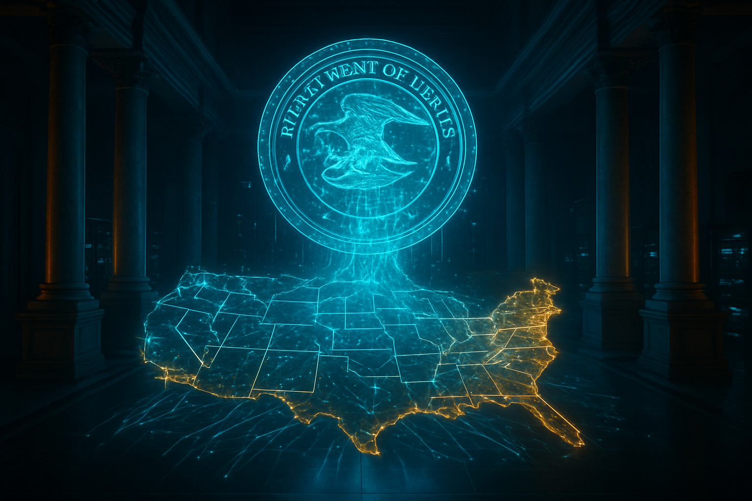
Blog

  • The Intelligence Revolution Moves Inward: How Edge AI Silicon is Reclaiming Privacy and Performance

    The Intelligence Revolution Moves Inward: How Edge AI Silicon is Reclaiming Privacy and Performance

    As we close out 2025, the center of gravity for artificial intelligence has undergone a seismic shift. For years, the narrative of AI progress was defined by massive, power-hungry data centers and the "cloud-first" approach that required every query to travel hundreds of miles to a server rack. However, the final quarter of 2025 has solidified a new era: the era of Edge AI. Driven by a new generation of specialized semiconductors, high-performance AI is no longer a remote service—it is a local utility living inside our smartphones, IoT sensors, and wearable devices.

    This transition represents more than just a technical milestone; it is a fundamental restructuring of the digital ecosystem. By moving the "brain" of the AI directly onto the device, manufacturers are solving the three greatest hurdles of the generative AI era: latency, privacy, and cost. With the recent launches of flagship silicon from industry titans and a regulatory environment increasingly favoring "privacy-by-design," the rise of Edge AI silicon is the defining tech story of the year.

    The Architecture of Autonomy: Inside the 2025 Silicon Breakthroughs

    The technical landscape of late 2025 is dominated by a new class of Neural Processing Units (NPUs) that have finally bridged the gap between mobile efficiency and server-grade performance. At the heart of this revolution is the Apple Inc. (NASDAQ: AAPL) A19 Pro chip, which debuted in the iPhone 17 Pro this past September. Unlike previous iterations, the A19 Pro features a 16-core Neural Engine and, for the first time, integrated neural accelerators within the GPU cores themselves. This "hybrid compute" architecture allows the device to run 8-billion-parameter models like Llama-3 with sub-second response times, enabling real-time "Visual Intelligence" that can analyze everything the camera sees without ever uploading a single frame to the cloud.

    Not to be outdone, Qualcomm Inc. (NASDAQ: QCOM) recently unveiled the Snapdragon 8 Elite Gen 5, a powerhouse that delivers an unprecedented 80 TOPS (Tera Operations Per Second) of AI performance. The chip’s second-generation Oryon CPU cores are specifically optimized for "agentic AI"—software that doesn't just answer questions but performs multi-step tasks across different apps locally. Meanwhile, MediaTek Inc. (TPE: 2454) has disrupted the mid-range market with its Dimensity 9500, the first mobile SoC to natively support BitNet 1.58-bit (ternary) model processing. This mathematical breakthrough allows for a 40% acceleration in model loading while reducing power consumption by a third, making high-end AI accessible on more affordable hardware.

    These advancements differ from previous approaches by moving away from general-purpose computing toward "Physical AI." While older chips treated AI as a secondary task, 2025’s silicon is built from the ground up to handle transformer-based networks and vision-language models (VLMs). Initial reactions from the research community, including experts at the AI Infra Summit in Santa Clara, suggest that the "pre-fill" speeds—the time it takes for an AI to understand a prompt—have improved by nearly 300% year-over-year, effectively killing the "loading" spinner that once plagued mobile AI.

    Strategic Realignment: The Battle for the Edge

    The rise of specialized Edge silicon is forcing a massive strategic pivot among tech giants. For NVIDIA Corporation (NASDAQ: NVDA), the focus has expanded from the data center to the "personal supercomputer." Their new Project Digits platform, powered by the Blackwell-based GB10 Grace Blackwell Superchip, allows developers to run 200-billion-parameter models locally. By providing the hardware for "Sovereign AI," NVIDIA is positioning itself as the infrastructure provider for enterprises that are too privacy-conscious to use public clouds.

    The competitive implications are stark. Traditional cloud providers like Alphabet Inc. (NASDAQ: GOOGL) and Microsoft Corporation (NASDAQ: MSFT) are now in a race to vertically integrate. Google’s Tensor G5, manufactured by Taiwan Semiconductor Manufacturing Company (NYSE: TSM) on its refined 3nm process, is a direct attempt to decouple Pixel's AI features from the Google Cloud, ensuring that Gemini Nano can function in "Airplane Mode." This shift threatens the traditional SaaS (Software as a Service) model; if the device in your pocket can handle the compute, the need for expensive monthly AI subscriptions may begin to evaporate, forcing companies to find new ways to monetize the "intelligence" they provide.

    Startups are also finding fertile ground in this new hardware reality. Companies like Hailo and Tenstorrent (led by legendary architect Jim Keller) are licensing RISC-V based AI IP, allowing niche manufacturers to build custom silicon for everything from smart mirrors to industrial robots. This democratization of high-performance silicon is breaking the duopoly of ARM and x86, leading to a more fragmented but highly specialized hardware market.

    Privacy, Policy, and the Death of Latency

    The broader significance of Edge AI lies in its ability to resolve the "Privacy Paradox." Until now, users had to choose between the power of large-scale AI and the security of their personal data. With the 2025 shift, "Local RAG" (Retrieval-Augmented Generation) has become the standard. This allows a device to index a user’s entire digital life—emails, photos, and health data—locally, providing a hyper-personalized AI experience that never leaves the device.

    This hardware-led privacy has caught the eye of regulators. On December 11, 2025, the US administration issued a landmark Executive Order on National AI Policy, which explicitly encourages "privacy-by-design" through on-device processing. Similarly, the European Union's recent "Digital Omnibus" package has shown a willingness to loosen certain data-sharing restrictions for companies that utilize local inference, recognizing it as a superior method for protecting citizen data. This alignment of hardware capability and government policy is accelerating the adoption of AI in sensitive sectors like healthcare and defense.

    Comparatively, this milestone is being viewed as the "Broadband Moment" for AI. Just as the transition from dial-up to broadband enabled the modern web, the transition from cloud-AI to Edge-AI is enabling "ambient intelligence." We are moving away from a world where we "use" AI to a world where AI is a constant, invisible layer of our physical environment, operating with sub-50ms latency that feels instantaneous to the human brain.

    The Horizon: From Smartphones to Humanoids

    Looking ahead to 2026, the trajectory of Edge AI silicon points toward even deeper integration into the physical world. We are already seeing the first wave of "AI-enabled sensors" from Sony Group Corporation (NYSE: SONY) and STMicroelectronics N.V. (NYSE: STM). These sensors don't just capture images or motion; they perform inference within the sensor housing itself, outputting only metadata. This "intelligence at the source" will be critical for the next generation of AR glasses, which require extreme power efficiency to maintain a lightweight form factor.

    Furthermore, the "Physical AI" tier is set to explode. NVIDIA's Jetson AGX Thor, designed for humanoid robots, is now entering mass production. Experts predict that the lessons learned from mobile NPU efficiency will directly translate to more capable, longer-lasting autonomous robots. The challenge remains in the "memory wall"—the difficulty of moving data fast enough between memory and the processor—but advancements in HBM4 (High Bandwidth Memory) and analog-in-memory computing from startups like Syntiant are expected to address these bottlenecks by late 2026.

    A New Chapter in the Silicon Sagas

    The rise of Edge AI silicon in 2025 marks the end of the "Cloud-Only" era of artificial intelligence. By successfully shrinking the immense power of LLMs into pocket-sized form factors, the semiconductor industry has delivered on the promise of truly personal, private, and portable intelligence. The key takeaways are clear: hardware is once again the primary driver of software innovation, and privacy is becoming a feature of the silicon itself, rather than just a policy on a website.

    As we move into 2026, the industry will be watching for the first "Edge-native" applications that can do things cloud AI never could—such as real-time, offline translation of complex technical jargon or autonomous drone navigation in GPS-denied environments. The intelligence revolution has moved inward, and the devices we carry are no longer just windows into a digital world; they are the architects of it.


    This content is intended for informational purposes only and represents analysis of current AI developments.

    TokenRing AI delivers enterprise-grade solutions for multi-agent AI workflow orchestration, AI-powered development tools, and seamless remote collaboration platforms.
    For more information, visit https://www.tokenring.ai/.

  • Silicon Diplomacy: How TSMC’s Global Triad is Redrawing the Map of AI Power

    Silicon Diplomacy: How TSMC’s Global Triad is Redrawing the Map of AI Power

    As of December 19, 2025, the global semiconductor landscape has undergone its most radical transformation since the invention of the integrated circuit. Taiwan Semiconductor Manufacturing Company (NYSE:TSM), long the sole guardian of the world’s most advanced "Silicon Shield," has successfully metastasized into a global triad of manufacturing power. With its massive facilities in Arizona, Japan, and Germany now either fully operational or nearing completion, the company has effectively decentralized the production of the world’s most critical resource: the high-performance AI chips that fuel everything from generative large language models to autonomous defense systems.

    This expansion marks a pivot from "efficiency-first" to "resilience-first" economics. The immediate significance of TSMC’s international footprint is twofold: it provides a geographical hedge against geopolitical tensions in the Taiwan Strait and creates a localized supply chain for the world's most valuable tech giants. By late 2025, the "Made in USA" and "Made in Japan" labels on high-end silicon are no longer aspirations—they are a reality that is fundamentally reshaping how AI companies calculate risk and roadmap their future hardware.

    The Yield Surprise: Arizona and the New Technical Standard

    The most significant technical milestone of 2025 has been the performance of TSMC’s Fab 1 in Phoenix, Arizona. Initially plagued by labor disputes and cultural friction during its construction phase, the facility has silenced critics by achieving 4nm and 5nm yield rates that are approximately 4 percentage points higher than equivalent fabs in Taiwan, reaching a staggering 92%. This technical feat is largely attributed to the implementation of "Digital Twin" manufacturing technology, where every process in the Arizona fab is mirrored and optimized in a virtual environment before execution, combined with a highly automated workforce model that mitigated early staffing challenges.

    While Arizona focuses on the cutting-edge 4nm and 3nm nodes (with 2nm production accelerated for 2027), the Japanese and German expansions serve different but equally vital technical roles. In Kumamoto, Japan, the JASM (Japan Advanced Semiconductor Manufacturing) facility has successfully ramped up 12nm to 28nm production, providing the specialized logic required for image sensors and automotive AI. Meanwhile, the ESMC (European Semiconductor Manufacturing Company) in Dresden, Germany, has broken ground on a facility dedicated to 16nm and 28nm "specialty" nodes. These are not the flashy chips that power ChatGPT, but they are the essential "glue" for the industrial and automotive AI sectors that keep Europe’s economy moving.

    Perhaps the most critical technical development of late 2025 is the expansion of advanced packaging. AI chips like NVIDIA’s (NASDAQ:NVDA) Blackwell and upcoming Rubin platforms rely on CoWoS (Chip-on-Wafer-on-Substrate) packaging to function. To support its international fabs, TSMC has entered a landmark partnership with Amkor Technology (NASDAQ:AMKR) in Peoria, Arizona, to provide "turnkey" advanced packaging services. This ensures that a chip can be fabricated, packaged, and tested entirely on U.S. soil—a first for the high-end AI industry.

    Initial reactions from the AI research and engineering communities have been overwhelmingly positive. Hardware architects at major labs note that the proximity of these fabs to U.S.-based design centers allows for faster "tape-out" cycles and reduced latency in the prototyping phase. The technical success of the Arizona site, in particular, has validated the theory that leading-edge manufacturing can indeed be successfully exported from Taiwan if supported by sufficient capital and automation.

    The AI Titans and the "US-Made" Premium

    The primary beneficiaries of TSMC’s global expansion are the "Big Three" of AI hardware: Apple (NASDAQ:AAPL), NVIDIA, and AMD (NASDAQ:AMD). For these companies, the international fabs represent more than just extra capacity; they offer a strategic advantage in a world where "sovereign AI" is becoming a requirement for government contracts. Apple, as TSMC’s anchor customer in Arizona, has already transitioned its A16 Bionic and M-series chips to the Phoenix site, ensuring that the hardware powering the next generation of iPhones and Macs is shielded from Pacific supply chain shocks.

    NVIDIA has similarly embraced the shift, with CEO Jensen Huang confirming that the company is willing to pay a "fair price" for Arizona-made wafers, despite a reported 20–30% markup over Taiwan-based production. This price premium is being treated as an insurance policy. By securing 3nm and 2nm capacity in the U.S. for its future "Rubin" GPU architecture, NVIDIA is positioning itself as the only AI chip provider capable of meeting the strict domestic-sourcing requirements of the U.S. Department of Defense and major federal agencies.

    However, this expansion also creates a new competitive divide. Startups and smaller AI labs may find themselves priced out of the "local" silicon market, forced to rely on older nodes or Taiwan-based production while the giants monopolize the secure, domestic capacity. This could lead to a two-tier AI ecosystem: one where "Premium AI" is powered by domestically-produced, secure silicon, and "Standard AI" relies on the traditional, more vulnerable global supply chain.

    Intel (NASDAQ:INTC) also faces a complicated landscape. While TSMC’s expansion validates the importance of U.S. manufacturing, it also introduces a formidable competitor on Intel’s home turf. As TSMC moves toward 2nm production in Arizona by 2027, the pressure on Intel Foundry to deliver on its 18A process node has never been higher. The market positioning has shifted: TSMC is no longer just a foreign supplier; it is a domestic powerhouse competing for the same CHIPS Act subsidies and talent pool as American-born firms.

    Silicon Shield 2.0: The Geopolitics of Redundancy

    The wider significance of TSMC’s global footprint lies in the evolution of the "Silicon Shield." For decades, the world’s dependence on Taiwan for advanced chips was seen as a deterrent against conflict. In late 2025, that shield is being replaced by "Geographic Redundancy." This shift is heavily incentivized by government intervention, including the $6.6 billion in grants awarded to TSMC under the U.S. CHIPS Act and the €5 billion in German state aid approved under the EU Chips Act.

    This "Silicon Diplomacy" has not been without its friction. The "Trump Factor" remains a significant variable in late 2025, with potential tariffs on Taiwanese-designed chips and a more transactional approach to defense treaties causing TSMC to accelerate its U.S. investments as a form of political appeasement. By building three fabs in Arizona instead of the originally planned two, TSMC is effectively buying political goodwill and ensuring its survival regardless of the administration in Washington.

    In Japan, the expansion has been dubbed the "Kumamoto Miracle." Unlike the labor struggles seen in the U.S., the Japanese government, along with partners like Sony (NYSE:SONY) and Toyota, has created a seamless integration of TSMC into the local economy. This has sparked a "semiconductor renaissance" in Japan, with the country once again becoming a hub for high-tech manufacturing. The geopolitical impact is clear: a new "democratic chip alliance" is forming between the U.S., Japan, and the EU, designed to isolate and outpace rival technological spheres.

    Comparisons to previous milestones, such as the rise of the Japanese memory chip industry in the 1980s, fall short of the current scale. We are witnessing the first time in history that the most advanced manufacturing technology is being distributed globally in real-time, rather than trickling down over decades. This ensures that even in the event of a regional crisis, the global AI engine—the most important economic driver of the 21st century—will not grind to a halt.

    The Road to 2nm and Beyond

    Looking ahead, the next 24 to 36 months will be defined by the race to 2nm and the integration of "A16" (1.6nm) angstrom-class nodes. TSMC has already signaled that its third Arizona fab, scheduled for the end of the decade, will likely be the first outside Taiwan to house these sub-2nm technologies. This suggests that the "technology gap" between Taiwan and its international satellites is rapidly closing, with the U.S. and Japan potentially reaching parity with Taiwan’s leading edge by 2028.

    We also expect to see a surge in "Silicon-as-a-Service" models, where TSMC’s regional hubs provide specialized, low-volume runs for local AI startups, particularly in the robotics and edge-computing sectors. The challenge will be the continued scarcity of specialized talent. While automation has solved some labor issues, the demand for PhD-level semiconductor engineers in Phoenix and Dresden is expected to outstrip supply for the foreseeable future, potentially leading to a "talent war" between TSMC, Intel, and Samsung.

    Experts predict that the next phase of expansion will move toward the "Global South," with preliminary discussions already underway for assembly and testing facilities in India and Vietnam. However, for the high-end AI chips that define the current era, the "Triad" of the U.S., Japan, and Germany will remain the dominant centers of power outside of Taiwan.

    A New Era for the AI Supply Chain

    The global expansion of TSMC is more than a corporate growth strategy; it is the fundamental re-architecting of the digital world's foundation. By late 2025, the company has successfully transitioned from a Taiwanese national champion to a global utility. The key takeaways are clear: yield rates in international fabs can match or exceed those in Taiwan, the AI industry is willing to pay a premium for localized security, and the "Silicon Shield" has been successfully decentralized.

    This development marks a definitive end to the "Taiwan-only" era of advanced computing. While Taiwan remains the R&D heart of TSMC, the muscle of the company is now distributed across the globe, providing a level of supply chain stability that was unthinkable just five years ago. This stability is the "hidden fuel" that will allow the AI revolution to continue its exponential growth, regardless of the geopolitical storms that may gather.

    In the coming months, watch for the first 3nm trial runs in Arizona and the potential announcement of a "Fab 3" in Japan. These will be the markers of a world where silicon is no longer a distant resource, but a local, strategic asset available to the architects of the AI future.


    This content is intended for informational purposes only and represents analysis of current AI and semiconductor developments as of December 2025.

    TokenRing AI delivers enterprise-grade solutions for multi-agent AI workflow orchestration, AI-powered development tools, and seamless remote collaboration platforms. For more information, visit https://www.tokenring.ai/.

  • Intel’s 18A Era: The Billion-Dollar Bet to Reclaim the Silicon Throne

    Intel’s 18A Era: The Billion-Dollar Bet to Reclaim the Silicon Throne

    As of December 19, 2025, the semiconductor landscape has reached a historic turning point. Intel (NASDAQ: INTC) has officially entered high-volume manufacturing (HVM) for its 18A process node, the 1.8nm-class technology that serves as the cornerstone of its "IDM 2.0" strategy. After years of trailing behind Asian rivals, the launch of 18A marks the completion of the ambitious "five nodes in four years" roadmap, signaling Intel’s return to the leading edge of transistor density and power efficiency. This milestone is not just a technical victory; it is a geopolitical statement, as the first major 2nm-class node to be manufactured on American soil begins to power the next generation of artificial intelligence and high-performance computing.

    The immediate significance of 18A lies in its role as the engine for Intel’s Foundry Services (IFS). By securing high-profile "anchor" customers like Microsoft (NASDAQ: MSFT) and Amazon (NASDAQ: AMZN), Intel has demonstrated that its manufacturing arm can compete for the world’s most demanding silicon designs. With the U.S. government now holding a 9.9% equity stake in the company via the CHIPS Act’s "Secure Enclave" program, 18A has become the de facto standard for domestic, secure microelectronics. As the industry watches the first 18A-powered "Panther Lake" laptops hit retail shelves this month, the question is no longer whether Intel can catch up, but whether it can sustain this lead against a fierce counter-offensive from TSMC and Samsung.

    The Technical "One-Two Punch": RibbonFET and PowerVia

    The 18A node represents the most significant architectural shift in Intel’s history since the introduction of FinFET over a decade ago. At its core are two revolutionary technologies: RibbonFET and PowerVia. RibbonFET is Intel’s implementation of Gate-All-Around (GAA) transistors, which replace the traditional fin-shaped channel with vertically stacked ribbons. This allows for precise control over the electrical current, drastically reducing leakage and enabling higher performance at lower voltages. While competitors like Samsung (KRX: 005930) have experimented with GAA earlier, Intel’s 18A implementation is optimized for the high-clock-speed demands of data center and enthusiast-grade processors.

    Complementing RibbonFET is PowerVia, an industry-first backside power delivery system. Traditionally, power and signal lines are bundled together on the front of the silicon wafer, leading to "routing congestion" that limits performance. PowerVia moves the power delivery to the back of the wafer, separating it from the signal lines. This technical decoupling has yielded a 15–18% improvement in performance-per-watt and a 30% increase in logic density. Crucially, Intel has successfully deployed PowerVia ahead of TSMC (NYSE: TSM), whose N2 process—while highly efficient—will not feature backside power until the subsequent A16 node.

    Initial reactions from the semiconductor research community have been cautiously optimistic. Analysts note that while Intel has achieved a "feature lead" by shipping backside power first, the ultimate test remains yield consistency. Early reports from Fab 52 in Arizona suggest that 18A yields are stabilizing, though they still trail the legendary maturity of TSMC’s N3 and N2 lines. However, the technical specifications of 18A—particularly its ability to drive high-current AI workloads with minimal heat soak—have positioned it as a formidable challenger to the status quo.

    A New Power Dynamic in the Foundry Market

    The successful ramp of 18A has sent shockwaves through the foundry ecosystem, directly challenging the dominance of TSMC. For the first time in years, major fabless companies have a viable "Plan B" for leading-edge manufacturing. Microsoft has already confirmed that its Maia 2 AI accelerators are being built on the 18A-P variant, seeking to insulate its Azure AI infrastructure from geopolitical volatility in the Taiwan Strait. Similarly, Amazon Web Services (AWS) is utilizing 18A for a custom AI fabric chip, highlighting a shift where tech giants are increasingly diversifying their supply chains away from a single-source model.

    This development places immense pressure on NVIDIA (NASDAQ: NVDA) and Apple (NASDAQ: AAPL). While Apple remains TSMC’s most pampered customer, the availability of a high-performance 1.8nm node in the United States offers a strategic hedge that was previously non-existent. For NVIDIA, which is currently grappling with insatiable demand for its Blackwell and upcoming Rubin architectures, Intel’s 18A represents a potential future manufacturing partner that could alleviate the persistent supply constraints at TSMC. The competitive implications are clear: TSMC can no longer dictate terms and pricing with the same absolute authority it held during the 5nm and 3nm eras.

    Furthermore, the emergence of 18A disrupts the mid-tier foundry market. As Intel migrates its internal high-volume products to 18A, it frees up capacity on its Intel 3 and Intel 4 nodes for "value-tier" foundry customers. This creates a cascading effect where older, but still advanced, nodes become more accessible to startups and automotive chipmakers. Samsung, meanwhile, has found itself squeezed between Intel’s technical aggression and TSMC’s yield reliability, forcing the South Korean giant to pivot toward specialized AI and automotive ASICs to maintain its market share.

    Geopolitics and the AI Infrastructure Race

    Beyond the balance sheets, 18A is a linchpin in the broader global trend of "silicon nationalism." As AI becomes the defining technology of the decade, the ability to manufacture the chips that power it has become a matter of national security. The U.S. government’s $8.9 billion equity stake in Intel, finalized in August 2025, underscores the belief that a leading-edge domestic foundry is essential. 18A is the first node to meet the "Secure Enclave" requirements, ensuring that sensitive defense and intelligence AI models are running on hardware that is both cutting-edge and domestically produced.

    The timing of the 18A rollout coincides with a massive expansion in AI data center construction. The node’s PowerVia technology is particularly well-suited for the "power wall" problem facing modern AI clusters. By delivering power more efficiently to the transistor level, 18A-based chips can theoretically run at higher sustained frequencies without the thermal throttling that plagues current-generation AI hardware. This makes 18A a critical component of the global AI landscape, potentially lowering the total cost of ownership for the massive LLM (Large Language Model) training runs that define the current era.

    However, this transition is not without concerns. The departure of long-time CEO Pat Gelsinger in early 2025 and the subsequent appointment of Lip-Bu Tan brought a shift in focus toward "profitability over pride." While 18A is a technical triumph, the market remains wary of Intel’s ability to transition from a "product-first" company to a "service-first" foundry. The complexity of 18A also requires advanced packaging techniques like Foveros Direct, which remain a bottleneck in the supply chain. If Intel cannot scale its packaging capacity as quickly as its wafer starts, the 18A advantage may be blunted by back-end delays.

    The Road to 14A and High-NA EUV

    Looking ahead, the 18A node is merely a stepping stone to Intel’s next major frontier: the 14A process. Scheduled for 2026–2027, 14A will be the first node to fully utilize High-NA (Numerical Aperture) EUV lithography machines from ASML (NASDAQ: ASML). Intel has already taken delivery of the first of these $380 million machines, giving it a head start in learning the complexities of next-generation patterning. The goal for 14A is to further refine the RibbonFET architecture and introduce even more aggressive scaling, potentially reclaiming the title of "unquestioned density leader" from TSMC.

    In the near term, the industry is watching the rollout of "Clearwater Forest," Intel’s 18A-based Xeon processor. Expected to ship in volume in the first half of 2026, Clearwater Forest will be the ultimate test of 18A’s viability in the lucrative server market. If it can outperform AMD (NASDAQ: AMD) in energy efficiency—a metric where Intel has struggled for years—it will signal a true renaissance for the company’s data center business. Additionally, we expect to see the first "Foundry-only" chips from smaller AI labs emerge on 18A by late 2026, as Intel’s design kits become more mature and accessible.

    The challenges remain formidable. Retooling a global giant while spinning off the foundry business into an independent subsidiary is a "change-the-engines-while-flying" maneuver. Experts predict that the next 18 months will be defined by "yield wars," where Intel must prove it can match TSMC’s 90%+ defect-free rates on mature nodes. If Intel hits its yield targets, 18A will be remembered as the moment the semiconductor world returned to a multi-polar reality.

    A New Chapter for Silicon

    In summary, the arrival of Intel 18A in late 2025 is more than just a successful product launch; it is the culmination of a decade-long struggle to fix a broken manufacturing engine. By delivering RibbonFET and PowerVia ahead of its primary competitors, Intel has regained the technical initiative. The "5 nodes in 4 years" journey has ended, and the era of "Intel Foundry" has truly begun. The strategic partnerships with Microsoft and the U.S. government provide a stable foundation, but the long-term success of the node will depend on its ability to attract a broader range of customers who have historically defaulted to TSMC.

    As we look toward 2026, the significance of 18A in AI history is clear. It provides the physical infrastructure necessary to sustain the current pace of AI innovation while offering a geographically diverse supply chain that mitigates global risk. For investors and tech enthusiasts alike, the coming months will be a period of intense scrutiny. Watch for the first third-party benchmarks of Panther Lake and the initial yield disclosures in Intel’s Q1 2026 earnings report. The silicon throne is currently contested, and for the first time in a long time, the outcome is anything but certain.


    This content is intended for informational purposes only and represents analysis of current semiconductor and AI developments.

    TokenRing AI delivers enterprise-grade solutions for multi-agent AI workflow orchestration, AI-powered development tools, and seamless remote collaboration platforms.
    For more information, visit https://www.tokenring.ai/.

  • Powering the Future: onsemi Navigates a Pivotal Shift in the EV and Industrial Semiconductor Landscape

    Powering the Future: onsemi Navigates a Pivotal Shift in the EV and Industrial Semiconductor Landscape

    As of December 19, 2025, ON Semiconductor (NASDAQ: ON), commonly known as onsemi, finds itself at a critical juncture in the global semiconductor market. After navigating a challenging 2024 and a transitional 2025, the company is emerging as a stabilizing leader in the power semiconductor space. While the broader automotive and industrial sectors have faced a prolonged "inventory digestion" phase, onsemi's strategic pivot toward high-growth AI data center power solutions and its aggressive vertical integration in Silicon Carbide (SiC) have caught the attention of Wall Street analysts.

    The immediate significance of onsemi’s current position lies in its resilience. Despite a cyclical downturn that saw revenue contract year-over-year, the company has maintained steady gross margins in the high 30% range and recently authorized a massive $6 billion share repurchase program. This move, combined with a flurry of analyst price target adjustments, signals a growing confidence that the company has reached its "trough" and is poised for a significant recovery as it scales its next-generation 200mm SiC manufacturing capabilities.

    Technical Milestones and the 200mm SiC Transition

    The technical narrative for onsemi in late 2025 is dominated by the transition from 150mm to 200mm (8-inch) Silicon Carbide wafers. This shift is not merely a change in size but a fundamental leap in manufacturing efficiency and cost-competitiveness. By moving to larger wafers, onsemi expects to significantly increase the number of chips per wafer, effectively lowering the cost of high-voltage power semiconductors essential for 800V electric vehicle (EV) architectures. The company has confirmed it is on track to begin generating meaningful revenue from 200mm production in early 2026, a milestone that industry experts view as a prerequisite for maintaining its roughly 24% share of the global SiC market.

    In addition to SiC, onsemi has made significant strides in its Field Stop 7 (FS7) IGBT technology. These devices are designed for high-power industrial applications, including solar inverters and energy storage systems. The FS7 platform offers lower switching losses and higher power density compared to previous generations, allowing for more compact and efficient energy infrastructure. Initial reactions from the industrial research community have been positive, noting that these advancements are crucial for the global transition toward renewable energy grids that require robust, high-efficiency power management.

    Furthermore, onsemi’s "Fab Right" strategy—a multi-year effort to consolidate manufacturing into fewer, more efficient, vertically integrated sites—is beginning to pay technical dividends. By controlling the entire supply chain from substrate growth to final module assembly, the company has achieved a level of quality control and supply assurance that few competitors can match. This vertical integration is particularly critical in the SiC market, where material scarcity and processing complexity have historically been major bottlenecks.

    Competitive Dynamics and the AI Data Center Pivot

    While the EV market has seen a slower-than-expected recovery in North America and Europe throughout 2025, onsemi has successfully offset this weakness by aggressively entering the AI data center market. In a landmark collaboration announced earlier this year with NVIDIA (NASDAQ: NVDA), onsemi is now supporting 800VDC power architectures for next-generation AI server racks. These high-voltage systems are designed to minimize energy loss as power moves from the grid to the GPU, a critical factor for data centers that are increasingly constrained by power availability and cooling costs.

    This pivot has placed onsemi in direct competition with other power giants like STMicroelectronics (NYSE: STM) and Infineon Technologies (OTCMKTS: IFNNY). While STMicroelectronics currently leads the SiC market by a small margin, onsemi’s recent deal with GlobalFoundries (NASDAQ: GFS) to develop 650V Gallium Nitride (GaN) power devices suggests a broadening of its portfolio. GaN technology is particularly suited for the ultra-compact power supply units (PSUs) used in AI servers, providing a complementary offering to its high-voltage SiC products.

    The competitive landscape is also being reshaped by onsemi’s focus on the Chinese EV market. Despite geopolitical tensions, onsemi has secured several major design wins with leading Chinese OEMs who are leading the charge in 800V vehicle adoption. By positioning itself as a key supplier for the most technologically advanced vehicles, onsemi is creating a strategic moat that protects its market share against lower-cost competitors who lack the high-voltage expertise and integrated supply chain of the Arizona-based firm.

    Wider Significance for the AI and Energy Landscape

    The evolution of onsemi reflects a broader trend in the technology sector: the convergence of AI and energy efficiency. As AI models become more computationally intensive, the demand for sophisticated power management has shifted from a niche industrial concern to a primary driver of the semiconductor industry. onsemi’s ability to double its AI-related revenue year-over-year in 2025 highlights how critical power semiconductors have become to the "AI Gold Rush." Without the efficiency gains provided by SiC and GaN, the energy requirements of modern data centers would be unsustainable.

    This development also underscores the changing nature of the EV market. The "hype phase" of 2021-2023 has given way to a more mature, performance-oriented market where efficiency is the primary differentiator. onsemi’s focus on 800V systems aligns with the industry’s shift toward faster charging and longer range, proving that the underlying technology is still advancing even if consumer adoption rates have hit a temporary plateau.

    However, the path forward is not without concerns. Analysts have pointed to the risks of overcapacity as onsemi, Wolfspeed (NYSE: WOLF), and others all race to bring massive SiC manufacturing hubs online. The Czech Republic hub and the expansion in Korea represent multi-billion-dollar bets that demand will eventually catch up with supply. If the EV recovery stalls further or if AI power needs are met by alternative technologies, these capital-intensive investments could pressure the company’s balance sheet in the late 2020s.

    Future Developments and Market Outlook

    Looking ahead to 2026 and beyond, the primary catalyst for onsemi will be the full-scale ramp of its 200mm SiC production. This transition is expected to unlock a new level of profitability, allowing the company to compete more aggressively on price while maintaining its premium margins. Experts predict that as the cost of SiC modules drops, we will see a "trickle-down" effect where high-efficiency power electronics move from luxury EVs and high-end AI servers into mid-range consumer vehicles and broader industrial automation.

    Another area to watch is the expansion of the onsemi-GlobalFoundries partnership. The integration of GaN technology into onsemi’s "EliteSiC" ecosystem could create a "one-stop shop" for power management, covering everything from low-power consumer electronics to megawatt-scale industrial grids. Challenges remain, particularly in the yield rates of 200mm SiC and the continued geopolitical complexities of the semiconductor supply chain, but onsemi’s diversified approach across AI, automotive, and industrial sectors provides a robust buffer.

    In the near term, the market will be closely watching onsemi’s Q4 2025 earnings report and its initial guidance for 2026. If the company can demonstrate that its AI revenue continues to scale while its automotive business stabilizes, the consensus price target of $59.00 may prove to be conservative. Many analysts believe that as the "inventory digestion" cycle ends, onsemi could see a rapid re-rating of its stock price, potentially reaching the $80-$85 range as investors price in the 2026 recovery.

    Summary of the Power Semiconductor Landscape

    In conclusion, ON Semiconductor has successfully navigated one of the most volatile periods in recent semiconductor history. By maintaining financial discipline through its $6 billion buyback program and "Fab Right" strategy, the company has prepared itself for the next leg of growth. The shift from a purely automotive-focused story to a diversified power leader serving the AI data center market is a significant milestone that redefines onsemi’s role in the tech ecosystem.

    As we move into 2026, the key takeaways for investors and industry observers are the company’s technical leadership in the 200mm SiC transition and its critical role in enabling the energy-efficient AI infrastructure of the future. While risks regarding global demand and manufacturing yields persist, onsemi’s strategic positioning makes it a bellwether for the broader health of the power semiconductor market. In the coming weeks, all eyes will be on the company’s execution of its manufacturing roadmap, which will ultimately determine its ability to lead the next generation of energy-efficient technology.


    This content is intended for informational purposes only and represents analysis of current AI and semiconductor developments.

    TokenRing AI delivers enterprise-grade solutions for multi-agent AI workflow orchestration, AI-powered development tools, and seamless remote collaboration platforms.
    For more information, visit https://www.tokenring.ai/.

  • Solstice Advanced Materials Breaks Ground on $200 Million Spokane Expansion to Fuel the AI Hardware Revolution

    Solstice Advanced Materials Breaks Ground on $200 Million Spokane Expansion to Fuel the AI Hardware Revolution

    As the global race for artificial intelligence supremacy shifts from software algorithms to the physical silicon that powers them, Solstice Advanced Materials (NASDAQ: SOLS) has announced a landmark $200 million expansion of its manufacturing facility in Spokane Valley, Washington. This strategic investment, coming just months after the company’s high-profile spinoff from Honeywell International Inc. (NASDAQ: HON), marks a pivotal moment in the domestic semiconductor supply chain. By doubling its production capacity for critical electronic materials, Solstice is positioning itself as a foundational pillar for the next generation of AI processors and high-performance computing (HPC) systems.

    The expansion is more than just a local economic boost; it is a significant case study in the broader trend of semiconductor "onshoring"—the movement to bring critical manufacturing back to United States soil. As the demand for AI-capable chips from industry giants like NVIDIA Corporation (NASDAQ: NVDA) and Advanced Micro Devices, Inc. (NASDAQ: AMD) continues to outpace supply, the Spokane facility will serve as a vital source of sputtering targets, the high-purity materials essential for creating the microscopic interconnects within advanced semiconductors. This move underscores the reality that the AI revolution is as much a triumph of material science as it is of computer science.

    Precision Engineering for the Nanoscale Era

    The $200 million project involves a 110,000-square-foot expansion of the existing Spokane Valley site, specifically designed to meet the rigorous standards of sub-5nm chip fabrication. At the heart of this expansion is the production of sputtering targets—discs of ultra-pure metals and alloys used in Physical Vapor Deposition (PVD) processes. These materials are "sputtered" onto silicon wafers to form the conductive pathways that allow transistors to communicate. As AI chips become increasingly complex, requiring denser interconnects and higher thermal efficiency, the purity and consistency of these targets have become a primary bottleneck in chip yields.

    Technically, the new facility distinguishes itself through a "Digital Twin" manufacturing approach. Solstice is integrating real-time IoT monitoring and AI-driven predictive maintenance across its production lines to ensure that every target meets atomic-level specifications. Furthermore, the expansion introduces 100% laser-vision quality inspection systems, which replace traditional sampling methods. This shift allows for unprecedented traceability, ensuring that a chipmaker in Arizona or Ohio can trace the specific metallurgical profile of the material used in their most sensitive logic gates back to the Spokane floor.

    Initial reactions from the semiconductor research community have been overwhelmingly positive. Materials scientists note that Solstice’s focus on "circular production"—a system designed to reclaim and refine precious metals from spent targets—is a technical breakthrough in sustainability. By recycling used materials directly into the production loop, Solstice aims to reduce the carbon footprint of its Spokane operations by over 300 metric tons of CO2 annually, a move that aligns with the "Green Silicon" initiatives currently trending among major tech firms.

    Shifting the Competitive Landscape of Silicon

    The strategic implications of this expansion ripple across the entire tech sector. For major chip fabricators like Intel Corporation (NASDAQ: INTC) and Taiwan Semiconductor Manufacturing Company (NYSE: TSM), a robust domestic supply of sputtering targets reduces lead times and mitigates the risks associated with trans-Pacific logistics. In an era where geopolitical tensions can disrupt supply chains overnight, having a "Tier 1" materials supplier within the Pacific Northwest’s "Silicon Forest" provides a significant competitive advantage for U.S.-based manufacturing hubs.

    Solstice’s move also puts pressure on international competitors, particularly those based in Asia and Europe. By modernizing its Spokane facility with advanced automation, Solstice is effectively lowering the cost-per-unit while increasing quality, challenging the traditional dominance of overseas suppliers who have historically relied on lower labor costs. For AI startups and specialized chip designers, this expansion means more predictable access to the high-end materials needed for custom AI accelerators, potentially lowering the barrier to entry for hardware innovation.

    Furthermore, the spinoff of Solstice from Honeywell has allowed the entity to operate with the agility of a pure-play materials company. This focus is already paying dividends; the company has reportedly secured long-term supply agreements with several "Magnificent Seven" tech companies that are increasingly designing their own in-house AI silicon. By positioning itself as a neutral, high-capacity provider, Solstice is becoming the "arms dealer" for the AI hardware wars.

    A Blueprint for Regional Tech Ecosystems

    The Spokane expansion is a microcosm of the national effort to rebuild the American industrial base through the lens of high technology. Following the momentum of the CHIPS and Science Act, this project demonstrates how mid-sized cities can become integral nodes in the global AI economy. Spokane’s transformation from a traditional manufacturing town to a high-tech materials hub provides a blueprint for other regions looking to capitalize on the onshoring trend. The injection of $80 million into local Washington-based suppliers alone is expected to create a "multiplier effect," fostering a cluster of specialized logistics, maintenance, and engineering firms around the Solstice campus.

    However, the rapid growth of such facilities also brings potential concerns, primarily regarding the "war for talent." With the expansion expected to create over 80 high-tech roles and hundreds of support positions, the local educational infrastructure—including Washington State University and Eastern Washington University—is under pressure to accelerate its semiconductor engineering programs. There are also broader concerns about the environmental impact of chemical processing, though Solstice’s commitment to circular manufacturing and water reclamation has so far mitigated local opposition.

    Comparatively, this expansion mirrors the "Gigafactory" model seen in the electric vehicle industry, where vertical integration and local supply chains are prioritized to ensure stability. Just as battery materials were the focus of the 2010s, semiconductor materials are becoming the strategic frontier of the 2020s. The Spokane facility is a clear signal that the U.S. is no longer content to simply design chips; it intends to master the physical substances that make them possible.

    The Road to 2029 and Beyond

    Looking ahead, the Spokane facility is scheduled to reach full operational capacity by 2029. In the near term, the industry can expect a series of incremental rollouts as new automated lines come online. One of the most anticipated developments is the production of specialized targets for "3D-stacked" memory and logic, a technology essential for the massive bandwidth requirements of Large Language Models (LLMs). As AI models grow in size, the hardware must evolve to include more vertical layers, and Solstice’s new facility is specifically geared toward the materials required for these complex architectures.

    Experts predict that Solstice’s success in Spokane will trigger a wave of similar investments across the Inland Northwest. We may soon see a "clustering effect" where chemical suppliers and wafer testing facilities co-locate near Solstice to further minimize transit times. The ultimate challenge will be maintaining this momentum as global economic conditions fluctuate. However, given the seemingly insatiable demand for AI compute, the long-term outlook for the Spokane site remains exceptionally strong.

    A New Chapter for the Silicon Forest

    The $200 million expansion by Solstice Advanced Materials represents a definitive stake in the ground for American semiconductor independence. By bridging the gap between raw metallurgy and advanced AI logic, the Spokane facility is securing its place in the history of the current technological epoch. It is a reminder that while the "cloud" may feel ethereal, it is built on a foundation of precisely engineered physical matter.

    As we move into 2026, the industry will be watching Solstice closely to see if it can meet its ambitious production timelines and if its circular manufacturing model can truly set a new standard for the industry. For Spokane, the message is clear: the city is no longer on the periphery of the tech world; it is at the very center of the hardware that will define the next decade of human innovation.


    This content is intended for informational purposes only and represents analysis of current AI developments.

    TokenRing AI delivers enterprise-grade solutions for multi-agent AI workflow orchestration, AI-powered development tools, and seamless remote collaboration platforms.
    For more information, visit https://www.tokenring.ai/.

  • The Silicon Foundation: How Advanced Wafer Technology and Strategic Sourcing are Powering the 2026 AI Surge

    The Silicon Foundation: How Advanced Wafer Technology and Strategic Sourcing are Powering the 2026 AI Surge

    As the artificial intelligence industry moves into its "Industrialization Phase" in late 2025, the focus has shifted from high-level model architectures to the fundamental physical constraints of computing. The announcement of a comprehensive new resource from Stanford Advanced Materials (SAM), titled "Silicon Wafer Technology and Supplier Selection," marks a pivotal moment for hardware engineers and procurement teams. This guide arrives at a critical juncture where the success of next-generation AI accelerators, such as the upcoming Rubin architecture from NVIDIA (NASDAQ: NVDA), depends entirely on the microscopic perfection of the silicon substrates beneath them.

    The immediate significance of this development lies in the industry's transition to 2nm and 1.4nm process nodes. At these infinitesimal scales, the silicon wafer is no longer a passive carrier but a complex, engineered component that dictates power efficiency, thermal management, and—most importantly—manufacturing yield. As AI labs demand millions of high-performance chips, the ability to source ultra-pure, perfectly flat wafers has become the ultimate competitive moat, separating the leaders of the silicon age from those struggling with supply chain bottlenecks.

    The Technical Frontier: 11N Purity and Backside Power Delivery

    The technical specifications for silicon wafers in late 2025 have reached levels of precision previously thought impossible. According to the new SAM resources, the industry benchmark for advanced logic nodes has officially moved to 11N purity (99.999999999%). This level of decontamination is essential for the Gate-All-Around (GAA) transistor architectures used by Taiwan Semiconductor Manufacturing Company (NYSE: TSM) and Samsung Electronics (KRX: 005930). At this scale, even a single foreign atom can cause a catastrophic failure in the ultra-fine circuitry of an AI processor.

    Beyond purity, the SAM guide highlights the rise of specialized substrates like Epitaxial (Epi) wafers and Fully Depleted Silicon-on-Insulator (FD-SOI). Epi wafers are now critical for the implementation of Backside Power Delivery (BSPDN), a breakthrough technology that moves power routing to the rear of the wafer to reduce "routing congestion" on the front. This allows for more dense transistor placement, directly enabling the massive parameter counts of 2026-class Large Language Models (LLMs). Furthermore, the guide details the requirement for "ultra-flatness," where the Total Thickness Variation (TTV) must be less than 0.3 microns to accommodate the extremely shallow depth of focus in High-NA EUV lithography machines.

    Strategic Shifts: From Transactions to Foundational Partnerships

    This advancement in wafer technology is forcing a radical shift in how tech giants and startups approach their supply chains. Major players like Intel (NASDAQ: INTC) and NVIDIA are moving away from transactional purchasing toward what SAM calls "Foundational Technology Partnerships." In this model, chip designers and wafer suppliers collaborate years in advance to tailor substrate characteristics—such as resistivity and crystal orientation—to the specific needs of a chip's architecture.

    The competitive implications are profound. Companies that secure "priority capacity" for 300mm wafers with advanced Epi layers will have a significant advantage in bringing their chips to market. We are also seeing a "Shift Left" strategy, where procurement teams are prioritizing regional hubs to mitigate geopolitical risks. For instance, the expansion of GlobalWafers (TWO: 6488) in the United States, supported by the CHIPS Act, has become a strategic anchor for domestic fabrication sites in Arizona and Texas. Startups that fail to adopt these sophisticated supplier selection strategies risk being "priced out" or "waited out" as the 9.2 million wafer-per-month global capacity is increasingly pre-allocated to the industry's titans.

    Geopolitics and the Sustainability of the AI Boom

    The wider significance of these wafer advancements extends into the realms of geopolitics and environmental sustainability. The silicon wafer is the first link in the AI value chain, and its production is concentrated in a handful of high-tech facilities. The SAM guide emphasizes that "Geopolitical Resilience" is now a top-tier metric in supplier selection, reflecting the ongoing tensions over semiconductor sovereignty. As nations race to build "sovereign AI" clouds, the demand for locally sourced, high-grade silicon has turned a commodity market into a strategic battlefield.

    Furthermore, the environmental impact of wafer production is under intense scrutiny. The Czochralski (CZ) process used to grow silicon crystals is energy-intensive and requires vast amounts of ultrapure water. In response, the latest industry standards highlighted by SAM prioritize suppliers that utilize AI-driven manufacturing to reduce chemical waste and implement closed-loop water recycling. This shift ensures that the AI revolution does not come at an unsustainable environmental cost, aligning the hardware industry with global ESG (Environmental, Social, and Governance) mandates that have become mandatory for public investment in 2025.

    The Horizon: 450mm Wafers and 2D Materials

    Looking ahead, the industry is already preparing for the next set of challenges. While 300mm wafers remain the standard, research into Panel-Level Packaging—utilizing 600mm x 600mm square substrates—is gaining momentum as a way to increase the yield of massive AI die sizes. Experts predict that the next three years will see the integration of 2D materials like molybdenum disulfide (MoS2) directly onto silicon wafers, potentially allowing for "3D stacked" logic that could bypass the physical limits of current transistor scaling.

    However, these future applications face significant hurdles. The transition to larger formats or exotic materials requires a multi-billion dollar overhaul of the entire lithography and etching ecosystem. The consensus among industry analysts is that the near-term focus will remain on refining the "Advanced Packaging" interface, where the quality of the silicon interposer—the bridge between the chip and its memory—is just as critical as the processor wafer itself.

    Conclusion: The Bedrock of the Intelligence Age

    The release of the Stanford Advanced Materials resources serves as a stark reminder that the "magic" of artificial intelligence is built on a foundation of material science. As we have seen, the difference between a world-leading AI model and a failed product often comes down to the sub-micron flatness and 11N purity of a silicon disk. The advancements in wafer technology and the evolution of supplier selection strategies are not merely technical footnotes; they are the primary drivers of the AI economy.

    In the coming months, keep a close watch on the quarterly earnings of major wafer suppliers and the progress of "backside power" integration in consumer and data center chips. As the industry prepares for the 1.4nm era, the companies that master the complexities of the silicon substrate will be the ones that define the next decade of human innovation.


    This content is intended for informational purposes only and represents analysis of current AI developments.

    TokenRing AI delivers enterprise-grade solutions for multi-agent AI workflow orchestration, AI-powered development tools, and seamless remote collaboration platforms.
    For more information, visit https://www.tokenring.ai/.

  • The Great Decoupling: Why AMD is Poised to Challenge Nvidia’s AI Hegemony by 2030

    The Great Decoupling: Why AMD is Poised to Challenge Nvidia’s AI Hegemony by 2030

    As of late 2025, the artificial intelligence landscape has reached a critical inflection point. While Nvidia (NASDAQ: NVDA) remains the undisputed titan of the AI hardware world, a seismic shift is occurring in the data centers of the world’s largest tech companies. Advanced Micro Devices, Inc. (NASDAQ: AMD) has transitioned from a distant second to a formidable "wartime" competitor, leveraging a strategy centered on massive memory capacity and open-source software integration. This evolution marks the beginning of what many analysts are calling "The Great Decoupling," as hyperscalers move away from total dependence on proprietary stacks toward a more balanced, multi-vendor ecosystem.

    The immediate significance of this shift cannot be overstated. For the first time since the generative AI boom began, the hardware bottleneck is being addressed not just through raw compute power, but through architectural efficiency and cost-effectiveness. AMD’s aggressive annual roadmap—matching Nvidia’s own rapid-fire release cycle—has fundamentally changed the procurement strategies of major AI labs. By offering hardware that matches or exceeds Nvidia's memory specifications at a significantly lower total cost of ownership (TCO), AMD is positioning itself to capture a massive slice of the projected $1 trillion AI accelerator market by 2030.

    Breaking the Memory Wall: The Technical Ascent of the Instinct MI350

    The core of AMD’s challenge lies in its newly released Instinct MI350 series, specifically the flagship MI355X. Built on the 3nm CDNA 4 architecture, the MI355X represents a direct assault on Nvidia’s Blackwell B200 dominance. Technically, the MI355X is a marvel of chiplet engineering, boasting a staggering 288GB of HBM3E memory and 8.0 TB/s of memory bandwidth. In comparison, Nvidia’s Blackwell B200 typically offers between 180GB and 192GB of HBM3E. This 1.6x advantage in VRAM is not just a vanity metric; it allows for the inference of massive models, such as the upcoming Llama 4, on significantly fewer nodes, reducing the complexity and energy consumption of large-scale deployments.

    Performance-wise, the MI350 series has achieved what was once thought impossible: raw compute parity with Nvidia. The MI355X delivers roughly 10.1 PFLOPS of FP8 performance, rivaling the Blackwell architecture's sparse performance metrics. This parity is achieved through a hybrid manufacturing approach, utilizing Taiwan Semiconductor Manufacturing Company (NYSE: TSM)'s advanced CoWoS (Chip on Wafer on Substrate) packaging. Unlike Nvidia’s more monolithic designs, AMD’s chiplet-based approach allows for higher yields and greater flexibility in scaling, which has been a key factor in AMD's ability to keep prices 25-30% lower than its competitor.

    The reaction from the AI research community has been one of cautious optimism. Early benchmarks from labs like Meta (NASDAQ: META) and Microsoft (NASDAQ: MSFT) suggest that the MI350 series is remarkably easy to integrate into existing workflows. This is largely due to the maturation of ROCm 7.0, AMD’s open-source software stack. By late 2025, the "software moat" that once protected Nvidia’s CUDA has begun to evaporate, as industry-standard frameworks like PyTorch and OpenAI’s Triton now treat AMD hardware as a first-class citizen.

    The Hyperscaler Pivot: Strategic Advantages and Market Shifts

    The competitive implications of AMD’s rise are being felt most acutely in the boardrooms of the "Magnificent Seven." Companies like Oracle (NYSE: ORCL) and Alphabet (NASDAQ: GOOGL) are increasingly adopting AMD’s Instinct chips to avoid vendor lock-in. For these tech giants, the strategic advantage is twofold: pricing leverage and supply chain security. By qualifying AMD as a primary source for AI training and inference, hyperscalers can force Nvidia to be more competitive on pricing while ensuring that a single supply chain disruption at one fab doesn't derail their multi-billion dollar AI roadmaps.

    Furthermore, the market positioning for AMD has shifted from being a "budget alternative" to being the "inference workhorse." As the AI industry moves from the training phase of massive foundational models to the deployment phase of specialized, agentic AI, the demand for high-memory inference chips has skyrocketed. AMD’s superior memory capacity makes it the ideal choice for running long-context window models and multi-agent workflows, where memory throughput is often the primary bottleneck. This has led to a significant disruption in the mid-tier enterprise market, where companies are opting for AMD-powered private clouds over Nvidia-dominated public offerings.

    Startups are also benefiting from this shift. The increased availability of AMD hardware in the secondary market and through specialized cloud providers has lowered the barrier to entry for training niche models. As AMD continues to capture market share—projected to reach 20% of the data center GPU market by 2027—the competitive pressure will likely force Nvidia to accelerate its own roadmap, potentially leading to a "feature war" that benefits the entire AI ecosystem through faster innovation and lower costs.

    A New Paradigm: Open Standards vs. Proprietary Moats

    The broader significance of AMD’s potential outperformance lies in the philosophical battle between open and closed ecosystems. For years, Nvidia’s CUDA was the "Windows" of the AI world—ubiquitous, powerful, but proprietary. AMD’s success is intrinsically tied to the success of open-source initiatives like the Unified Accelerator Foundation (UXL). By championing a software-agnostic approach, AMD is betting that the future of AI will be built on portable code that can run on any silicon, whether it's an Instinct GPU, an Intel (NASDAQ: INTC) Gaudi accelerator, or a custom-designed TPU.

    This shift mirrors previous milestones in the tech industry, such as the rise of Linux in the server market or the adoption of x86 architecture over proprietary mainframes. The potential concern, however, remains the sheer scale of Nvidia’s R&D budget. While AMD has made massive strides, Nvidia’s "Rubin" architecture, expected in 2026, promises a complete redesign with HBM4 memory and integrated "Vera" CPUs. The risk for AMD is that Nvidia could use its massive cash reserves to simply "out-engineer" any advantage AMD gains in the short term.

    Despite these concerns, the momentum toward hardware diversification appears irreversible. The AI landscape is moving toward a "heterogeneous" future, where different chips are used for different parts of the AI lifecycle. In this new reality, AMD doesn't need to "kill" Nvidia to outperform it in growth; it simply needs to be the standard-bearer for the open-source, high-memory alternative that the industry is so desperately craving.

    The Road to MI400 and the HBM4 Era

    Looking ahead, the next 24 months will be defined by the transition to HBM4 memory and the launch of the AMD Instinct MI400 series. Predicted for early 2026, the MI400 is being hailed as AMD’s "Milan Moment"—a reference to the EPYC CPU generation that finally broke Intel’s stranglehold on the server market. Early specifications suggest the MI400 will offer over 400GB of HBM4 memory and nearly 20 TB/s of bandwidth, potentially leapfrogging Nvidia’s Rubin architecture in memory-intensive tasks.

    The future will also see a deeper integration of AI hardware into the fabric of edge computing. AMD’s acquisition of Xilinx and its strength in the PC market with Ryzen AI processors give it a unique "end-to-end" advantage that Nvidia lacks. We can expect to see seamless workflows where models are trained on Instinct clusters, optimized via ROCm, and deployed across millions of Ryzen-powered laptops and edge devices. The challenge will be maintaining this software consistency across such a vast array of hardware, but the rewards for success would be a dominant position in the "AI Everywhere" era.

    Experts predict that the next major hurdle will be power efficiency. As data centers hit the "power wall," the winner of the AI race may not be the company with the fastest chip, but the one with the most performance-per-watt. AMD’s focus on chiplet efficiency and advanced liquid cooling solutions for the MI350 and MI400 series suggests they are well-prepared for this shift.

    Conclusion: A New Era of Competition

    The rise of AMD in the AI sector is a testament to the power of persistent execution and the industry's innate desire for competition. By focusing on the "memory wall" and embracing an open-source software philosophy, AMD has successfully positioned itself as the only viable alternative to Nvidia’s dominance. The key takeaways are clear: hardware parity has been achieved, the software moat is narrowing, and the world’s largest tech companies are voting with their wallets for a multi-vendor future.

    In the grand history of AI, this period will likely be remembered as the moment the industry matured from a single-vendor monopoly into a robust, competitive market. While Nvidia will likely remain a leader in high-end, integrated rack-scale systems, AMD’s trajectory suggests it will become the foundational workhorse for the next generation of AI deployment. In the coming weeks and months, watch for more partnership announcements between AMD and major AI labs, as well as the first public benchmarks of the MI350 series, which will serve as the definitive proof of AMD’s new standing in the AI hierarchy.


    This content is intended for informational purposes only and represents analysis of current AI developments.

    TokenRing AI delivers enterprise-grade solutions for multi-agent AI workflow orchestration, AI-powered development tools, and seamless remote collaboration platforms.
    For more information, visit https://www.tokenring.ai/.

  • The Silicon Subcontinent: India Emerges as the New Gravity Center for Global AI and Semiconductors

    The Silicon Subcontinent: India Emerges as the New Gravity Center for Global AI and Semiconductors

    As the world approaches the end of 2025, a seismic shift in the technological landscape has become undeniable: India is no longer just a consumer or a service provider in the digital economy, but a foundational pillar of the global hardware and intelligence supply chain. This transformation reached a fever pitch this week as preparations for the India AI Impact Summit—the first global AI gathering of its kind in the Global South—entered their final phase. The summit, coupled with a flurry of multi-billion dollar semiconductor approvals, signals that New Delhi has successfully positioned itself as the "China Plus One" alternative that the West has long sought.

    The immediate significance of this emergence cannot be overstated. With the rollout of the first "Made in India" chips from the CG Power-Renesas-Stars pilot plant in Gujarat this past August, India has officially transitioned from a "chip-less" nation to a manufacturing contender. For the United States and its allies, India’s ascent represents a strategic hedge against supply chain vulnerabilities in the Taiwan Strait and a critical partner in the race to democratize Artificial Intelligence. The strategic alignment between Washington and New Delhi has evolved from mere rhetoric into a hard-coded infrastructure roadmap that will define the next decade of computing.

    The "Impact" Pivot: Scaling Sovereignty and Silicon

    The technical and strategic cornerstone of this era is the India Semiconductor Mission (ISM) 2.0, which as of December 2025, has overseen the approval of 10 major semiconductor units across six states, representing a staggering ₹1.60 lakh crore (~$19 billion) in cumulative investment. Unlike previous attempts at industrialization, the current mission focuses on a diversified portfolio: high-end logic, power electronics for electric vehicles (EVs), and advanced packaging. The technical milestone of the year was the validation of the cleanroom at the Micron Technology (NASDAQ: MU) facility in Sanand, Gujarat. This $2.75 billion Assembly, Testing, Marking, and Packaging (ATMP) plant is now 60% complete and is on track to become a global hub for DRAM and NAND assembly by early 2026.

    This manufacturing push is inextricably linked to India's "Sovereign AI" strategy. While Western summits in Bletchley Park and Seoul focused heavily on AI safety and existential risk, the upcoming India AI Impact Summit has pivoted the conversation toward "Impact"—focusing on the deployment of AI in agriculture, healthcare, and governance. To support this, the Indian government has finalized a roadmap to ensure domestic startups have access to over 50,000 U.S.-origin GPUs annually. This infrastructure is being bolstered by the arrival of NVIDIA (NASDAQ: NVDA) Blackwell chips, which are being deployed in a massive 1-gigawatt AI data center in Gujarat, marking one of the largest single-site AI deployments outside of North America.

    Corporate Titans and the New Strategic Alliances

    The market implications of India’s rise are reshaping the balance sheets of the world’s largest tech companies. In a landmark move this month, Intel Corporation (NASDAQ: INTC) and Tata Electronics announced a ₹1.18 lakh crore (~$14 billion) strategic alliance. Under this agreement, Intel will explore manufacturing its world-class designs at Tata’s upcoming Dholera Fab and Assam OSAT facilities. This partnership is a clear signal that the Tata Group, through its listed entities like Tata Motors (NYSE: TTM) and Tata Elxsi (NSE: TATAELXSI), is becoming the primary vehicle for India's high-tech manufacturing ambitions, competing directly with global foundries like Taiwan Semiconductor Manufacturing Company (NYSE: TSM).

    Meanwhile, Reliance Industries (NSE: RELIANCE) is building a parallel ecosystem. Beyond its $2 billion investment in AI-ready data centers, Reliance has collaborated with NVIDIA to develop Bharat GPT, a suite of large language models optimized for India’s 22 official languages. This move creates a massive competitive advantage for Reliance’s telecommunications and retail arms, allowing them to offer localized AI services that Western models like GPT-4 often struggle to replicate. For companies like Advanced Micro Devices (NASDAQ: AMD) and Renesas Electronics (TYO: 6723), India has become the most critical growth market, serving as both a massive consumer base and a low-cost, high-skill manufacturing hub.

    Geopolitics and the "TRUST" Framework

    The wider significance of India’s emergence is deeply rooted in the shifting geopolitical sands. In February 2025, the U.S.-India relationship evolved from the "iCET" initiative into a more robust framework known as TRUST (Transforming the Relationship Utilizing Strategic Technology). This framework, championed by the Trump administration, focuses on removing regulatory barriers for high-end technology transfers that were previously restricted. A key highlight of this partnership is the collaboration between the U.S. Space Force and the Indian firm 3rdiTech to build a compound semiconductor fab for defense applications—a move that underscores the deep level of military-technical trust now existing between the two nations.

    This development fits into the broader trend of "techno-nationalism," where countries are racing to secure their own AI stacks and hardware pipelines. India’s approach is unique because it emphasizes "Democratizing AI Resources" for the Global South. By creating a template for affordable, scalable AI and semiconductor manufacturing, India is positioning itself as the leader of a third way—an alternative to the Silicon Valley-centric and Beijing-centric models. However, this rapid growth also brings concerns regarding energy consumption and the environmental impact of massive data centers, as well as the challenge of upskilling a workforce of millions to meet the demands of a high-tech economy.

    The Road to 2030: 2nm Aspirations and Beyond

    Looking ahead, the next 24 months will be a period of "execution and expansion." Experts predict that by mid-2026, the Tata Electronics facility in Assam will reach full-scale commercial production, churning out 48 million chips per day. Near-term developments include the expected approval of India’s first 28nm commercial fab, with long-term aspirations already leaning toward 2nm and 5nm nodes by the end of the decade. The India AI Impact Summit in February 2026 is expected to result in a "New Delhi Declaration on Impactful AI," which will likely set the global standards for how AI can be used for economic development in emerging markets.

    The challenges remain significant. India must ensure a stable and massive power supply for its new fabs and data centers, and it must navigate the complex regulatory environment that often slows down large-scale infrastructure projects. However, the momentum is undeniable. Predictors suggest that by 2030, India will account for nearly 10% of the global semiconductor manufacturing capacity, up from virtually zero at the start of the decade. This would represent one of the fastest industrial transformations in modern history.

    A New Era for the Global Tech Order

    The emergence of India as a crucial partner in the AI and semiconductor supply chain is more than just an economic story; it is a fundamental reordering of the global technological hierarchy. The key takeaways are clear: the strategic "TRUST" between Washington and New Delhi has unlocked the gates for high-end tech transfer, and India’s domestic champions like Tata and Reliance have the capital and the political will to build a world-class hardware ecosystem.

    As we move into 2026, the global tech community will be watching the progress of the Micron and Tata facilities with bated breath. The success of these projects will determine if India can truly become the "Silicon Subcontinent." For now, the India AI Impact Summit stands as a testament to a nation that has successfully moved from the periphery to the very center of the most important technological race of our time.


    This content is intended for informational purposes only and represents analysis of current AI developments.

    TokenRing AI delivers enterprise-grade solutions for multi-agent AI workflow orchestration, AI-powered development tools, and seamless remote collaboration platforms.
    For more information, visit https://www.tokenring.ai/.

  • Powering the Singularity: DOE and Tech Titans Launch ‘Genesis Mission’ to Solve AI’s Energy Crisis

    Powering the Singularity: DOE and Tech Titans Launch ‘Genesis Mission’ to Solve AI’s Energy Crisis

    In a landmark move to secure the future of American computing power, the U.S. Department of Energy (DOE) officially inaugurated the "Genesis Mission" on December 18, 2025. This massive public-private partnership unites the federal government's scientific arsenal with the industrial might of tech giants including Amazon.com, Inc. (NASDAQ: AMZN), Alphabet Inc. (NASDAQ: GOOGL), and Microsoft Corporation (NASDAQ: MSFT). Framed by the administration as a "Manhattan Project-scale" endeavor, the mission aims to solve the single greatest bottleneck facing the artificial intelligence revolution: the staggering energy consumption of next-generation semiconductors and the data centers that house them.

    The Genesis Mission arrives at a critical juncture where the traditional power grid is struggling to keep pace with the exponential growth of AI workloads. By integrating the high-performance computing resources of all 17 DOE National Laboratories with the secure cloud infrastructures of the "Big Three" hyperscalers, the initiative seeks to create a unified national AI science platform. This collaboration is not merely about scaling up; it is a strategic effort to achieve "American Energy Dominance" by leveraging AI to design, license, and deploy radical new energy solutions—ranging from advanced small modular reactors (SMRs) to breakthrough fusion technology—specifically tailored to fuel the AI era.

    Technical Foundations: The Architecture of Energy Efficiency

    The technical heart of the Genesis Mission is the American Science and Security Platform, a high-security "engine" that bridges federal supercomputers with private cloud environments. Unlike previous efforts that focused on general-purpose computing, the Genesis Mission is specifically optimized for "scientific foundation models." These models are designed to reason through complex physics and chemistry problems, enabling the co-design of microelectronics that are exponentially more efficient. A core component of this is the Microelectronics Energy Efficiency Research Center (MEERCAT), which focuses on developing semiconductors that utilize new materials beyond silicon to reduce power leakage and heat generation in AI training clusters.

    Beyond chip design, the mission introduces "Project Prometheus," a $6.2 billion venture led by Jeff Bezos that works alongside the DOE to apply AI to the physical economy. This includes the use of autonomous laboratories—facilities where AI-driven robotics can conduct experiments 24/7 without human intervention—to discover new superconductors and battery chemistries. These labs, funded by a recent $320 million DOE investment, are expected to shorten the development cycle for energy-dense materials from decades to months. Furthermore, the partnership is deploying AI-enabled digital twins of the national power grid to simulate and manage the massive, fluctuating loads required by next-generation GPU clusters from NVIDIA Corporation (NASDAQ: NVDA).

    Initial reactions from the AI research community have been overwhelmingly positive, though some experts note the unprecedented nature of the collaboration. Dr. Aris Constantine, a lead researcher in high-performance computing, noted that "the integration of federal datasets with the agility of commercial cloud providers like Microsoft and Google creates a feedback loop we’ve never seen. We aren't just using AI to find energy; we are using AI to rethink the very physics of how computers consume it."

    Industry Impact: The Race for Infrastructure Supremacy

    The Genesis Mission fundamentally reshapes the competitive landscape for tech giants and AI labs alike. For the primary cloud partners—Amazon, Google, and Microsoft—the mission provides a direct pipeline to federal research and a regulatory "fast track" for energy infrastructure. By hosting the American Science Cloud (AmSC), these companies solidify their positions as the indispensable backbones of national security and scientific research. This strategic advantage is particularly potent for Microsoft and Google, who are already locked in a fierce battle to integrate AI across every layer of their software and hardware stacks.

    The partnership also provides a massive boost to semiconductor manufacturers and specialized AI firms. Companies like NVIDIA Corporation (NASDAQ: NVDA), Advanced Micro Devices, Inc. (NASDAQ: AMD), and Intel Corporation (NASDAQ: INTC) stand to benefit from the DOE’s MEERCAT initiatives, which provide the R&D funding necessary to experiment with high-risk, high-reward chip architectures. Meanwhile, AI labs like OpenAI and Anthropic, who are also signatories to the mission’s MOUs, gain access to a more resilient and scalable energy grid, ensuring their future models aren't throttled by power shortages.

    However, the mission may disrupt traditional energy providers. As tech giants increasingly look toward "behind-the-meter" solutions like SMRs and private fusion projects to power their data centers, the reliance on centralized public utilities could diminish. This shift positions companies like Oracle Corporation (NYSE: ORCL), which has recently pivoted toward modular nuclear-powered data centers, as major players in a new "energy-as-a-service" market that bypasses traditional grid limitations.

    Broader Significance: AI and the New Energy Paradigm

    The Genesis Mission is more than just a technical partnership; it represents a pivot in the global AI race from software optimization to hardware and energy sovereignty. In the broader AI landscape, the initiative signals that the "low-hanging fruit" of large language models has been picked, and the next frontier lies in "embodied AI" and the physical sciences. By aligning AI development with national energy goals, the U.S. is signaling that AI leadership is inseparable from energy leadership.

    This development also raises significant questions regarding environmental impact and regulatory oversight. While the mission emphasizes "carbon-free" power through nuclear and fusion, the immediate reality involves a massive buildout of infrastructure that will place immense pressure on local ecosystems and resources. Critics have voiced concerns that the rapid deregulation proposed in the January 2025 Executive Order, "Removing Barriers to American Leadership in Artificial Intelligence," might prioritize speed over safety and environmental standards.

    Comparatively, the Genesis Mission is being viewed as the 21st-century equivalent of the Interstate Highway System—a foundational infrastructure project that will enable decades of economic growth. Just as the highway system transformed the American landscape and economy, the Genesis Mission aims to create a "digital-energy highway" that ensures the U.S. remains the global hub for AI innovation, regardless of the energy costs.

    Future Horizons: From SMRs to Autonomous Discovery

    Looking ahead, the near-term focus of the Genesis Mission will be the deployment of the first AI-optimized Small Modular Reactors. These reactors are expected to be co-located with major data center hubs by 2027, providing a steady, high-capacity power source that is immune to the fluctuations of the broader grid. In the long term, the mission’s "Transformational AI Models Consortium" (ModCon) aims to produce self-improving AI that can autonomously solve the remaining engineering hurdles of commercial fusion energy, potentially providing a "limitless" power source by the mid-2030s.

    The applications of this mission extend far beyond energy. The materials discovered in the autonomous labs could revolutionize everything from electric vehicle batteries to aerospace engineering. However, challenges remain, particularly in the realm of cybersecurity. Integrating the DOE’s sensitive datasets with commercial cloud platforms creates a massive attack surface that will require the development of new, AI-driven "zero-trust" security protocols. Experts predict that the next year will see a surge in public-private "red-teaming" exercises to ensure the Genesis Mission’s infrastructure remains secure from foreign interference.

    A New Chapter in AI History

    The Genesis Mission marks a definitive shift in how the world approaches the AI revolution. By acknowledging that the future of intelligence is inextricably linked to the future of energy, the U.S. Department of Energy and its partners in the private sector have laid the groundwork for a sustainable, high-growth AI economy. The mission successfully bridges the gap between theoretical research and industrial application, ensuring that the "Big Three"—Amazon, Google, and Microsoft—along with semiconductor leaders like NVIDIA, have the resources needed to push the boundaries of what is possible.

    As we move into 2026, the success of the Genesis Mission will be measured not just by the benchmarks of AI models, but by the stability of the power grid and the speed of material discovery. This initiative is a bold bet on the idea that AI can solve the very problems it creates, using its immense processing power to unlock the clean, abundant energy required for its own evolution. The coming months will be crucial as the first $320 million in funding is deployed and the "American Science Cloud" begins its initial operations, marking the start of a new era in the synergy between man, machine, and the atom.


    This content is intended for informational purposes only and represents analysis of current AI developments.

    TokenRing AI delivers enterprise-grade solutions for multi-agent AI workflow orchestration, AI-powered development tools, and seamless remote collaboration platforms.
    For more information, visit https://www.tokenring.ai/.

  • The Silicon Standoff: How the Honda-Nexperia Feud Exposed the Fragility of AI-Driven Automotive Supply Chains

    The Silicon Standoff: How the Honda-Nexperia Feud Exposed the Fragility of AI-Driven Automotive Supply Chains

    The global automotive industry has been plunged into a fresh crisis as a bitter geopolitical and contractual feud between Honda Motor Co. (NYSE: HMC) and semiconductor giant Nexperia triggered a wave of factory shutdowns across three continents. What began as a localized dispute over pricing and ownership has escalated into a systemic failure, highlighting the extreme vulnerability of modern vehicles—increasingly reliant on sophisticated AI and electronic architectures—to the supply of foundational "legacy" chips. As of December 19, 2025, Honda has been forced to slash its global sales forecast by 110,000 units, a move that underscores the high stakes of the current semiconductor landscape.

    The immediate significance of this development lies in its timing and origin. Unlike the broad shortages of the post-pandemic era, this disruption is a targeted consequence of the "chip wars" reaching a boiling point. With production lines at a standstill from Celaya, Mexico, to Suzuka, Japan, the incident serves as a stark warning: even the most advanced AI-integrated vehicle systems are rendered useless without the basic power semiconductors that manage their energy flow. The shutdown of Honda’s high-volume plants, including those producing the HR-V and Accord, marks a critical failure in the "just-in-time" manufacturing philosophy that has governed the industry for decades.

    The Anatomy of a Supply Chain Fracture

    The crisis was precipitated by a dramatic geopolitical intervention on September 30, 2025, when the Dutch government invoked emergency laws to seize control of Nexperia from its Chinese parent company, Wingtech Technology (SSE: 600745). This move, aimed at curbing technology transfers to China, sparked an immediate internal war within the company. By late October, Nexperia’s global headquarters suspended wafer shipments to its assembly plant in Dongguan, China, citing contractual payment failures. In a swift retaliatory strike, Beijing blocked the export of Nexperia-made components from China, causing the price of essential chips to surge tenfold—from mere cents to as high as 3 yuan per unit.

    Technically, the dispute centers on "legacy" semiconductors—specifically power MOSFETs, diodes, and logic chips. While these are not the high-end 3nm processors used in cutting-edge data centers, they are the indispensable foundation of automotive electronics. These components are responsible for power management in everything from electric windows to high-voltage battery systems in EVs. Crucially, they serve as the electrical backbone for Honda’s "Sensing" suite, the AI-driven driver-assistance system that requires stable power distribution to function. Without these "unsexy" chips, the sensors and actuators that feed the vehicle's AI "brain" cannot operate, effectively lobotomizing the car’s advanced safety features.

    Industry experts have reacted with alarm, noting that this differs from previous shortages because it is driven by deliberate state intervention and corporate infighting rather than raw material scarcity. The "automotive-grade" certification process further complicates the issue; automakers cannot simply swap one supplier’s MOSFET for another’s without months of rigorous safety testing. This technical rigidity has left Honda with few immediate alternatives, forcing the suspension of operations at its GAC Honda joint venture in China and its primary North American assembly hubs.

    Market Turmoil and the Competitive Shift

    The fallout from the Honda-Nexperia feud is reshaping the competitive landscape for automotive and tech giants alike. Honda (NYSE: HMC) is the most visible casualty, facing a significant hit to its 2025 revenue and a potential loss of market share in the critical compact SUV and sedan segments. However, the ripple effects extend to Wingtech Technology (SSE: 600745), which faces a massive valuation hit as its control over Nexperia evaporates. Meanwhile, competitors like Toyota Motor Corp (NYSE: TM) and Tesla (NASDAQ: TSLA) are watching closely, accelerating their own "de-risking" strategies to avoid similar bottlenecks.

    Major AI labs and tech companies that provide the software stacks for autonomous driving are also feeling the pressure. If the physical hardware—the chips and wires—cannot be guaranteed, the rollout of next-generation Software-Defined Vehicles (SDVs) is inevitably delayed. This disruption creates a strategic advantage for companies that have moved toward vertical integration. Tesla, for instance, has long designed its own power electronics, potentially insulating it from some of the legacy chip volatility that is currently crippling more traditional manufacturers like Honda.

    Furthermore, this crisis has opened a door for semiconductor manufacturers in Taiwan and India to position themselves as "safe-haven" alternatives. Companies like TSMC (NYSE: TSM) are seeing increased demand for legacy node production as automakers seek to diversify away from Chinese-linked supply chains. The strategic advantage has shifted from those who can design the best AI to those who can guarantee the delivery of the most basic electronic components.

    Geopolitical Realities and the AI Landscape

    The Honda-Nexperia standoff is a microcosm of the broader fragmentation of the global AI and technology landscape. It highlights a critical irony: while the world is obsessed with the "AI revolution" and the race for trillion-parameter models, the physical manifestation of that AI in the real world is tethered to a fragile, decades-old supply chain. This event marks a shift where "chip sovereignty" is no longer just about high-end computing power, but about the survival of traditional industrial sectors like automotive manufacturing.

    The impact of this dispute is particularly felt in the development of autonomous systems. Modern AI pilots require a massive array of sensors—Lidar, Radar, and cameras—all of which rely on the very power switches and logic chips currently caught in the Nexperia crossfire. If the supply of these components remains volatile, the "AI milestone" of widespread level 3 and level 4 autonomy will likely be pushed back by several years. The industry is realizing that an AI-driven future cannot be built on a foundation of geopolitical instability.

    Potential concerns are also mounting regarding the "weaponization" of the supply chain. The use of emergency laws to seize corporate assets and the subsequent retaliatory export bans set a dangerous precedent for the tech industry. It suggests that any company with a global footprint could become a pawn in larger trade wars, leading to a "Balkanization" of technology where different regions operate on entirely separate hardware and software ecosystems.

    The Road Ahead: AI-Driven Supply Chains and De-risking

    Looking forward, the Honda-Nexperia crisis is expected to catalyze a massive investment in AI-driven supply chain management tools. Experts predict that automakers will increasingly turn to predictive AI to map out multi-tier supplier risks in real-time, identifying potential bottlenecks months before they result in a factory shutdown. The goal is to move from a reactive "just-in-time" model to a "just-in-case" strategy, where AI assists in maintaining strategic stockpiles of critical components.

    In the near term, we can expect a frantic effort by Honda and its peers to qualify new suppliers in non-contentious regions. This will likely involve a push for "standardized" automotive chips that can be more easily multi-sourced, reducing the technical lock-in that made the Nexperia dispute so damaging. However, the challenge remains the "automotive-grade" barrier; the high standards for heat, vibration, and longevity mean that new supply lines cannot be established overnight.

    Long-term, the industry may see a move toward "chiplet" architectures in cars, where high-end AI processors and basic power management are integrated into more resilient, modular packages. This would allow for easier updates and swaps of components, potentially shielding the vehicle's core functionality from localized supply disruptions.

    A New Era of Industrial Fragility

    The Honda-Nexperia feud of late 2025 will likely be remembered as the moment the automotive industry's "silicon ceiling" became visible. It has demonstrated that the most sophisticated AI systems are only as reliable as the cheapest components in their assembly. The key takeaway for the tech world is clear: technological advancement is inseparable from geopolitical stability. As Honda prepares for a second wave of shutdowns in early 2026, the industry remains on high alert.

    In the coming weeks, the focus will be on whether the Dutch and Chinese governments can reach a "technological truce" or if this dispute will spark a wider contagion across other manufacturers. Investors and industry analysts should watch for shifts in "de-risking" policies and the potential for new domestic chip-making initiatives in North America and Japan. For now, the silent assembly lines at Honda serve as a powerful reminder that in the age of AI, the old rules of supply and demand have been replaced by the unpredictable logic of the silicon standoff.


    This content is intended for informational purposes only and represents analysis of current AI developments.

    TokenRing AI delivers enterprise-grade solutions for multi-agent AI workflow orchestration, AI-powered development tools, and seamless remote collaboration platforms.
    For more information, visit https://www.tokenring.ai/.