Blog

  • The ‘Garlic’ Offensive: OpenAI Launches GPT-5.2 Series to Reclaim AI Dominance

    The ‘Garlic’ Offensive: OpenAI Launches GPT-5.2 Series to Reclaim AI Dominance

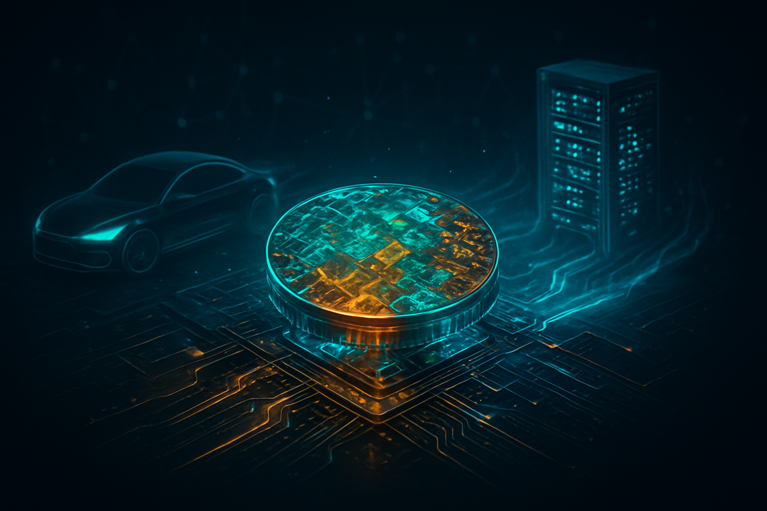
    On December 11, 2025, OpenAI shattered the growing industry narrative of a "plateau" in large language models with the surprise release of the GPT-5.2 series, internally codenamed "Garlic." This launch represents the most significant architectural pivot in the company's history, moving away from a single monolithic model toward a tiered ecosystem designed specifically for the high-stakes world of professional knowledge work. The release comes at a critical juncture for the San Francisco-based lab, arriving just weeks after internal reports of a "Code Red" crisis triggered by surging competition from rival labs.

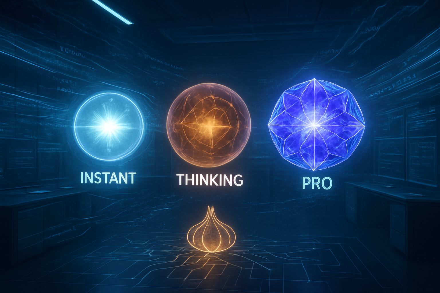
    The GPT-5.2 lineup is divided into three distinct iterations: Instant, Thinking, and Pro. While the Instant model focuses on the low-latency needs of daily interactions, it is the Thinking and Pro models that have sent shockwaves through the research community. By integrating advanced reasoning-effort settings that allow the model to "deliberate" before responding, OpenAI has achieved what many thought was years away: a perfect 100% score on the American Invitational Mathematics Examination (AIME) 2025 benchmark. This development signals a shift from AI as a conversational assistant to AI as a verifiable reasoning engine capable of tackling the world's most complex intellectual challenges.

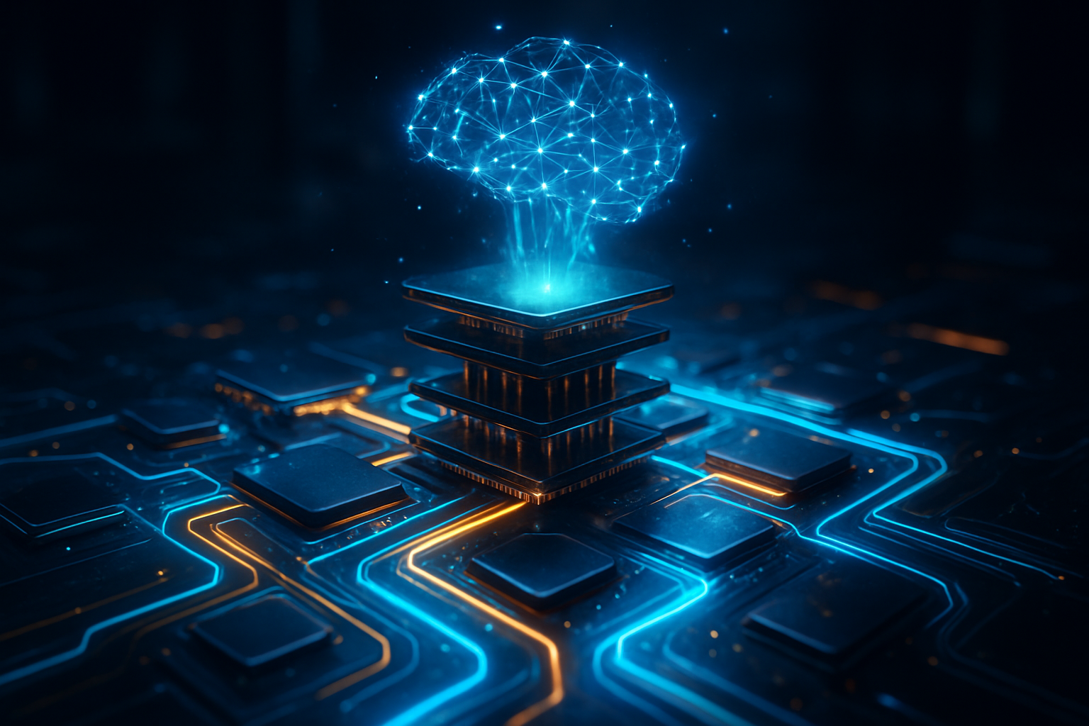
    Technical Breakthroughs: The Architecture of Deliberation

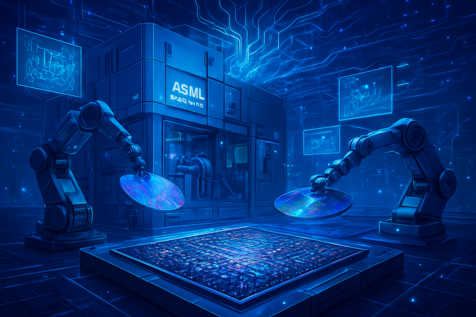
    The GPT-5.2 series marks a departure from the traditional "next-token prediction" paradigm, leaning heavily into reinforcement learning and "Chain-of-Thought" processing. The Thinking model is specifically engineered to handle "Artifacts"—complex, multi-layered digital objects such as dynamic financial models, interactive software prototypes, and 100-page legal briefs. Unlike its predecessors, GPT-5.2 Thinking can pause its output for several minutes to verify its internal logic, effectively debugging its own reasoning before the user ever sees a result. This "system 2" thinking approach has allowed the model to achieve a 55.6% success rate on the SWE-bench Pro, a benchmark for real-world software engineering that had previously stymied even the most advanced coding assistants.

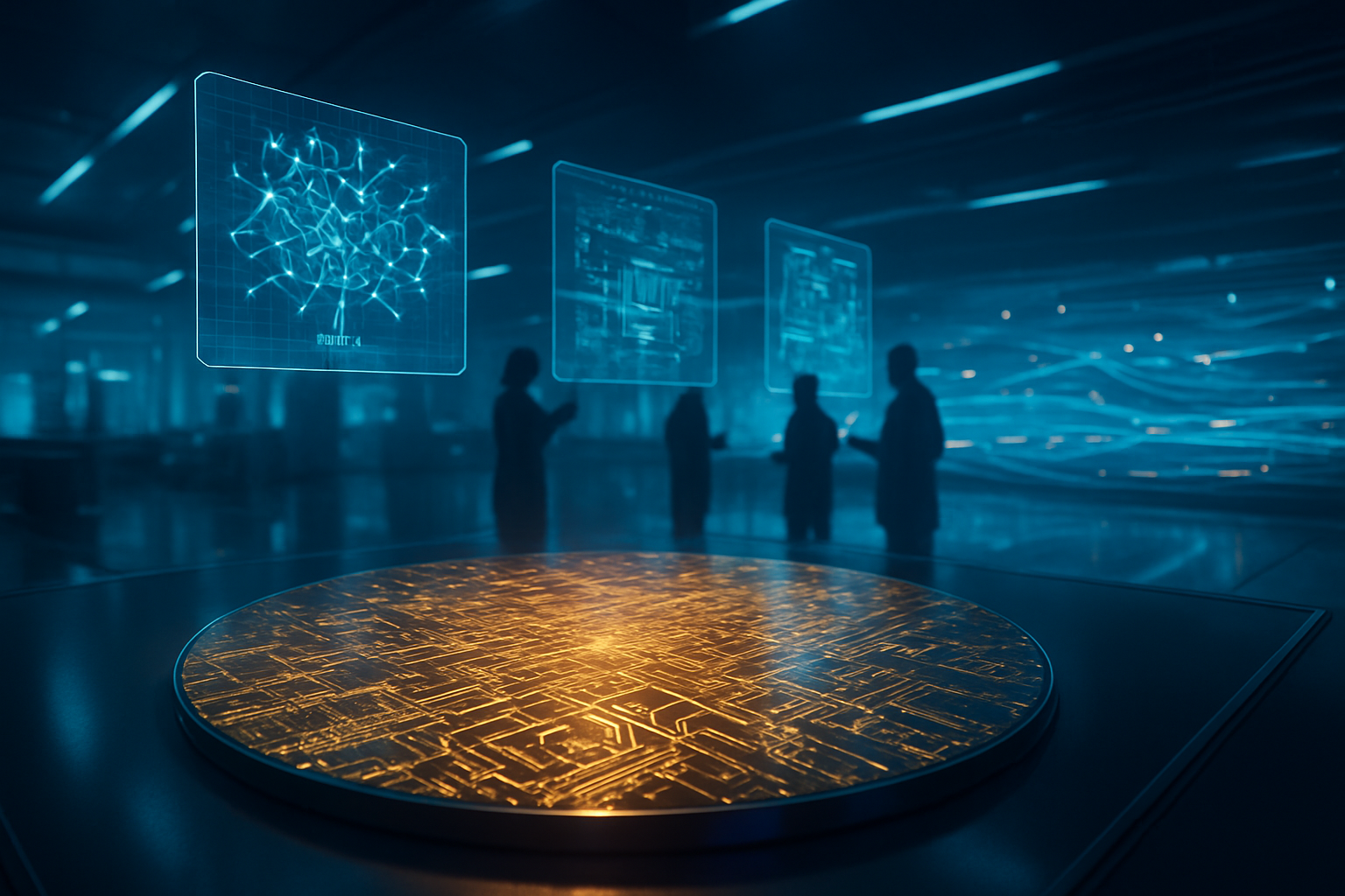
    For those requiring the absolute ceiling of machine intelligence, the GPT-5.2 Pro model offers a "research-grade" experience. Available via a new $200-per-month subscription tier, the Pro version can engage in reasoning tasks for over an hour, processing vast amounts of data to solve high-stakes problems where the margin for error is zero. In technical evaluations, the Pro model reached a historic 54.2% on the ARC-AGI-2 benchmark, crossing the 50% threshold for the first time in history and moving the industry significantly closer to the elusive goal of Artificial General Intelligence (AGI).

    This technical leap is further supported by a massive 400,000-token context window, allowing professional users to upload entire codebases or multi-year financial histories for analysis. Initial reactions from the AI research community have been a mix of awe and scrutiny. While many praise the unprecedented reasoning capabilities, some experts have noted that the model's tone has become significantly more formal and "colder" than the GPT-5.1 release, a deliberate choice by OpenAI to prioritize professional utility over social charm.

    The 'Code Red' Response: A Shifting Competitive Landscape

    The launch of "Garlic" was not merely a scheduled update but a strategic counter-strike. In late 2024 and early 2025, OpenAI faced an existential threat as Alphabet Inc. (NASDAQ: GOOGL) released Gemini 3 Pro and Anthropic (Private) debuted Claude Opus 4.5. Both models had begun to outperform GPT-5.1 in key areas of creative writing and coding, leading to a reported dip in ChatGPT's market share. In response, OpenAI CEO Sam Altman reportedly declared a "Code Red," pausing non-essential projects—including a personal assistant codenamed "Pulse"—to focus the company's entire engineering might on GPT-5.2.

    The strategic importance of this release was underscored by the simultaneous announcement of a $1 billion equity investment from The Walt Disney Company (NYSE: DIS). This landmark partnership positions Disney as a primary customer, utilizing GPT-5.2 to orchestrate complex creative workflows and becoming the first major content partner for Sora, OpenAI's video generation tool. This move provides OpenAI with a massive influx of capital and a prestigious enterprise sandbox, while giving Disney a significant technological lead in the entertainment industry.

    Other major tech players are already pivoting to integrate the new models. Shopify Inc. (NYSE: SHOP) and Zoom Video Communications, Inc. (NASDAQ: ZM) were announced as early enterprise testers, reporting that the agentic reasoning of GPT-5.2 allows for the automation of multi-step projects that previously required human oversight. For Microsoft Corp. (NASDAQ: MSFT), OpenAI’s primary partner, the success of GPT-5.2 reinforces the value of their multi-billion dollar investment, as these capabilities are expected to be integrated into the next generation of Copilot Pro tools.

    Redefining Knowledge Work and the Broader AI Landscape

    The most profound impact of GPT-5.2 may be its focus on the "professional knowledge worker." OpenAI introduced a new evaluation metric alongside the launch called GDPval, which measures AI performance across 44 occupations that contribute significantly to the global economy. GPT-5.2 achieved a staggering 70.9% win rate against human experts in these fields, compared to just 38.8% for the original GPT-5. This suggests that the era of AI as a simple "copilot" is evolving into an era of AI as an autonomous "agent" capable of executing end-to-end projects with minimal intervention.

    However, this leap in capability brings a new set of concerns. The cost of the Pro tier and the increased API pricing ($1.75 per 1 million input tokens) have raised questions about a growing "intelligence divide," where only the largest corporations and wealthiest individuals can afford the most capable reasoning engines. Furthermore, the model's ability to solve complex mathematical and engineering problems with 100% accuracy raises significant questions about the future of STEM education and the long-term value of human-led technical expertise.

    Compared to previous milestones like the launch of GPT-4 in 2023, the GPT-5.2 release feels less like a magic trick and more like a professional tool. It marks the transition of LLMs from being "good at everything" to being "expert at the difficult." The industry is now watching closely to see if the "Garlic" offensive will be enough to maintain OpenAI's lead as Google and Anthropic prepare their own responses for the 2026 cycle.

    The Road Ahead: Agentic Workflows and the AGI Horizon

    Looking forward, the success of the GPT-5.2 series sets the stage for a 2026 dominated by "agentic workflows." Experts predict that the next 12 months will see a surge in specialized AI agents that use the Thinking and Pro models as their "brains" to navigate the real world—managing supply chains, conducting scientific research, and perhaps even drafting legislation. The ability of GPT-5.2 to use tools independently and verify its own work is the foundational layer for these autonomous systems.

    Challenges remain, however, particularly in the realm of energy consumption and the "hallucination of logic." While GPT-5.2 has largely solved fact-based hallucinations, researchers warn that "reasoning hallucinations"—where a model follows a flawed but internally consistent logic path—could still occur in highly novel scenarios. Addressing these edge cases will be the primary focus of the rumored GPT-6 development, which is expected to begin in earnest now that the "Code Red" has subsided.

    Conclusion: A New Benchmark for Intelligence

    The launch of GPT-5.2 "Garlic" on December 11, 2025, will likely be remembered as the moment OpenAI successfully pivoted from a consumer-facing AI company to an enterprise-grade reasoning powerhouse. By delivering a model that can solve AIME-level math with perfect accuracy and provide deep, deliberative reasoning, they have raised the bar for what is expected of artificial intelligence. The introduction of the Instant, Thinking, and Pro tiers provides a clear roadmap for how AI will be consumed in the future: as a scalable resource tailored to the complexity of the task at hand.

    As we move into 2026, the tech industry will be defined by how well companies can integrate these "reasoning engines" into their daily operations. With the backing of giants like Disney and Microsoft, and a clear lead in the reasoning benchmarks, OpenAI has once again claimed the center of the AI stage. Whether this lead is sustainable in the face of rapid innovation from Google and Anthropic remains to be seen, but for now, the "Garlic" offensive has successfully changed the conversation from "Can AI think?" to "How much are you willing to pay for it to think for you?"


    This content is intended for informational purposes only and represents analysis of current AI developments.

    TokenRing AI delivers enterprise-grade solutions for multi-agent AI workflow orchestration, AI-powered development tools, and seamless remote collaboration platforms.
    For more information, visit https://www.tokenring.ai/.

  • The Green Silicon Revolution: How AI-Driven Mega-Fabs are Achieving 90% Water Circularity in the Race for Net Zero

    The Green Silicon Revolution: How AI-Driven Mega-Fabs are Achieving 90% Water Circularity in the Race for Net Zero

    As the global demand for high-performance artificial intelligence reaches a fever pitch in late 2025, the semiconductor industry is undergoing a radical transformation. Long criticized for its massive environmental footprint, the sector has pivoted toward "Sustainable Fabrication," a movement that has moved from corporate social responsibility reports to the very core of chip-making engineering. Today, the world’s leading "Mega-Fabs" are no longer just cathedrals of computation; they are marvels of resource efficiency, successfully decoupling the exponential growth of AI from the depletion of local ecosystems.

    The immediate significance of this shift cannot be overstated. With the deployment of the next generation of 2nm and 1.8A (18 Angstrom) nodes, water and energy requirements have historically threatened to outpace local infrastructure. However, a breakthrough in circular water systems—now capable of recycling up to 90% of the ultrapure water (UPW) used in manufacturing—has provided a lifeline. This transition to "Water Positive" and "Net Zero" status is not merely an environmental win; it has become a strategic necessity for securing government subsidies and maintaining a "license to operate" in drought-prone regions like Arizona, Taiwan, and South Korea.

    Engineering the Closed-Loop: The 90% Water Recovery Milestone

    The technical cornerstone of the 2025 sustainability push is the widespread implementation of advanced circular water systems. Modern semiconductor manufacturing requires billions of gallons of ultrapure water to rinse silicon wafers between hundreds of chemical processing steps. Historically, much of this water was treated and discharged. In 2025, however, Mega-Fabs operated by industry leaders have integrated Counterflow Reverse Osmosis (CFRO) and sophisticated drain segregation. Unlike previous generations of water treatment, CFRO utilizes specialized membranes—such as those developed by Toray—to remove trace ions and organic contaminants at parts-per-quadrillion levels, allowing "grey water" to be polished back into UPW for immediate reuse.

    This technical achievement is managed by a new layer of "Industrial AI Agents." These AI systems, integrated into the fab’s infrastructure, monitor over 20 different segregated chemical waste streams in real-time. By using predictive algorithms, these agents can adjust filtration pressures and chemical dosing dynamically, preventing the microscopic contamination that previously made 90% recycling rates a pipe dream. Initial reactions from the research community, including experts at the SMART USA Institute, suggest that these AI-managed systems have improved overall process yield by 40%, as they catch minute fluctuations in water quality before they can affect wafer integrity.

    The Competitive Edge: Sustainability as a Market Differentiator

    The push for green fabrication has created a new competitive landscape for the industry's giants. Intel (NASDAQ: INTC) has emerged as a frontrunner, announcing in December 2025 that its Fab 52 in Arizona has achieved "Net Positive Water" status—restoring more water to the local community than it consumes. This achievement, bolstered by their "WATR" (Water Conservation and Treatment) facilities, has positioned Intel as the preferred partner for government-backed projects under the U.S. CHIPS Act, which now mandates strict environmental benchmarks for funding.

    Similarly, Samsung (KRX: 005930) has leveraged its "Green GAA" (Gate-All-Around) architecture to secure high-profile 2nm orders from Tesla (NASDAQ: TSLA), Google (NASDAQ: GOOGL), and AMD (NASDAQ: AMD). These tech giants are increasingly under pressure to report "cradle-to-gate" carbon footprints, and Samsung’s Taylor, Texas fab—which utilizes a massive digital twin powered by Nvidia (NASDAQ: NVDA) GPUs to optimize energy loads—offers a measurable marketing advantage. TSMC (NYSE: TSM) has countered by accelerating its U.S. 2nm timeline, citing the successful validation of its on-site closed-loop water systems in Phoenix as a key reason for the move. For these companies, sustainability is no longer a cost center; it is a strategic asset that secures tier-one clients.

    The Wider Significance: Solving the Green Paradox of AI

    The broader significance of sustainable fabrication lies in its resolution of the "Green Paradox." While AI is a critical tool for solving climate change—optimizing power grids and discovering new battery chemistries—the hardware required to run these models has traditionally been an environmental liability. By 2025, the industry has demonstrated that the "virtuous cycle of silicon" can be self-sustaining. The use of AI to optimize the very factories that produce AI chips represents a major milestone in industrial evolution, mirroring the transition from the steam age to the electrical age.

    However, this transition has not been without concerns. Some environmental advocates argue that "Water Positive" status can be achieved through creative accounting, such as funding off-site conservation projects rather than reducing on-site consumption. To address this, the European Union has made the Digital Product Passport (DPP) mandatory as of 2025. This regulation requires a transparent, blockchain-verified account of every chip’s water and carbon footprint. This level of transparency is unprecedented and has set a global standard that effectively forces all manufacturers, including those in emerging markets, to adopt circular practices if they wish to access the lucrative European market.

    The Path to Total Water Independence

    Looking ahead, the next frontier for sustainable fabrication is the "Zero-Liquid Discharge" (ZLD) fab. While 90% circularity is the current gold standard, experts predict that by 2030, Mega-Fabs will reach 98% or higher, effectively operating as closed ecosystems that only require water to replace what is lost to evaporation. Near-term developments are expected to focus on "Atmospheric Water Generation" (AWG) at scale, where fabs could potentially pull their remaining water needs directly from the air using waste heat from their own cooling towers.

    Challenges remain, particularly regarding the energy intensity of these high-tech recycling systems. While water circularity is improving, the power required to run reverse osmosis and AI-driven monitoring systems adds to the fab's total energy load. The industry is now turning its attention to "on-site fusion" and advanced modular reactors (SMRs) to provide the carbon-free baseload power needed to keep these circular systems running 24/7. Experts predict that the next three years will see a flurry of partnerships between semiconductor firms and clean-energy startups to solve this final piece of the Net Zero puzzle.

    A New Standard for the Silicon Age

    As 2025 draws to a close, the semiconductor industry has successfully proven that high-tech manufacturing does not have to come at the expense of the planet's most precious resources. The achievement of 90% water recycling in Mega-Fabs is more than a technical win; it is a foundational shift in how we approach industrial growth in an era of climate volatility. The integration of AI as both a product and a tool for sustainability has created a blueprint that other heavy industries, from steel to chemicals, are now beginning to follow.

    The key takeaway from this year’s developments is that the "Green Silicon" era is officially here. The significance of this transition will likely be remembered as a turning point in AI history—the moment when the digital world finally learned to live in harmony with the physical one. In the coming months, watch for the first "DPP-certified" consumer devices to hit the shelves, as the environmental cost of a chip becomes as important to consumers as its clock speed.


    This content is intended for informational purposes only and represents analysis of current AI developments.

    TokenRing AI delivers enterprise-grade solutions for multi-agent AI workflow orchestration, AI-powered development tools, and seamless remote collaboration platforms.
    For more information, visit https://www.tokenring.ai/.

  • The Silent Revolution: How SiC and GaN are Powering the AI Infrastructure and EV Explosion

    The Silent Revolution: How SiC and GaN are Powering the AI Infrastructure and EV Explosion

    As of December 24, 2025, the semiconductor industry has reached a historic inflection point. The "Energy Wall"—a term coined by researchers to describe the physical limits of traditional silicon in high-power applications—has finally been breached. In its place, Wide-Bandgap (WBG) semiconductors, specifically Silicon Carbide (SiC) and Gallium Nitride (GaN), have emerged as the foundational pillars of the modern digital and automotive economy. These materials are no longer niche technologies for specialized hardware; they are now the essential components enabling the massive power demands of generative AI data centers and the 800-volt charging speeds of the latest electric vehicles (EVs).

    The significance of this transition cannot be overstated. With next-generation AI accelerators now drawing upwards of 2 kilowatts per package, the efficiency losses associated with legacy silicon-based power systems have become unsustainable. By leveraging the superior physical properties of SiC and GaN, engineers have managed to shrink power supply units by 50% while simultaneously slashing energy waste. This shift is effectively decoupling the growth of AI compute from the exponential rise in energy consumption, providing a critical lifeline for a power-hungry industry.

    Breaking the Silicon Ceiling: The Rise of 200mm and 300mm WBG

    The technical superiority of WBG materials lies in their "bandgap"—the energy required for electrons to move from the valence band to the conduction band. Traditional silicon has a bandgap of approximately 1.1 electron volts (eV), whereas SiC and GaN boast bandgaps of 3.2 eV and 3.4 eV, respectively. This allows these materials to operate at much higher voltages, temperatures, and frequencies without breaking down. In late 2025, the industry has successfully transitioned to 200mm (8-inch) SiC wafers, a move led by STMicroelectronics (NYSE: STM) at its Catania "Silicon Carbide Campus." This transition has increased chip yield per wafer by over 50%, finally bringing the cost of SiC closer to that of high-end silicon.

    Furthermore, 2025 has seen the commercial debut of Vertical GaN (vGaN), a breakthrough spearheaded by onsemi (NASDAQ: ON). Unlike traditional lateral GaN, which conducts current across the surface of the chip, vGaN conducts current through the substrate. This allows GaN to compete directly with SiC in the 1200V range, making it suitable for the heavy-duty traction inverters found in electric trucks and industrial machinery. Meanwhile, Infineon Technologies (OTC: IFNNY) has begun sampling the world’s first 300mm GaN-on-Silicon wafers, a feat that promises to revolutionize the economics of power electronics by leveraging existing high-volume silicon manufacturing lines.

    These advancements differ from previous technologies by offering a "triple threat" of benefits: higher switching frequencies, lower on-resistance, and superior thermal conductivity. In practical terms, this means that power converters can use smaller capacitors and inductors, leading to more compact and lightweight designs. Industry experts have lauded these developments as the most significant change in power electronics since the invention of the MOSFET in the 1960s, noting that the "Silicon-only" era of power management is effectively over.

    Market Dominance and the AI Power Supply Gold Rush

    The shift toward WBG materials has triggered a massive realignment among semiconductor giants. STMicroelectronics (NYSE: STM) currently holds a commanding 29% share of the SiC market, largely due to its long-standing partnership with major EV manufacturers and its early investment in 200mm production. However, onsemi (NASDAQ: ON) has rapidly closed the gap, securing multi-billion dollar long-term supply agreements with automotive OEMs and emerging as the leader in the newly formed vGaN segment.

    The AI data center market has become the new primary battleground for these companies. As hyperscalers like Amazon and Google deploy 12kW Power Supply Units (PSUs) to support the latest AI clusters, the demand for GaN has skyrocketed. These PSUs, which utilize SiC for high-voltage AC-DC conversion and GaN for high-frequency DC-DC switching, achieve 98% efficiency. This is a critical metric for data center operators, as every 1% increase in efficiency can save millions of dollars in electricity and cooling costs annually.

    The competitive landscape has also seen dramatic shifts for legacy players. Wolfspeed (NYSE: WOLF), once the pure-play leader in SiC, emerged from a successful Chapter 11 restructuring in September 2025. With its Mohawk Valley Fab finally reaching 30% utilization, the company is stabilizing its supply chain and refocusing on high-purity SiC substrates, where it still holds a 33% global market share. This restructuring has allowed Wolfspeed to remain a vital supplier to other chipmakers while shedding the debt that hampered its growth during the 2024 downturn.

    Societal Impact: Efficiency as the New Sustainability

    The broader significance of the WBG revolution extends far beyond corporate balance sheets; it is a critical component of global sustainability efforts. In the EV sector, the adoption of 800V architectures enabled by SiC has virtually eliminated "range anxiety" for the average consumer. By allowing for 15-minute "flash charging" and increasing vehicle range by 7-10% without increasing battery size, WBG materials are making EVs more practical and affordable for the mass market.

    In the realm of AI, WBG semiconductors are solving the "PUE Crisis" (Power Usage Effectiveness). By reducing the heat generated during power conversion, these materials have lowered the energy demand of data center cooling systems by an estimated 40%. This allows AI companies to pack more compute density into existing facilities, delaying the need for costly new grid connections and reducing the environmental footprint of large language model training.

    However, the rapid transition has not been without concerns. The concentration of SiC substrate production remains a geopolitical flashpoint, with Chinese players like SICC and Tankeblue aggressively gaining market share and undercutting Western prices. This has led to increased calls for "local-for-local" supply chains to ensure that the critical infrastructure of the AI era is not vulnerable to trade disruptions.

    The Horizon: Ultra-Wide Bandgap and AI-Optimized Power

    Looking ahead to 2026 and beyond, the industry is already eyeing the next frontier: Ultra-Wide Bandgap (UWBG) materials. Research into Gallium Oxide and Diamond-based semiconductors is accelerating, with the goal of creating chips that can handle even higher voltages and temperatures than SiC. These materials could eventually power the next generation of orbital satellites and deep-sea exploration equipment, where environmental conditions are too extreme for current technology.

    Another burgeoning field is "Cognitive Power Electronics." Tesla recently revealed a system that uses real-time AI to adjust SiC switching frequencies based on driving conditions and battery state-of-health. This software-defined approach to power management allows for a 75% reduction in SiC content while maintaining the same level of performance, potentially lowering the cost of entry-level EVs. Experts predict that this marriage of AI and WBG hardware will become the standard for all high-performance energy systems by the end of the decade.

    A New Era for Energy and Intelligence

    The transition to Silicon Carbide and Gallium Nitride represents a fundamental shift in how humanity manages energy. By moving past the physical limitations of silicon, the semiconductor industry has provided the necessary infrastructure to support the dual revolutions of artificial intelligence and electrified transportation. The developments of 2025 have proven that efficiency is not just a secondary goal, but a primary enabler of technological progress.

    As we move into 2026, the key metrics to watch will be the continued scaling of 300mm GaN production and the integration of AI-driven material discovery to further enhance chip reliability. The "Silent Revolution" of WBG semiconductors may not always capture the headlines like the latest AI model, but it is the indispensable engine driving the future of innovation.


    This content is intended for informational purposes only and represents analysis of current AI developments.

    TokenRing AI delivers enterprise-grade solutions for multi-agent AI workflow orchestration, AI-powered development tools, and seamless remote collaboration platforms.
    For more information, visit https://www.tokenring.ai/.

  • The Chiplet Revolution: How Advanced Packaging and UCIe are Redefining AI Hardware in 2025

    The Chiplet Revolution: How Advanced Packaging and UCIe are Redefining AI Hardware in 2025

    The semiconductor industry has reached a historic inflection point as the "Chiplet Revolution" transitions from a visionary concept into the bedrock of global compute. As of late 2025, the era of the massive, single-piece "monolithic" processor is effectively over for high-performance applications. In its place, a sophisticated ecosystem of modular silicon components—known as chiplets—is being "stitched" together using advanced packaging techniques that were once considered experimental. This shift is not merely a manufacturing preference; it is a survival strategy for a world where the demand for AI compute is doubling every few months, far outstripping the slow gains of traditional transistor scaling.

    The immediate significance of this revolution lies in the democratization of high-end silicon. With the recent ratification of the Universal Chiplet Interconnect Express (UCIe) 3.0 standard in August 2025, the industry has finally established a "lingua franca" that allows chips from different manufacturers to communicate as if they were on the same piece of silicon. This interoperability is breaking the proprietary stranglehold held by the largest chipmakers, enabling a new wave of "mix-and-match" processors where a company might combine an Intel Corporation (NASDAQ:INTC) compute tile with an NVIDIA (NASDAQ:NVDA) AI accelerator and Samsung Electronics (OTC:SSNLF) memory, all within a single, high-performance package.

    The Architecture of Interconnects: UCIe 3.0 and the 3D Frontier

    Technically, the "stitching" of these dies relies on the UCIe standard, which has seen rapid iteration over the last 18 months. The current benchmark, UCIe 3.0, offers staggering data rates of 64 GT/s per lane, doubling the bandwidth of the previous generation while maintaining ultra-low latency. This is achieved through "UCIe-3D" optimizations, which are specifically designed for hybrid bonding—a process that allows dies to be stacked vertically with copper-to-copper connections. These connections are now reaching bump pitches as small as 1 micron, effectively turning a stack of chips into a singular, three-dimensional block of logic and memory.

    This approach differs fundamentally from previous "System-on-Chip" (SoC) designs. In the past, if one part of a large chip was defective, the entire expensive component had to be discarded. Today, companies like Advanced Micro Devices (NASDAQ:AMD) and NVIDIA use "binning" at the chiplet level, significantly increasing yields and lowering costs. For instance, NVIDIA’s Blackwell architecture (B200) utilizes a dual-die "superchip" design connected via a 10 TB/s link, a feat of engineering that would have been physically impossible on a single monolithic die due to the "reticle limit"—the maximum size a chip can be printed by current lithography machines.

    However, the transition to 3D stacking has introduced a new set of manufacturing hurdles. Thermal management has become the industry’s "white whale," as stacking high-power logic dies creates concentrated hot spots that traditional air cooling cannot dissipate. In late 2025, liquid cooling and even "in-package" microfluidic channels have moved from research labs to data center floors to prevent these 3D stacks from melting. Furthermore, the industry is grappling with the yield rates of 16-layer HBM4 (High Bandwidth Memory), which currently hover around 60%, creating a significant cost barrier for mass-market adoption.

    Strategic Realignment: The Packaging Arms Race

    The shift toward chiplets has fundamentally altered the competitive landscape for tech giants and startups alike. Taiwan Semiconductor Manufacturing Company (NYSE:TSM), or TSMC, has seen its CoWoS (Chip-on-Wafer-on-Substrate) packaging technology become the most sought-after commodity in the world. With capacity reaching 80,000 wafers per month by December 2025, TSMC remains the gatekeeper of AI progress. This dominance has forced competitors and customers to seek alternatives, leading to the rise of secondary packaging providers like Powertech Technology Inc. (TWSE:6239) and the acceleration of Intel’s "IDM 2.0" strategy, which positions its Foveros packaging as a direct rival to TSMC.

    For AI labs and hyperscalers like Amazon (NASDAQ:AMZN) and Alphabet (NASDAQ:GOOGL), the chiplet revolution offers a path to sovereignty. By using the UCIe standard, these companies can design their own custom "accelerator" chiplets and pair them with industry-standard I/O and memory dies. This reduces their dependence on off-the-shelf parts and allows for hardware that is hyper-optimized for specific AI workloads, such as large language model (LLM) inference or protein folding simulations. The strategic advantage has shifted from who has the best lithography to who has the most efficient packaging and interconnect ecosystem.

    The disruption is also being felt in the consumer sector. Intel’s Arrow Lake and Lunar Lake processors represent the first mainstream desktop and mobile chips to fully embrace 3D "tiled" architectures. By outsourcing specific tiles to TSMC while performing the final assembly in-house, Intel has managed to stay competitive in power efficiency, a move that would have been unthinkable five years ago. This "fab-agnostic" approach is becoming the new standard, as even the most vertically integrated companies realize they cannot lead in every single sub-process of semiconductor manufacturing.

    Beyond Moore’s Law: The Wider Significance of Modular Silicon

    The chiplet revolution is the definitive answer to the slowing of Moore’s Law. As the physical limits of transistor shrinking are reached, the industry has pivoted to "More than Moore"—a philosophy that emphasizes system-level integration over raw transistor density. This trend fits into a broader AI landscape where the size of models is growing exponentially, requiring a corresponding leap in memory bandwidth and interconnect speed. Without the "stitching" capabilities of UCIe and advanced packaging, the hardware would have hit a performance ceiling in 2023, potentially stalling the current AI boom.

    However, this transition brings new concerns regarding supply chain security and geopolitical stability. Because a single advanced package might contain components from three different countries and four different companies, the "provenance" of silicon has become a major headache for defense and government sectors. The complexity of testing these multi-die systems also introduces potential vulnerabilities; a single compromised chiplet could theoretically act as a "Trojan horse" within a larger system. As a result, the UCIe 3.0 standard has introduced a standardized "UDA" (UCIe DFx Architecture) for better testability and security auditing.

    Compared to previous milestones, such as the introduction of FinFET transistors or EUV lithography, the chiplet revolution is more of a structural shift than a purely scientific one. It represents the "industrialization" of silicon, moving away from the artisan-like creation of single-block chips toward a modular, assembly-line approach. This maturity is necessary for the next phase of the AI era, where compute must become as ubiquitous and scalable as electricity.

    The Horizon: Glass Substrates and Optical Interconnects

    Looking ahead to 2026 and beyond, the next major breakthrough is already in pilot production: glass substrates. Led by Intel and partners like SKC Co., Ltd. (KRX:011790) through its subsidiary Absolics, glass is set to replace the organic (plastic) substrates that have been the industry standard for decades. Glass offers superior flatness and thermal stability, allowing for even denser interconnects and faster signal speeds. Experts predict that glass substrates will be the key to enabling the first "trillion-transistor" packages by 2027.

    Another area of intense development is the integration of silicon photonics directly into the chiplet stack. As copper wires struggle to carry data across 100mm distances without significant heat and signal loss, light-based interconnects are becoming a necessity. Companies are currently working on "optical I/O" chiplets that could allow different parts of a data center to communicate at the same speeds as components on the same board. This would effectively turn an entire server rack into a single, giant, distributed computer.

    A New Era of Computing

    The "Chiplet Revolution" of 2025 has fundamentally rewritten the rules of the semiconductor industry. By moving from a monolithic to a modular philosophy, the industry has found a way to sustain the breakneck pace of AI development despite the mounting physical challenges of silicon manufacturing. The UCIe standard has acted as the crucial glue, allowing a diverse ecosystem of manufacturers to collaborate on a single piece of hardware, while advanced packaging has become the new frontier of competitive advantage.

    As we look toward 2026, the focus will remain on scaling these technologies to meet the insatiable demands of the "Blackwell-class" and "Rubin-class" AI architectures. The transition to glass substrates and the maturation of 3D stacking yields will be the primary metrics of success. For now, the "Silicon Stitch" has successfully extended the life of Moore's Law, ensuring that the AI revolution has the hardware it needs to continue its transformative journey.


    This content is intended for informational purposes only and represents analysis of current AI developments.

    TokenRing AI delivers enterprise-grade solutions for multi-agent AI workflow orchestration, AI-powered development tools, and seamless remote collaboration platforms.
    For more information, visit https://www.tokenring.ai/.

  • The Silicon Backbone: How the AI Revolution Triggered a $52 Billion Semiconductor Talent War

    The Silicon Backbone: How the AI Revolution Triggered a $52 Billion Semiconductor Talent War

    As the global race for artificial intelligence supremacy accelerates, the industry has hit a formidable and unexpected bottleneck: a critical shortage of the human experts required to build the hardware that powers AI. As of late 2025, the United States semiconductor industry is grappling with a staggering "talent war," characterized by more than 25,000 immediate job openings across the "Silicon Desert" of Arizona and the "Silicon Heartland" of Ohio. This labor crisis threatens to derail the ambitious domestic manufacturing goals set by the CHIPS and Science Act, as the demand for 2nm and below processing nodes outstrips the supply of qualified engineers and technicians.

    The immediate significance of this development cannot be overstated. While the federal government has committed billions to build physical fabrication plants (fabs), the lack of a specialized workforce has turned into a primary risk factor for project timelines. From entry-level fab technicians to PhD-level Extreme Ultraviolet (EUV) lithography experts, the industry is pivoting away from traditional recruitment models toward aggressive "skills academies" and unprecedented university partnerships. This shift marks a fundamental restructuring of how the tech industry prepares its workforce for the era of hardware-defined AI.

    From Degrees to Certifications: The Rise of Semiconductor Skills Academies

    The current talent gap is not merely a numbers problem; it is a specialized skills mismatch. Of the 25,000+ current openings, a significant portion is for mid-level technicians who do not necessarily require a four-year engineering degree but do need highly specific training in cleanroom protocols and vacuum systems. To address this, industry leaders like Intel (NASDAQ:INTC) have pioneered "Quick Start" programs. In Arizona, Intel partnered with Maricopa Community Colleges to offer a two-week intensive program that transitions workers from adjacent industries—such as automotive or aerospace—into entry-level semiconductor roles.

    Technically, these programs are a departure from the "ivory tower" approach to engineering. They utilize "digital twin" training environments—virtual replicas of multi-billion dollar fabs—allowing students to practice complex maintenance on EUV machines without risking damage to actual equipment. This technical shift is supported by the National Semiconductor Technology Center (NSTC) Workforce Center of Excellence, which received a $250 million investment in early 2025 to standardize these digital training modules nationwide.

    Initial reactions from the AI research community have been cautiously optimistic. Experts note that while these "skills academies" can solve the technician shortage, the "brain drain" at the higher end of the spectrum—specifically in advanced packaging and circuit design—remains acute. The complexity of 2nm chip architectures requires a level of physics and materials science expertise that cannot be fast-tracked in a two-week boot camp, leading to a fierce bidding war for graduate-level talent.

    Corporate Giants and the Strategic Hunt for Human Capital

    The talent war has created a new competitive landscape where a company’s valuation is increasingly tied to its ability to secure a workforce. Intel (NASDAQ:INTC) has been the most aggressive, committing $100 million to its Semiconductor Education and Research Program (SERP). By embedding itself in the curriculum of eight leading Ohio universities, including Ohio State, Intel is effectively "pre-ordering" the next generation of graduates to staff its $20 billion manufacturing hub in Licking County.

    TSMC (NYSE:TSM) has followed a similar playbook in Arizona. By partnering with Arizona State University (ASU) through the CareerCatalyst platform, TSMC is leveraging non-degree, skills-based education to fill its Phoenix-based fabs. This move is a strategic necessity; TSMC’s expansion into the U.S. has been historically hampered by cultural and technical differences in workforce management. By funding local training centers, TSMC is attempting to build a "homegrown" workforce that can operate its most advanced 3nm and 2nm lines.

    Meanwhile, Micron (NASDAQ:MU) has looked toward international cooperation to solve the domestic shortage. Through the UPWARDS Network, a $60 million initiative involving Tokyo Electron (OTC:TOELY) and several U.S. and Japanese universities, Micron is cultivating a global talent pool. This cross-border strategy provides a competitive advantage by allowing Micron to tap into the specialized lithography expertise of Japanese engineers while training U.S. students at Purdue University and Virginia Tech.

    National Security and the Broader AI Landscape

    The semiconductor talent war is more than just a corporate HR challenge; it is a matter of national security and a critical pillar of the global AI landscape. The 2024-2025 surge in AI-specific chips has made it clear that the "software-first" mentality of the last decade is no longer sufficient. Without a robust workforce to operate domestic fabs, the U.S. remains vulnerable to supply chain disruptions that could freeze AI development overnight.

    This situation echoes previous milestones in tech history, such as the 1960s space race, where the government and private sector had to fundamentally realign the education system to meet a national objective. However, the current crisis is complicated by the fact that the semiconductor industry is competing for the same pool of STEM talent as the high-paying software and finance sectors. There are growing concerns that the "talent war" could lead to a cannibalization of other critical tech industries if not managed through a broad expansion of the total talent pool.

    Furthermore, the focus on "skills academies" and rapid certification raises questions about long-term innovation. While these programs fill the immediate 25,000-job gap, some industry veterans worry that a shift away from deep, fundamental research in favor of vocational training could slow the breakthrough discoveries needed for post-silicon computing or room-temperature superconductors.

    The Future of Silicon Engineering: Automation and Digital Twins

    Looking ahead to 2026 and beyond, the industry is expected to turn toward AI itself to solve the human talent shortage. "AI for EDA" (Electronic Design Automation) is a burgeoning field where machine learning models assist in the layout and verification of complex circuits, potentially reducing the number of human engineers required for a single project. We are also likely to see the expansion of "lights-out" manufacturing—fully automated fabs that require fewer human technicians on the floor, though this will only increase the demand for high-level software engineers to maintain the automation systems.

    In the near term, the success of the CHIPS Act will be measured by the graduation rates of programs like Purdue’s Semiconductor Degrees Program (SDP) and the STARS (Summer Training, Awareness, and Readiness for Semiconductors) initiative. Experts predict that if these university-corporate partnerships can bridge 50% of the projected 67,000-worker shortfall by 2030, the U.S. will have successfully secured its position as a global semiconductor powerhouse.

    A Decisive Moment for the Hardware Revolution

    The 25,000-job opening gap in the semiconductor industry is a stark reminder that the AI revolution is built on a foundation of physical hardware and human labor. The transition from traditional academic pathways to agile "skills academies" and deep corporate-university integration represents one of the most significant shifts in technical education in decades. As Intel, TSMC, and Micron race to staff their new facilities, the winners of the talent war will likely be the winners of the AI era.

    Key takeaways from this development include the critical role of federal funding in workforce infrastructure, the rising importance of "digital twin" training technologies, and the strategic necessity of regional talent hubs. In the coming months, industry watchers should keep a close eye on the first wave of graduates from the Intel-Ohio and TSMC-ASU partnerships. Their ability to seamlessly integrate into high-stakes fab environments will determine whether the U.S. can truly bring the silicon backbone of AI back to its own shores.


    This content is intended for informational purposes only and represents analysis of current AI developments.

    TokenRing AI delivers enterprise-grade solutions for multi-agent AI workflow orchestration, AI-powered development tools, and seamless remote collaboration platforms.
    For more information, visit https://www.tokenring.ai/.

  • The Silicon Sovereignty: How the ‘AI PC’ Revolution of 2025 Ended the Cloud’s Monopoly on Intelligence

    The Silicon Sovereignty: How the ‘AI PC’ Revolution of 2025 Ended the Cloud’s Monopoly on Intelligence

    As we close out 2025, the technology landscape has undergone its most significant architectural shift since the transition from mainframes to personal computers. The "AI PC"—once dismissed as a marketing buzzword in early 2024—has become the undisputed industry standard. By moving generative AI processing from massive, energy-hungry data centers directly onto the silicon of laptops and smartphones, the industry has fundamentally rewritten the rules of privacy, latency, and digital agency.

    This shift toward local AI processing is driven by the maturation of dedicated Neural Processing Units (NPUs) and high-performance integrated graphics. Today, nearly 40% of all global PC shipments are classified as "AI-capable," meaning they possess the specialized hardware required to run Large Language Models (LLMs) and diffusion models without an internet connection. This "Silicon Sovereignty" marks the end of the cloud-first era, as users reclaim control over their data and their compute power.

    The Rise of the NPU: From 10 to 80 TOPS in Two Years

    In late 2025, the primary metric for computing power is no longer just clock speed or core count, but TOPS (Tera Operations Per Second). The industry has standardized a baseline of 45 to 50 NPU TOPS for any device carrying the "Copilot+" certification from Microsoft (NASDAQ: MSFT). This represents a staggering leap from the 10-15 TOPS seen in the first generation of AI-enabled chips. Leading the charge is Qualcomm (NASDAQ: QCOM) with its Snapdragon X2 Elite, which boasts a dedicated NPU capable of 80 TOPS. This allows for real-time, multi-modal AI interactions—such as live translation and screen-aware assistance—with negligible impact on the device's 22-hour battery life.

    Intel (NASDAQ: INTC) has responded with its Panther Lake architecture, built on the cutting-edge Intel 18A process, which emphasizes "Total Platform TOPS." By orchestrating the CPU, NPU, and the new Xe3 GPU in tandem, Intel-based machines can reach a combined 180 TOPS, providing enough headroom to run sophisticated "Agentic AI" that can navigate complex software interfaces on behalf of the user. Meanwhile, AMD (NASDAQ: AMD) has targeted the high-end creator market with its Ryzen AI Max 300 series. These chips feature massive integrated GPUs that allow enthusiasts to run 70-billion parameter models, like Llama 3, entirely on a laptop—a feat that required a server rack just 24 months ago.

    This technical evolution differs from previous approaches by solving the "memory wall." Modern AI PCs now utilize on-package memory and high-bandwidth unified architectures to ensure that the massive data sets required for AI inference don't bottleneck the processor. The result is a user experience where AI isn't a separate app you visit, but a seamless layer of the operating system that anticipates needs, summarizes local documents instantly, and generates content with zero round-trip latency to a remote server.

    A New Power Dynamic: Winners and Losers in the Local AI Era

    The move to local processing has created a seismic shift in market positioning. Silicon giants like Intel, AMD, and Qualcomm have seen a resurgence in relevance as the "PC upgrade cycle" finally accelerated after years of stagnation. However, the most dominant player remains NVIDIA (NASDAQ: NVDA). While NPUs handle background tasks, NVIDIA’s RTX 50-series GPUs, featuring the Blackwell architecture, offer upwards of 3,000 TOPS. By branding these as "Premium AI PCs," NVIDIA has captured the developer and researcher market, ensuring that anyone building the next generation of AI does so on their proprietary CUDA and TensorRT software stacks.

    Software giants are also pivoting. Microsoft and Apple (NASDAQ: AAPL) are no longer just selling operating systems; they are selling "Personal Intelligence." With the launch of the M5 chip and "Apple Intelligence Pro," Apple has integrated AI accelerators directly into every GPU core, allowing for a multimodal Siri that can perform cross-app actions securely. This poses a significant threat to pure-play AI startups that rely on cloud-based subscription models. If a user can run a high-quality LLM locally for free on their MacBook or Surface, the value proposition of paying $20 a month for a cloud-based chatbot begins to evaporate.

    Furthermore, this development disrupts the traditional cloud service providers. As more inference moves to the edge, the demand for massive cloud-AI clusters may shift toward training rather than daily execution. Companies like Adobe (NASDAQ: ADBE) have already adapted by moving their Firefly generative tools to run locally on NPU-equipped hardware, reducing their own server costs while providing users with faster, more private creative workflows.

    Privacy, Sovereignty, and the Death of the 'Dumb' OS

    The wider significance of the AI PC revolution lies in the concept of "Sovereign AI." In 2024, the primary concern for enterprise and individual users was data leakage—the fear that sensitive information sent to a cloud AI would be used to train future models. In 2025, that concern has been largely mitigated. Local AI processing means that a user’s "semantic index"—the total history of their files, emails, and screen activity—never leaves the device. This has enabled features like the matured version of Windows Recall, which acts as a perfect photographic memory for your digital life without compromising security.

    This transition mirrors the broader trend of decentralization in technology. Much like the PC liberated users from the constraints of time-sharing on mainframes, the AI PC is liberating users from the "intelligence-sharing" of the cloud. It represents a move toward an "Agentic OS," where the operating system is no longer a passive file manager but an active participant in the user's workflow. This shift has also sparked a renaissance in open-source AI; platforms like LM Studio and Ollama have become mainstream, allowing non-technical users to download and run specialized models tailored for medicine, law, or coding with a single click.

    However, this milestone is not without concerns. The "TOPS War" has led to increased power consumption in high-end laptops, and the environmental impact of manufacturing millions of new, AI-specialized chips is a subject of intense debate. Additionally, as AI becomes more integrated into the local OS, the potential for "local-side" malware that targets an individual's private AI model is a new frontier for cybersecurity experts.

    The Horizon: From Assistants to Autonomous Agents

    Looking ahead to 2026 and beyond, we expect the NPU baseline to cross the 100 TOPS threshold for even entry-level devices. This will usher in the era of truly autonomous agents—AI entities that don't just suggest text, but actually execute multi-step projects across different software environments. We will likely see the emergence of "Personal Foundation Models," AI systems that are fine-tuned on a user's specific voice, style, and professional knowledge base, residing entirely on their local hardware.

    The next challenge for the industry will be the "Memory Bottleneck." While NPU speeds are skyrocketing, the ability to feed these processors data quickly enough remains a hurdle. We expect to see more aggressive moves toward 3D-stacked memory and new interconnect standards designed specifically for AI-heavy workloads. Experts also predict that the distinction between a "smartphone" and a "PC" will continue to blur, as both devices will share the same high-TOPS silicon architectures, allowing a seamless AI experience that follows the user across all screens.

    Summary: A New Chapter in Computing History

    The emergence of the AI PC in 2025 marks a definitive turning point in the history of artificial intelligence. By successfully decentralizing intelligence, the industry has addressed the three biggest hurdles to AI adoption: cost, latency, and privacy. The transition from cloud-dependent chatbots to local, NPU-driven agents has transformed the personal computer from a tool we use into a partner that understands us.

    Key takeaways from this development include the standardization of the 50 TOPS NPU, the strategic pivot of silicon giants like Intel and Qualcomm toward edge AI, and the rise of the "Agentic OS." In the coming months, watch for the first wave of "AI-native" software applications that abandon the cloud entirely, as well as the ongoing battle between NVIDIA's high-performance discrete GPUs and the increasingly capable integrated NPUs from its competitors. The era of Silicon Sovereignty has arrived, and the cloud will never be the same.


    This content is intended for informational purposes only and represents analysis of current AI developments.

    TokenRing AI delivers enterprise-grade solutions for multi-agent AI workflow orchestration, AI-powered development tools, and seamless remote collaboration platforms.
    For more information, visit https://www.tokenring.ai/.

  • The Angstrom Era Arrives: How ASML’s $400 Million High-NA Tools Are Forging the Future of AI

    The Angstrom Era Arrives: How ASML’s $400 Million High-NA Tools Are Forging the Future of AI

    As of late 2025, the semiconductor industry has officially crossed the threshold into the "Angstrom Era," a pivotal transition that marks the end of the nanometer-scale naming convention and the beginning of atomic-scale precision. This shift is being driven by the deployment of High-Numerical Aperture (High-NA) Extreme Ultraviolet (EUV) lithography, a technological feat centered around ASML (NASDAQ: ASML) and its massive TWINSCAN EXE:5200B scanners. These machines, which now command a staggering price tag of nearly $400 million each, are the essential "printing presses" for the next generation of 1.8nm and 1.4nm chips that will power the increasingly demanding AI models of the late 2020s.

    The immediate significance of this development cannot be overstated. While the previous generation of EUV tools allowed the industry to reach the 3nm threshold, the move to 1.8nm (Intel 18A) and beyond requires a level of resolution that standard EUV simply cannot provide without extreme complexity. By increasing the numerical aperture from 0.33 to 0.55, ASML has enabled chipmakers to print features as small as 8nm in a single pass. This breakthrough is the cornerstone of Intel’s (NASDAQ: INTC) aggressive strategy to reclaim the process leadership crown, signaling a massive shift in the competitive landscape between the United States, Taiwan, and South Korea.

    The Technical Leap: From 0.33 to 0.55 NA

    The transition to High-NA EUV represents the most significant change in lithography since the introduction of EUV itself. At the heart of the ASML TWINSCAN EXE:5200B is a completely redesigned optical system. Standard EUV tools use a 0.33 NA lens, which, while revolutionary, hit a physical limit when trying to print features for nodes below 2nm. To achieve the necessary density, manufacturers were forced to use "multi-patterning"—essentially printing a single layer multiple times to create finer lines—which increased production time, lowered yields, and spiked costs. High-NA EUV solves this by using a 0.55 NA system, allowing for a nearly threefold increase in transistor density and reducing the number of critical mask steps from over 40 to single digits.

    However, this leap comes with immense technical challenges. High-NA scanners utilize an "anamorphic" lens design, which means they magnify the image differently in the horizontal and vertical directions. This results in a "half-field" exposure, where the scanner only prints half the area of a standard mask at once. To overcome this, the industry has had to master "mask stitching," a process where two exposures are perfectly aligned to create a single large chip. This required a massive overhaul of Electronic Design Automation (EDA) tools from companies like Synopsys (NASDAQ: SNPS) and Cadence (NASDAQ: CDNS), which now use AI-driven algorithms to ensure layouts are "stitching-aware."

    The technical specifications of the EXE:5200B are equally daunting. The machine weighs over 150 tons and requires two Boeing 747s to transport. Despite its size, it maintains a throughput of 175 to 200 wafers per hour, a critical metric for high-volume manufacturing (HVM). Furthermore, because the 8nm resolution requires incredibly thin photoresists, the industry has shifted toward Metal Oxide Resists (MOR) and dry-resist technology, pioneered by companies like Applied Materials (NASDAQ: AMAT), to prevent the collapse of the tiny transistor structures during the etching process.

    A Divided Industry: Strategic Bets on the Angstrom Era

    The adoption of High-NA EUV has created a fascinating strategic divide among the world's top chipmakers. Intel has taken the most aggressive stance, positioning itself as the "first-mover" in the High-NA space. By late 2025, Intel has successfully integrated High-NA tools into its 18A (1.8nm) production line to optimize critical layers and is using the technology as the foundation for its upcoming 14A (1.4nm) node. This "all-in" bet is designed to leapfrog TSMC (NYSE: TSM) and prove that Intel's RibbonFET (Gate-All-Around) and PowerVia (backside power delivery) architectures are superior when paired with the world's most advanced lithography.

    In contrast, TSMC has adopted a more cautious, "prudent" path. The Taiwanese giant has opted to skip High-NA for its A16 (1.6nm) and A14 (1.4nm) nodes, instead relying on "hyper-multi-patterning" with standard 0.33 NA EUV tools. TSMC’s leadership argues that the cost and complexity of High-NA do not yet justify the benefits for their current customer base, which includes Apple and Nvidia. TSMC expects to wait until the A10 (1nm) node, likely around 2028, to fully embrace High-NA. This creates a high-stakes experiment: can Intel’s technological edge overcome TSMC’s massive scale and proven manufacturing efficiency?

    Samsung Electronics (KRX: 005930) has taken a middle-ground approach. While it took delivery of an R&D High-NA tool (the EXE:5000) in early 2025, it is focusing its commercial High-NA efforts on its SF1.4 (1.4nm) node, slated for 2027. This phased adoption allows Samsung to learn from the early challenges faced by Intel while ensuring it doesn't fall as far behind as TSMC might if Intel’s bet pays off. For AI startups and fabless giants, this split means choosing between the "bleeding edge" performance of Intel’s High-NA nodes or the "mature reliability" of TSMC’s standard EUV nodes.

    The Broader AI Landscape: Why Density Matters

    The transition to the Angstrom Era is fundamentally an AI story. As large language models (LLMs) and generative AI applications become more complex, the demand for compute power and energy efficiency is growing exponentially. High-NA EUV is the only path toward creating the ultra-dense GPUs and specialized AI accelerators (NPUs) required to train the next generation of models. By packing more transistors into a smaller area, chipmakers can reduce the physical distance data must travel, which significantly lowers power consumption—a critical factor for the massive data centers powering AI.

    Furthermore, the introduction of "Backside Power Delivery" (like Intel’s PowerVia), which is being refined alongside High-NA lithography, is a game-changer for AI chips. By moving the power delivery wires to the back of the wafer, engineers can dedicate the front side entirely to data signals, reducing "voltage droop" and allowing chips to run at higher frequencies without overheating. This synergy between lithography and architecture is what will enable the 10x performance gains expected in AI hardware over the next three years.

    However, the "Angstrom Era" also brings concerns regarding the concentration of power and wealth. With High-NA mask sets now costing upwards of $20 million per design, only the largest tech giants—the "Magnificent Seven"—will be able to afford custom silicon at these nodes. This could potentially stifle innovation among smaller AI startups who cannot afford the entry price of 1.8nm or 1.4nm manufacturing. Additionally, the geopolitical significance of these tools has never been higher; High-NA EUV is now treated as a national strategic asset, with strict export controls ensuring that the technology remains concentrated in the hands of a few allied nations.

    The Horizon: 1nm and Beyond

    Looking ahead, the road beyond 1.4nm is already being paved. ASML is already discussing the roadmap for "Hyper-NA" lithography, which would push the numerical aperture even higher than 0.55. In the near term, the focus will be on perfecting the 1.4nm process and beginning risk production for 1nm (A10) nodes by 2027-2028. Experts predict that the next major challenge will not be the lithography itself, but the materials science required to prevent "quantum tunneling" as transistor gates become only a few atoms wide.

    We also expect to see a surge in "chiplet" architectures that mix and match nodes. A company might use a High-NA 1.4nm chiplet for the core AI logic while using a more cost-effective 5nm or 3nm chiplet for I/O and memory controllers. This "heterogeneous integration" will be essential for managing the skyrocketing costs of Angstrom-era manufacturing. Challenges such as thermal management and the environmental impact of these massive fabrication plants will also take center stage as the industry scales up.

    Final Thoughts: A New Chapter in Silicon History

    The successful deployment of High-NA EUV in late 2025 marks a definitive new chapter in the history of computing. It represents the triumph of engineering over the physical limits of light and the start of a decade where "Angstrom" replaces "Nanometer" as the metric of progress. For Intel, this is a "do-or-die" moment that could restore its status as the world’s premier chipmaker. For the AI industry, it is the fuel that will allow the current AI boom to continue its trajectory toward artificial general intelligence.

    The key takeaways are clear: the cost of staying at the cutting edge has doubled, the technical complexity has tripled, and the geopolitical stakes have never been higher. In the coming months, the industry will be watching Intel’s 18A yield rates and TSMC’s response very closely. If Intel can maintain its lead and deliver stable yields on its High-NA lines, we may be witnessing the most significant reshuffling of the semiconductor hierarchy in thirty years.


    This content is intended for informational purposes only and represents analysis of current AI developments.

    TokenRing AI delivers enterprise-grade solutions for multi-agent AI workflow orchestration, AI-powered development tools, and seamless remote collaboration platforms.
    For more information, visit https://www.tokenring.ai/.

  • China’s Silicon Sovereignty: Biren and MetaX Surge as Domestic GPU Market Hits Critical Mass

    China’s Silicon Sovereignty: Biren and MetaX Surge as Domestic GPU Market Hits Critical Mass

    The landscape of global artificial intelligence hardware is undergoing a seismic shift as China’s domestic GPU champions reach major capital market milestones. In a move that signals the country’s deepening resolve to achieve semiconductor self-sufficiency, Biren Technology has cleared its final hurdles for a landmark Hong Kong IPO, while its rival, MetaX (also known as Muxi), saw its valuation skyrocket following a blockbuster debut on the Shanghai Stock Exchange. These developments mark a turning point in China’s multi-year effort to build a viable alternative to the high-end AI chips produced by Western giants like NVIDIA (NASDAQ: NVDA).

    The immediate significance of these events cannot be overstated. For years, Chinese tech firms have been caught in the crossfire of tightening US export controls, which restricted access to the high-bandwidth memory (HBM) and processing power required for large language model (LLM) training. By successfully taking these companies public, Beijing is not only injecting billions of dollars into its domestic chip ecosystem but also validating the technical progress made by its lead architects. As of December 2025, the "Silicon Wall" is no longer just a defensive strategy; it has become a competitive reality that is beginning to challenge the dominance of the global incumbents.

    Technical Milestones: Closing the Gap with the C600 and BR100

    At the heart of this market boom are the technical breakthroughs achieved by Biren and MetaX over the past 18 months. MetaX recently launched its flagship C600 AI chip, which represents a significant leap forward for domestic hardware. The C600 is built on the proprietary MXMACA (Muxi Advanced Computing Architecture) and features 144GB of HBM3e memory—a specification that puts it in direct competition with NVIDIA’s H200. Crucially, MetaX has focused on "CUDA compatibility," allowing developers to migrate their existing AI workloads from NVIDIA’s ecosystem to MetaX’s software stack with minimal code changes, effectively lowering the barrier to entry for Chinese enterprises.

    Biren Technology, meanwhile, continues to push the boundaries of chiplet architecture with its BR100 series. Despite being placed on the US Entity List, which limits its access to advanced manufacturing nodes, Biren has successfully optimized its BiLiren architecture to deliver over 1,000 TFLOPS of peak performance in BF16 precision. While still trailing NVIDIA’s latest Blackwell architecture in raw throughput, Biren’s BR100 and the scaled-down BR104 have become the workhorses for domestic Chinese cloud providers who require massive parallel processing for image recognition and natural language processing tasks without relying on volatile international supply chains.

    The industry's reaction has been one of cautious optimism. AI researchers in Beijing and Shanghai have noted that while the raw hardware specs are nearing parity with Western 7nm and 5nm designs, the primary differentiator remains the software ecosystem. However, with the massive influx of capital from their respective IPOs, both Biren and MetaX are aggressively hiring software engineers to refine their compilers and libraries, aiming to replicate the seamless developer experience that has kept NVIDIA at the top of the food chain for a decade.

    Market Dynamics: A 700% Surge and the Return of the King

    The financial performance of these companies has been nothing short of explosive. MetaX (SHA: 688802) debuted on the Shanghai STAR Market on December 17, 2025, with its stock price surging nearly 700% on the first day of trading. This propelled the company's market capitalization to over RMB 332 billion (~$47 billion), providing a massive war chest for future R&D. Biren Technology (HKG: 06082) is following a similar trajectory, having cleared its listing hearing for a January 2, 2026, debut in Hong Kong. The IPO is expected to raise over $600 million, backed by a consortium of 23 cornerstone investors including state-linked funds and major private equity firms.

    This surge in domestic valuation comes at a complex time for the global market. In a surprising policy shift in early December 2025, the US administration announced a "transactional" approach to chip exports, allowing NVIDIA to sell its H200 chips to "approved" Chinese customers, provided a 25% fee is paid to the US government. This move was intended to maintain US influence over the Chinese AI sector while taxing NVIDIA's dominance. However, the high cost of these "taxed" foreign chips, combined with the "Buy China" mandates issued to state-owned enterprises, has created a unique strategic advantage for Biren and MetaX.

    Major Chinese tech giants like Alibaba (NYSE: BABA), Tencent (HKG: 0700), and Baidu (NASDAQ: BIDU) are the primary beneficiaries of this development. They are now dual-sourcing their hardware, using NVIDIA’s H200 for their most critical, cutting-edge research while deploying thousands of Biren and MetaX GPUs for internal cloud operations and inference tasks. This diversification reduces their geopolitical risk and exerts downward pricing pressure on international vendors who are desperate to maintain their footprint in the world’s second-largest AI market.

    The Geopolitical Chessboard and AI Sovereignty

    The rise of Biren and MetaX is a cornerstone of China's broader "AI Sovereignty" initiative. By fostering a domestic GPU market, China is attempting to insulate its digital economy from external shocks. This fits into the "dual circulation" economic strategy, where domestic innovation drives internal growth while still participating in global markets. The success of these IPOs suggests that the market believes China can eventually overcome the manufacturing bottlenecks imposed by sanctions, particularly through partnerships with domestic foundries like SMIC (SHA: 688981).

    However, this transition is not without its concerns. Critics point out that both Biren and MetaX remain heavily loss-making, with Biren reporting a loss of nearly RMB 9 billion in the first half of 2025 due to astronomical R&D costs. There is also the risk of "technological fragmentation," where the global AI community splits into two distinct hardware and software ecosystems—one led by NVIDIA and the US, and another led by Huawei, Biren, and MetaX in China. Such a split could slow down global AI collaboration and lead to incompatible standards in model training and deployment.

    Comparatively, this moment mirrors the early days of the smartphone industry, where domestic Chinese brands eventually rose to challenge established global leaders. The difference here is the sheer complexity of the underlying technology. While building a smartphone is a feat of integration, building a world-class GPU requires mastering the most advanced lithography and software stacks in existence. The fact that Biren and MetaX have reached the public markets suggests that the "Great Wall of Silicon" is being built brick by brick, with significant state and private backing.

    Future Horizons: The 3nm Hurdle and Beyond

    Looking ahead, the next 24 months will be critical for the long-term viability of China's GPU sector. The near-term focus will be on the mass production of the MetaX C600 and Biren’s next-generation "BR200" series. The primary challenge remains the "3nm hurdle." As NVIDIA and AMD (NASDAQ: AMD) move toward 3nm and 2nm processes, Chinese firms must find ways to achieve similar performance using older or multi-chiplet manufacturing techniques provided by domestic foundries.

    Experts predict that we will see an increase in "application-specific" AI chips. Rather than trying to beat NVIDIA at every general-purpose task, Biren and MetaX may pivot toward specialized accelerators for autonomous driving, smart cities, and industrial automation—areas where China already has a massive data advantage. Furthermore, the integration of domestic HBM (High Bandwidth Memory) will be a key development to watch, as Chinese memory makers strive to match the speeds of global leaders like SK Hynix and Micron.

    The success of these companies will also depend on their ability to attract and retain global talent. Despite the geopolitical tensions, the AI talent pool remains highly mobile. If Biren and MetaX can continue to offer competitive compensation and the chance to work on world-class problems, they may be able to siphon off expertise from Silicon Valley, further accelerating their technical roadmap.

    Conclusion: A New Era of Competition

    The IPOs of Biren Technology and MetaX represent a landmark achievement in China's quest for technological independence. While they still face significant hurdles in manufacturing and software maturity, their successful entry into the public markets provides them with the capital and legitimacy needed to compete on a global stage. The 700% surge in MetaX’s stock and the high-profile nature of Biren’s Hong Kong listing are clear signals that the domestic GPU market has moved past its experimental phase and into a period of aggressive commercialization.

    As we look toward 2026, the key metric for success will not just be stock prices, but the actual displacement of foreign hardware in China’s largest data centers. The "25% fee" on NVIDIA’s H200s may provide the breathing room domestic makers need to refine their products and scale production. For the global AI industry, this marks the beginning of a truly multi-polar hardware landscape, where the dominance of a single player is no longer guaranteed.

    In the coming weeks, investors and tech analysts will be closely watching Biren’s first days of trading on the HKEX. If the enthusiasm matches that of MetaX’s Shanghai debut, it will confirm that the market sees China’s GPU champions not just as a temporary fix for sanctions, but as the future of the nation’s AI infrastructure.


    This content is intended for informational purposes only and represents analysis of current AI developments.

    TokenRing AI delivers enterprise-grade solutions for multi-agent AI workflow orchestration, AI-powered development tools, and seamless remote collaboration platforms.
    For more information, visit https://www.tokenring.ai/.

  • Silicon Sovereignty: Asia’s Semiconductor Renaissance Triggers 40% Growth Explosion in 2025

    Silicon Sovereignty: Asia’s Semiconductor Renaissance Triggers 40% Growth Explosion in 2025

    As 2025 draws to a close, the global technology landscape has been fundamentally reshaped by what economists are calling "Asia’s Semiconductor Renaissance." After years of supply chain volatility and a cautious recovery, the Asia-Pacific (APAC) region has staged a historic industrial surge, with semiconductor sales jumping a staggering 43.1% annually. This growth, far outpacing the global average, has been fueled by an insatiable demand for artificial intelligence infrastructure, cementing the region’s status as the indispensable heartbeat of the AI era.

    The significance of this recovery cannot be overstated. By December 2024, the industry was still navigating the tail-end of a "chip winter," but the breakthrough of 2025 has turned that into a permanent "AI spring." Led by titans in Taiwan, South Korea, and Japan, the region has transitioned from being a mere manufacturing hub to becoming the primary architect of the hardware that powers generative AI, large language models, and autonomous systems. This renaissance has pushed the APAC semiconductor market toward a projected value of $466.52 billion by year-end, signaling a structural shift in global economic power.

    The 2nm Era and the HBM Revolution

    The technical catalyst for this renaissance lies in the successful transition to the "Angstrom Era" of chipmaking and the explosion of High-Bandwidth Memory (HBM). In the fourth quarter of 2025, Taiwan Semiconductor Manufacturing Company (NYSE: TSM) officially commenced volume production of its 2-nanometer (2nm) process node. Utilizing a revolutionary Gate-All-Around (GAA) transistor architecture, these chips offer a 15% speed improvement and a 30% reduction in power consumption compared to the previous 3nm generation. This advancement has allowed AI accelerators to pack more processing power into smaller, more energy-efficient footprints, a critical requirement for the massive data centers being built by tech giants.

    Simultaneously, the "Memory Wars" between South Korean giants Samsung Electronics (KRX: 005930) and SK Hynix (KRX: 000660) reached a fever pitch with the mass production of HBM4. This next-generation memory provides the massive data throughput necessary for real-time AI inference. SK Hynix reported that HBM products now account for a record 77% of its revenue, with its 2026 capacity already fully booked by customers. Furthermore, the industry has solved the "packaging bottleneck" through the rapid expansion of Chip-on-Wafer-on-Substrate (CoWoS) technology. By tripling its CoWoS capacity in 2025, TSMC has enabled the production of ultra-complex AI modules that combine logic and memory in a single, high-performance package, a feat that was considered a manufacturing hurdle only 18 months ago.

    Market Dominance and the Corporate Rebound

    The financial results of 2025 reflect a period of unprecedented prosperity for Asian chipmakers. TSMC has solidified what many analysts describe as a "manufacturing monopoly," with its foundry market share climbing to an estimated 70.2%. This dominance is bolstered by its role as the sole manufacturer for NVIDIA (NASDAQ: NVDA) and Apple (NASDAQ: AAPL), whose demand for Blackwell Ultra and M-series chips has kept Taiwanese fabs running at over 100% utilization. Meanwhile, Samsung Electronics staged a dramatic comeback in the third quarter of 2025, reclaiming the top spot in global memory sales with $19.4 billion in revenue, largely by securing high-profile contracts for next-generation gaming consoles and AI servers.

    The equipment sector has also seen a windfall. Tokyo Electron (TYO: 8035) reported record earnings, with over 40% of its revenue now derived specifically from AI-related fabrication equipment. This shift has placed immense pressure on Western competitors like Intel (NASDAQ: INTC), which has struggled to match the yield consistency and rapid scaling of its Asian counterparts. The competitive implication is clear: the strategic advantage in AI has shifted from those who design the software to those who can reliably manufacture the increasingly complex hardware at scale. Startups in the AI space are now finding that their primary bottleneck isn't venture capital or talent, but rather securing "wafer starts" in Asian foundries.

    Geopolitical Shifts and the Silicon Shield

    Beyond the balance sheets, the 2025 renaissance carries profound geopolitical weight. Japan, once a fading power in semiconductors, has re-emerged as a formidable player. The government-backed venture Rapidus achieved a historic milestone in July 2025 by successfully prototyping a 2nm GAA transistor, signaling that Japan is back in the race for the leading edge. This resurgence is supported by over $32 billion in subsidies, aiming to create a "Silicon Island" in Hokkaido that serves as a high-tech counterweight in the region.

    China, despite facing stringent Western export controls, has demonstrated surprising resilience. SMIC (HKG: 0981) reportedly achieved a "5nm breakthrough" using advanced multi-patterning techniques. While these chips remain significantly more expensive to produce than TSMC’s—with yields estimated at only 33%—they have allowed China to maintain a degree of domestic self-sufficiency for its own AI ambitions. Meanwhile, Southeast Asia has evolved into a "Silicon Shield." Countries like Malaysia and Vietnam now account for nearly 30% of global semiconductor exports, specializing in advanced testing, assembly, and packaging. This diversification has created a more resilient supply chain, less vulnerable to localized disruptions than the concentrated models of the past decade.

    The Horizon: Towards the Trillion-Dollar Market

    Looking ahead to 2026 and beyond, the momentum of this renaissance shows no signs of slowing. The industry is already eyeing the 1.4nm roadmap, with research and development shifting toward silicon photonics—a technology that uses light instead of electricity to transmit data between chips, potentially solving the looming energy crisis in AI data centers. Experts predict that the global semiconductor market is now on a definitive trajectory to hit the $1 trillion mark by 2030, with Asia expected to capture more than 60% of that value.

    However, challenges remain. The intense energy requirements of 2nm fabrication facilities and the massive water consumption of advanced fabs are creating environmental hurdles that will require innovative sustainable engineering. Additionally, the talent shortage in specialized semiconductor engineering remains a critical concern. To address this, we expect to see a surge in public-private partnerships across Taiwan, South Korea, and Japan to fast-track a new generation of "lithography-native" engineers. The next phase of development will likely focus on "Edge AI"—bringing the power of the data center to local devices, a transition that will require a whole new class of low-power, high-performance Asian-made silicon.

    A New Chapter in Computing History

    The 2025 Semiconductor Renaissance marks a definitive turning point in the history of technology. It is the year the industry moved past the "scarcity mindset" of the pandemic era and entered an era of "AI-driven abundance." The 43% jump in regional sales is not just a statistical anomaly; it is a testament to the successful integration of advanced physics, massive capital investment, and strategic national policies. Asia has not only recovered its footing but has built a foundation that will support the next several decades of computational progress.

    As we move into 2026, the world will be watching the continued ramp-up of 2nm production and the first commercial applications of HBM4. The "Silicon Sovereignty" established by Asian nations this year has redefined the global order of innovation. For tech giants and startups alike, the message is clear: the future of AI is being written in the cleanrooms of the Asia-Pacific.


    This content is intended for informational purposes only and represents analysis of current AI developments.

    TokenRing AI delivers enterprise-grade solutions for multi-agent AI workflow orchestration, AI-powered development tools, and seamless remote collaboration platforms.
    For more information, visit https://www.tokenring.ai/.

  • Silicon Sovereignty: Texas Instruments’ Sherman Mega-Site Commences Production, Reshaping the Global AI Hardware Supply Chain

    Silicon Sovereignty: Texas Instruments’ Sherman Mega-Site Commences Production, Reshaping the Global AI Hardware Supply Chain

    SHERMAN, Texas – In a landmark moment for American industrial policy and the global semiconductor landscape, Texas Instruments (Nasdaq: TXN) officially commenced volume production at its first 300mm wafer fabrication plant, SM1, within its massive new Sherman mega-site on December 17, 2025. This milestone, achieved exactly three and a half years after the company first broke ground, marks the beginning of a new era for domestic chip manufacturing. As the first of four planned fabs at the site goes online, TI is positioning itself as the primary architect of the physical infrastructure required to sustain the explosive growth of artificial intelligence (AI) and high-performance computing.

    The Sherman mega-site represents a staggering $30 billion investment, part of a broader $60 billion expansion strategy that TI has aggressively pursued over the last several years. At full ramp, the SM1 facility alone is capable of outputting tens of millions of chips daily. Once the entire four-fab complex is completed, the site is projected to produce over 100 million microchips every single day. While much of the AI discourse focuses on the high-profile GPUs used for model training, TI’s Sherman facility is churning out the "foundational silicon"—the advanced analog and embedded processing chips—that manage power delivery, signal integrity, and real-time control for the world’s most advanced AI data centers and edge devices.

    Technically, the transition to 300mm (12-inch) wafers at the Sherman site is a game-changer for TI’s production efficiency. Compared to the older 200mm (8-inch) standard, 300mm wafers provide approximately 2.3 times more surface area, allowing TI to significantly lower the cost per chip while increasing yield. The SM1 facility focuses on process nodes ranging from 28nm to 130nm, which industry experts call the "sweet spot" for high-performance analog and embedded processing. These nodes are essential for the high-voltage precision components and battery management systems that power modern technology.

    Of particular interest to the AI community is TI’s recent launch of the CSD965203B Dual-Phase Smart Power Stage, which is now being produced at scale in Sherman. Designed specifically for the massive energy demands of AI accelerators, this chip delivers 100A per phase in a compact 5x5mm package. In October 2025, TI also announced a strategic collaboration with NVIDIA (Nasdaq: NVDA) to develop 800VDC power-management architectures. These high-voltage systems are critical for the next generation of "AI Factories," where rack power density is expected to exceed 1 megawatt—a level of energy consumption that traditional 12V or 48V systems simply cannot handle efficiently.

    Furthermore, the Sherman site is a hub for TI’s Sitara AM69A processors. These embedded SoCs feature integrated hardware accelerators capable of up to 32 TOPS (trillions of operations per second) of AI performance. Unlike the power-hungry chips found in data centers, these Sherman-produced processors are designed for "Edge AI," enabling autonomous robots and smart vehicles to perform complex computer vision tasks while consuming less than 5 Watts of power. This capability allows for sophisticated intelligence to be embedded directly into industrial hardware, bypassing the need for constant cloud connectivity.

    The start of production in Sherman creates a formidable strategic moat for Texas Instruments, particularly against its primary rivals, Analog Devices (Nasdaq: ADI) and NXP Semiconductors (Nasdaq: NXPI). By internalizing over 90% of its manufacturing through massive 300mm facilities like Sherman, TI is expected to achieve a 30% cost advantage over competitors who rely more heavily on external foundries or older 200mm technology. This "vertical integration" strategy ensures that TI can maintain high margins even as it aggressively competes on price for high-volume contracts in the automotive and data center sectors.

    Competitors are already feeling the pressure. Analog Devices has responded with a "Fab-Lite" strategy, focusing on ultra-high-margin specialized chips and partnering with TSMC (NYSE: TSM) for its 300mm needs rather than matching TI’s capital expenditure. Meanwhile, NXP has pivoted toward "Agentic AI" at the edge, acquiring specialized NPU designer Kinara.ai earlier in 2025 to bolster its intellectual property. However, TI’s sheer volume and domestic capacity give it a unique advantage in supply chain reliability—a factor that has become a top priority for tech giants like Dell (NYSE: DELL) and Vertiv (NYSE: VRT) as they build out the physical racks for AI clusters.

    For startups and smaller AI hardware companies, the Sherman site’s output provides a reliable, domestic source of the power-management components that have frequently been the bottleneck in hardware production. During the supply chain crises of the early 2020s, it was often a $2 power management chip, not a $10,000 GPU, that delayed shipments. By flooding the market with tens of millions of these essential components daily, TI is effectively de-risking the hardware roadmap for the entire AI ecosystem.

    The Sherman mega-site is more than just a factory; it is a centerpiece of the global "reshoring" trend and a testament to the impact of the CHIPS and Science Act. With approximately $1.6 billion in direct federal funding and significant investment tax credits, the project represents a successful public-private partnership aimed at securing the U.S. semiconductor supply chain. In an era where geopolitical tensions can disrupt global trade overnight, having the world’s most advanced analog production capacity located in North Texas provides a critical layer of national security.

    This development also signals a shift in the AI narrative. While software and large language models (LLMs) dominate the headlines, the physical reality of AI is increasingly defined by power density and thermal management. The chips coming out of Sherman are the unsung heroes of the AI revolution; they are the components that ensure a GPU doesn't melt under load and that an autonomous drone can process its environment in real-time. This "physicality of AI" is becoming a major investment theme as the industry realizes that the limits of AI growth are often dictated by the availability of power and the efficiency of the hardware that delivers it.

    However, the scale of the Sherman site also raises concerns regarding environmental impact and local infrastructure. A facility that produces over 100 million chips a day requires an immense amount of water and electricity. TI has committed to using 100% renewable energy for its operations by 2030 and has implemented advanced water recycling technologies in Sherman, but the long-term sustainability of such massive "mega-fabs" will remain a point of scrutiny for environmental advocates and local policymakers alike.

    Looking ahead, the Sherman site is only at the beginning of its lifecycle. While SM1 is now operational, the exterior shell of the second fab, SM2, is already complete. TI executives have indicated that the equipping of SM2 will proceed based on market demand, with many analysts predicting it could be online as early as 2027. The long-term roadmap includes SM3 and SM4, which will eventually turn the 4.7-million-square-foot site into the largest semiconductor manufacturing complex in United States history.

    In the near term, expect to see TI launch more specialized "AI-Power" modules that integrate multiple power-management functions into a single package, further reducing the footprint of AI accelerator boards. There is also significant anticipation regarding TI’s expansion into Gallium Nitride (GaN) technology at the Sherman site. GaN chips offer even higher efficiency than traditional silicon for power conversion, and as AI data centers push toward 1.5MW per rack, the transition to GaN will become an operational necessity rather than a luxury.

    Texas Instruments’ Sherman mega-site is a monumental achievement that anchors the "Silicon Prairie" as a global hub for semiconductor excellence. By successfully starting production at SM1, TI has demonstrated that large-scale, high-tech manufacturing can thrive on American soil when backed by strategic investment and clear long-term vision. The site’s ability to output tens of millions of chips daily provides a vital buffer against future supply chain shocks and ensures that the hardware powering the AI revolution is built with precision and reliability.

    As we move into 2026, the industry will be watching the production ramp-up closely. The success of the Sherman site will likely serve as a blueprint for other domestic manufacturing projects, proving that the transition to 300mm analog production is both technically feasible and economically superior. For the AI industry, the message is clear: the brain of the AI may be designed in Silicon Valley, but its heart and nervous system are increasingly being forged in the heart of Texas.


    This content is intended for informational purposes only and represents analysis of current AI developments.

    TokenRing AI delivers enterprise-grade solutions for multi-agent AI workflow orchestration, AI-powered development tools, and seamless remote collaboration platforms.
    For more information, visit https://www.tokenring.ai/.