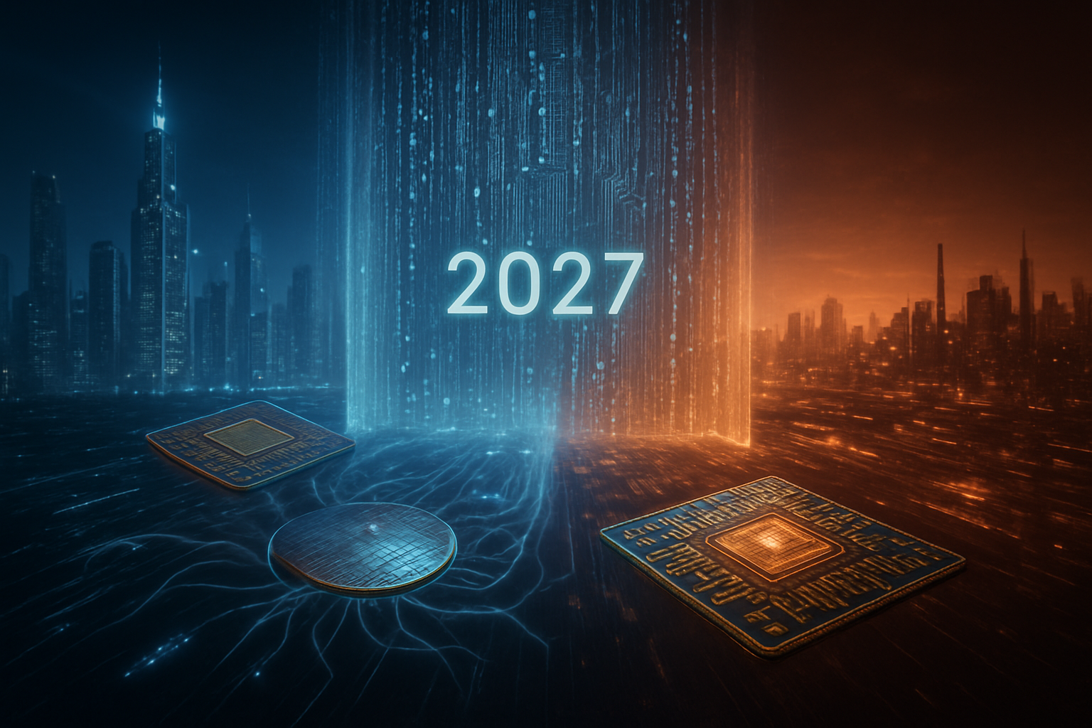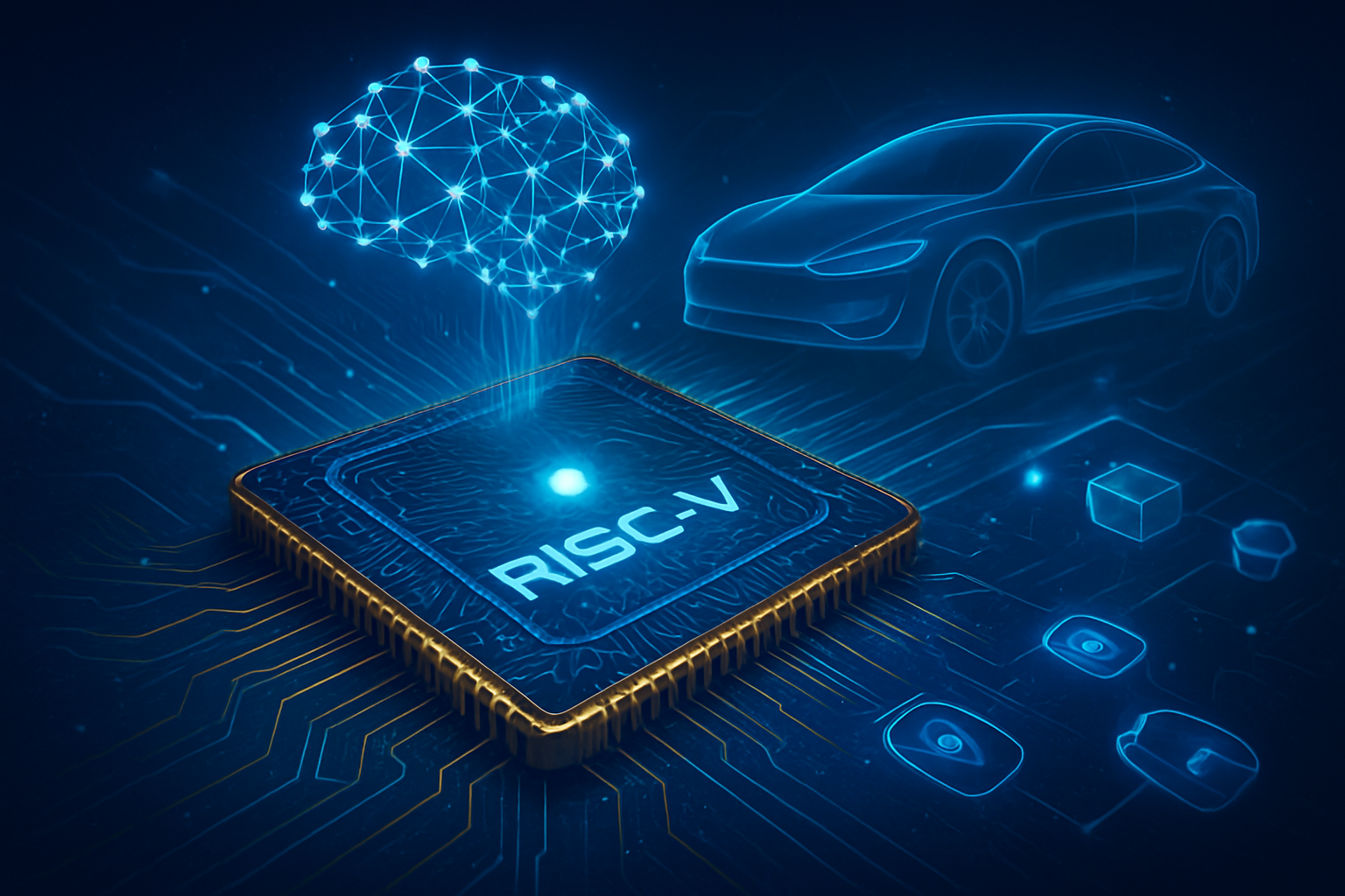
As of late December 2025, the global semiconductor landscape has reached a historic inflection point. Reports emerging from Shenzhen and Beijing confirm that China’s state-led "Manhattan Project" for semiconductor independence has achieved its most critical milestone to date: the successful validation of a domestic Extreme Ultraviolet (EUV) lithography prototype. This breakthrough, occurring just as the year draws to a close, signals a dramatic shift in the "Chip War," suggesting that the technological wall erected by Western export controls is beginning to crumble under the weight of unprecedented state investment and engineering mobilization.
The significance of this development cannot be overstated. For years, the Dutch firm ASML (NASDAQ: ASML) held a global monopoly on the EUV machines required to manufacture the world’s most advanced AI chips. By successfully generating a stable 13.5nm EUV beam using domestically developed light sources, China has moved from a defensive posture of "survival" to an offensive "insurgency." Backed by the $47.5 billion "Big Fund" Phase 3, this mobilization is not merely a corporate endeavor but a national mission overseen by the highest levels of the Central Science and Technology Commission, aimed at ensuring that China’s AI ambitions are no longer beholden to foreign supply chains.
The Technical Frontier: SAQP, SSMB, and the Shenzhen Breakthrough
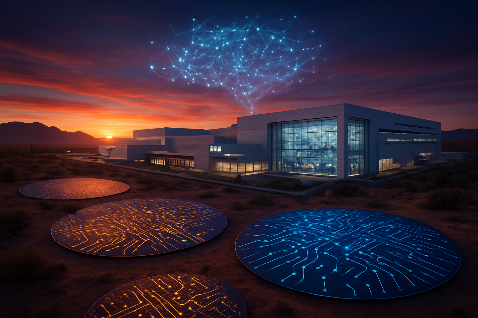
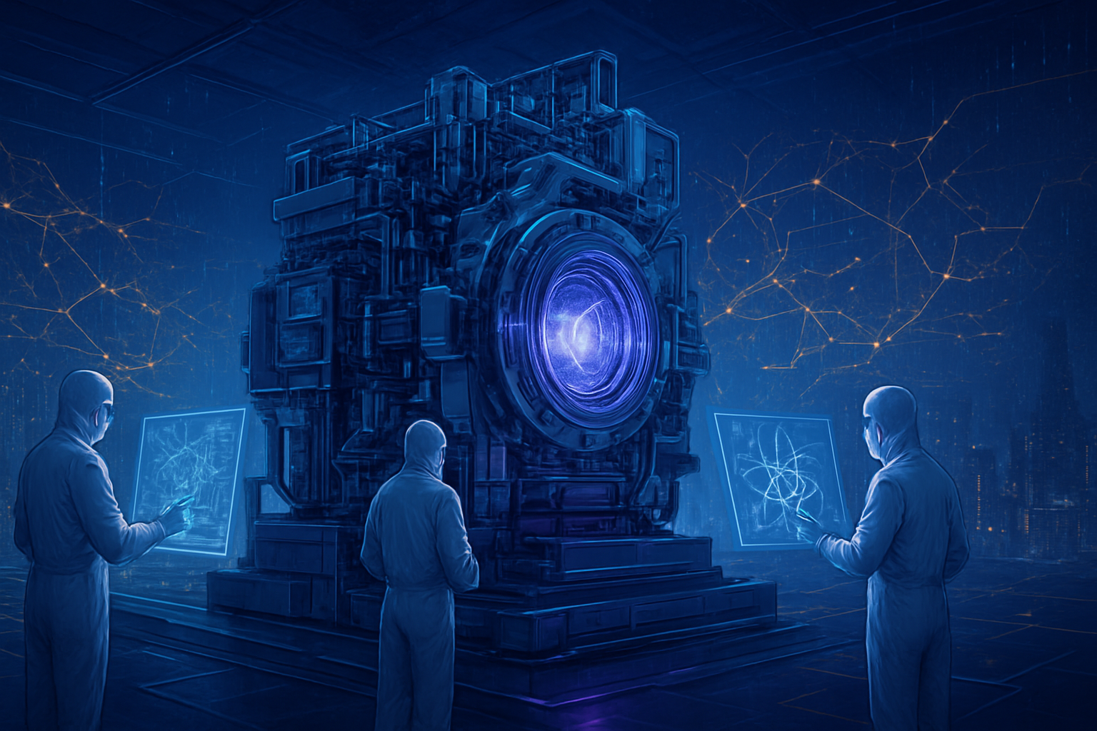
The technical specifications of the new prototype, validated in a high-security facility in Shenzhen, indicate that China is pursuing a dual-track strategy to bypass existing patents. While the current prototype uses a Laser-Induced Discharge Plasma (LDP) system—developed in part by the Harbin Institute of Technology—to vaporize tin and create EUV light, a more ambitious "leapfrog" project is underway in Xiong'an. This secondary project utilizes Steady-State Micro-Bunching (SSMB), a technique that employs a particle accelerator to generate a high-power, continuous EUV beam. Analysts at SemiAnalysis suggest that if successfully scaled, SSMB could theoretically reach power levels exceeding 1kW, potentially surpassing the throughput of current Western lithography standards.
Simultaneously, Chinese foundries led by SMIC (SHA: 601238) have mastered a stopgap technique known as Self-Aligned Quadruple Patterning (SAQP). By using existing Deep Ultraviolet (DUV) machines to print multiple overlapping patterns, SMIC has achieved volume production of 5nm-class chips. While this method is more expensive and has lower yields than native EUV lithography, the massive subsidies from the National Integrated Circuit Industry Investment Fund (the "Big Fund") have effectively neutralized the "technology tax." This has allowed Huawei to launch its latest Mate 80 series and Ascend 950 AI processors using domestic 5nm silicon, proving that high-performance compute is possible even under a total blockade of the most advanced tools.
Initial reactions from the AI research community have been a mix of shock and pragmatic reassessment. Experts who previously predicted China would remain a decade behind the West now acknowledge that the gap has closed to perhaps three to five years. The ability to produce 5nm chips at scale, combined with the successful testing of an EUV light source, suggests that China’s roadmap to 2nm production by 2028 is no longer a propaganda goal, but a credible technical objective. Industry veterans note that the recruitment of thousands of specialized engineers—some reportedly former employees of Western semiconductor firms working under aliases—has been the "secret sauce" in solving the complex precision optics and metrology bottlenecks that define EUV technology.
Market Disruptions: A Bifurcated Global Ecosystem
This development has sent ripples through the boardrooms of Silicon Valley and Hsinchu. For NVIDIA (NASDAQ: NVDA), the emergence of a viable domestic Chinese AI stack represents a direct threat to its long-term dominance. Huawei’s Ascend 910C and 950 series are now being mandated for use in over 50% of Chinese state-owned data centers, leading analysts at Morgan Stanley (NYSE: MS) to project that NVIDIA’s China revenue will remain flat or decline even as global demand for AI continues to surge. The "sovereign AI" movement in China is no longer a theoretical risk; it is a market reality that is carving out a massive, self-contained ecosystem.
Meanwhile, TSMC (NYSE: TSM) is accelerating its pivot toward the United States and Europe to de-risk its exposure to the escalating cross-strait tensions and China’s rising domestic capabilities. While TSMC still maintains a two-node lead with its 2nm production, the loss of market share in the high-volume AI inference segment to SMIC is becoming visible in quarterly earnings. For ASML, the "demand cliff" in China—previously its most profitable region—is forcing a strategic re-evaluation. As Chinese firms like SMEE (Shanghai Micro Electronics Equipment) and Naura Technology Group (SHE: 002371) begin to replace Dutch components in the lithography supply chain, the era of Western equipment manufacturers having unfettered access to the world’s largest chip market appears to be ending.
Startups in the Chinese AI space are the immediate beneficiaries of this "Manhattan Project." Companies specializing in "More-than-Moore" technologies—such as advanced chiplet packaging and 3D stacking—are receiving unprecedented support. By connecting multiple 7nm or 5nm dies using high-bandwidth interconnects like Huawei’s proprietary UnifiedBus, these startups are producing AI accelerators that rival the performance of Western "monolithic" chips. This shift toward advanced packaging allows China to offset its lag in raw lithography resolution by excelling in system-level integration and compute density.
Geopolitics and the New AI Landscape
The wider significance of China’s 2025 breakthroughs lies in the total bifurcation of the global technology landscape. We are witnessing the birth of two entirely separate, incompatible semiconductor ecosystems: one led by the U.S. and its allies (the "Chip 4" alliance), and a vertically integrated, state-driven Chinese stack. This division mirrors the Cold War era but with much higher stakes, as the winner of the "EUV race" will likely dictate the pace of artificial general intelligence (AGI) development. Analysts at Goldman Sachs (NYSE: GS) suggest that China’s progress has effectively neutralized the "total containment" strategy envisioned by 2022-era sanctions.
However, this progress comes with significant concerns. The environmental and energy costs of China’s SSMB particle accelerator projects are enormous, and the intense pressure on domestic engineers has led to reports of extreme "996" work cultures within the state-backed labs. Furthermore, the lack of transparency in China’s "shadow supply chain" makes it difficult for international regulators to track the proliferation of dual-use AI technologies. There is also the risk of a global supply glut in legacy and mid-range nodes (28nm to 7nm), as China ramps up capacity to dominate the foundational layers of the global electronics industry while it perfects its leading-edge EUV tools.
Comparatively, this milestone is being viewed as the semiconductor equivalent of the 1957 Sputnik launch. Just as Sputnik forced the West to revolutionize its aerospace and education sectors, China’s EUV prototype is forcing a massive re-industrialization in the U.S. and Europe. The "Chip War" has evolved from a series of trade restrictions into a full-scale industrial mobilization, where the metric of success is no longer just intellectual property, but the physical ability to manufacture at the atomic scale.
Looking Ahead: The Road to 2nm and Beyond
In the near term, the industry expects China to focus on refining the yield of its 5nm SAQP process while simultaneously preparing its first-generation EUV machines for pilot production in 2026. The Xiong'an SSMB facility is slated for completion by mid-2026, which could provide a centralized "EUV factory" capable of feeding multiple lithography stations at once. If this centralized light-source model works, it could fundamentally change the economics of chip manufacturing, making EUV production more scalable than the current standalone machine model favored by ASML.
Long-term challenges remain, particularly in the realm of precision optics. While China has made strides in generating EUV light, the mirrors required to reflect that light with atomic precision—currently a specialty of Germany’s Zeiss—remain a significant bottleneck. Experts predict that the next two years will be a "war of attrition" in material science, as Chinese researchers attempt to replicate or surpass the multilayer coatings required for high-NA (Numerical Aperture) EUV systems. The goal is clear: by 2030, Beijing intends to be the world leader in both AI software and the silicon that powers it.
Summary and Final Thoughts
The events of late 2025 mark the end of the "sanctions era" and the beginning of the "parallel era." China’s successful validation of an EUV prototype and the mass production of 5nm chips via DUV-based patterning prove that state-led mobilization can overcome even the most stringent export controls. While the West still holds the lead in the absolute frontier of 2nm and High-NA EUV, the gap is no longer an unbridgeable chasm. The "Manhattan Project" for chips has succeeded in its primary goal: ensuring that China cannot be cut off from the future of AI.
As we move into 2026, the tech industry should watch for the first "all-domestic" AI server clusters powered by these new chips. The success of the Xiong'an SSMB facility will be the next major bellwether for China’s ability to leapfrog Western technology. For investors and policymakers alike, the takeaway is clear: the global semiconductor monopoly is over, and the race for silicon sovereignty has only just begun. The coming months will likely see further consolidation of the Chinese supply chain and perhaps a new wave of Western policy responses as the reality of a self-sufficient Chinese AI industry sets in.
This content is intended for informational purposes only and represents analysis of current AI developments.
TokenRing AI delivers enterprise-grade solutions for multi-agent AI workflow orchestration, AI-powered development tools, and seamless remote collaboration platforms.
For more information, visit https://www.tokenring.ai/.