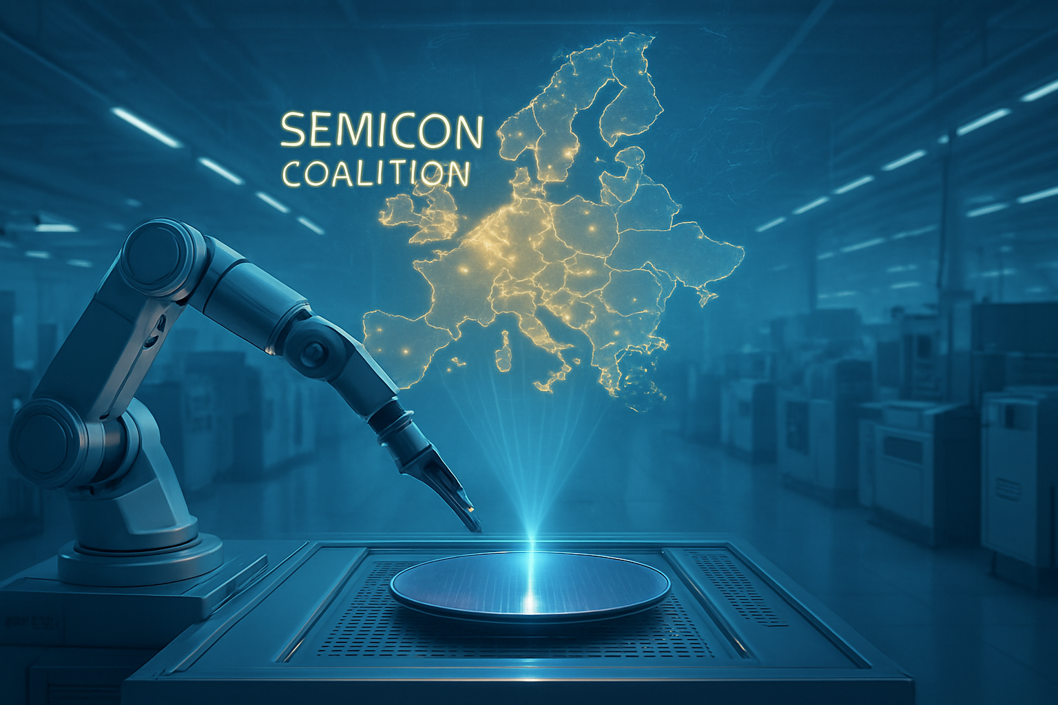
As 2025 draws to a close, the European Union is signaling a massive strategic pivot in its quest for technological autonomy. Building on the foundation of the 2023 European Chips Act, the European Commission has officially laid the groundwork for "EU Chips Act 2.0." This "mid-course correction," as many Brussels insiders call it, aims to bridge the notorious "lab-to-fab" gap—the chasm between Europe's world-leading semiconductor research and its actual industrial manufacturing output. With a formal legislative proposal slated for the first quarter of 2026, the initiative represents a shift from a defensive posture to an assertive industrial policy designed to secure Europe’s place in the global AI hierarchy.
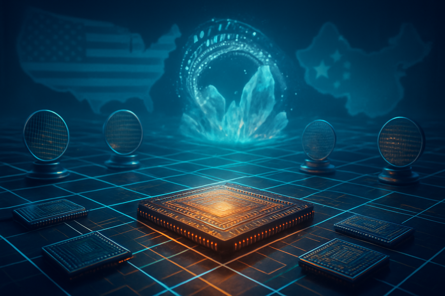
The urgency behind Chips Act 2.0 is driven by a realization that while the original act catalyzed over €80 billion in private and public investment, the target of capturing 20% of the global semiconductor market by 2030 remains elusive. As of December 2024, the global race for AI supremacy has made advanced silicon more than just a commodity; it is now the bedrock of national security and economic resilience. By focusing on streamlined approvals and high-volume fabrication of advanced AI chips, the EU hopes to ensure that the next generation of generative AI models is not just designed in Europe, but powered by chips manufactured on European soil.
Bridging the Chasm: The Technical Pillars of 2.0
The centerpiece of the EU Chips Act 2.0 is the RESOLVE Initiative, a "lab-to-fab" accelerator launched in early 2025 that is now being formalized into law. Unlike previous efforts that focused broadly on capacity, RESOLVE targets 15 specific technology tracks, including 3D heterogeneous integration, advanced memory architectures, and sub-5nm logic. The goal is to create a seamless pipeline where innovations from world-renowned research centers like imec in Belgium, CEA-Leti in France, and Fraunhofer in Germany can be rapidly transitioned to industrial pilot lines and eventually high-volume manufacturing. This addresses a long-standing critique from the European Court of Auditors: that Europe too often "exports its brilliance" to be manufactured by competitors in Asia or the United States.
A critical technical shift in the 2.0 framework is the emphasis on Advanced Packaging. Following recommendations from the updated 2025 "Draghi Report," the EU is prioritizing back-end manufacturing capabilities. As Moore’s Law slows down, the ability to stack chips (3D packaging) has become the primary driver of AI performance. The new legislation proposes a harmonized EU-wide permitting regime to bypass the fragmented national bureaucracies that have historically delayed fab construction. By treating semiconductor facilities as "projects of overriding public interest," the EU aims to move from project notification to groundbreaking in months rather than years, a pace necessary to compete with the rapid expansion seen in the U.S. and China.
Initial reactions from the industry have been cautiously optimistic. Christophe Fouquet, CEO of ASML (NASDAQ: ASML), recently warned that without the faster execution promised by Chips Act 2.0, the EU risks losing its relevance in the global AI race. Similarly, industry lobbies like SEMI Europe have praised the focus on "Fast-Track IPCEIs" (Important Projects of Common European Interest), though they continue to warn against any additional administrative burdens or "sovereignty certifications" that could complicate global supply chains.
The Corporate Landscape: Winners and Strategic Shifts
The move toward Chips Act 2.0 creates a new set of winners in the European tech ecosystem. Traditional European powerhouses like Infineon Technologies (OTCMKTS: IFNNY), NXP Semiconductors (NASDAQ: NXPI), and STMicroelectronics (NYSE: STM) stand to benefit from increased subsidies for "Edge AI" and automotive silicon. However, the 2.0 framework also courts global giants like Intel (NASDAQ: INTC) and TSMC (NYSE: TSM). The EU's push for sub-5nm manufacturing is specifically designed to ensure that these firms continue their expansion in hubs like Magdeburg, Germany, and Dresden, providing the high-end logic chips required for training large-scale AI models.
For major AI labs and startups, the implications are profound. Currently, European AI firms are heavily dependent on Nvidia (NASDAQ: NVDA) and U.S.-based cloud providers for compute resources. The "AI Continent Action Plan," a key component of the 2.0 strategy, aims to foster a domestic alternative. By subsidizing the design and manufacture of European-made high-performance computing (HPC) chips, the EU hopes to create a "sovereign compute" stack. This could potentially disrupt the market positioning of U.S. tech giants by offering European startups a localized, regulation-compliant infrastructure that avoids the complexities of transatlantic data transfers and export controls.
Sovereignty in an Age of Geopolitical Friction
The wider significance of Chips Act 2.0 cannot be overstated. It is a direct response to the weaponization of technology in global trade. Throughout 2025, heightened U.S. export restrictions and China’s facility-level export bans have highlighted the vulnerability of the European supply chain. The EU’s Tech Chief, Henna Virkkunen, has stated that the "top aim" is "indispensability"—creating a scenario where the world relies on European components (like ASML’s lithography machines) as much as Europe relies on external chips.
This strategy mirrors previous AI milestones, such as the launch of the EuroHPC Joint Undertaking, but on a much larger industrial scale. However, concerns remain regarding the "funding gap." While the policy framework is robust, critics argue that the EU lacks the massive capital depth of the U.S. CHIPS and Science Act. The European Court of Auditors issued a sobering report in December 2025, suggesting that the 20% market share target is "very unlikely" without a significant increase in the central EU budget, beyond what member states can provide individually.
The Horizon: What’s Next for European Silicon?
In the near term, the industry is looking toward the official legislative rollout in Q1 2026. This will be the moment when the "lab-to-fab" vision meets the reality of budget negotiations. We can expect to see the first "Fast-Track" permits issued for advanced packaging facilities in late 2026, which will serve as a litmus test for the new harmonized permitting regime. On the applications front, the focus will likely shift toward "Green AI"—chips designed specifically for energy-efficient inference, leveraging Europe’s leadership in power semiconductors to carve out a niche in the global market.
Challenges remain, particularly in workforce development. To run the advanced fabs envisioned in Chips Act 2.0, Europe needs tens of thousands of specialized engineers. Experts predict that the next phase of the policy will involve aggressive "talent visas" and massive investments in university-led semiconductor programs to ensure the "lab" side of the equation remains populated with the world’s best minds.
A New Chapter for the Digital Decade
The transition to EU Chips Act 2.0 marks a pivotal moment in European industrial history. It represents a move away from the fragmented, nation-state approach of the past toward a unified, pan-European strategy for the AI era. By focusing on the "lab-to-fab" pipeline and speeding up the bureaucratic machinery, the EU is attempting to prove that a democratic bloc can move with the speed and scale required by the modern technology landscape.
As we move into 2026, the success of this initiative will be measured not just in euros spent, but in the number of high-end AI chips that roll off European assembly lines. The goal is clear: to ensure that when the history of the AI revolution is written, Europe is a primary author, not just a reader.
This content is intended for informational purposes only and represents analysis of current AI developments.
TokenRing AI delivers enterprise-grade solutions for multi-agent AI workflow orchestration, AI-powered development tools, and seamless remote collaboration platforms.
For more information, visit https://www.tokenring.ai/.