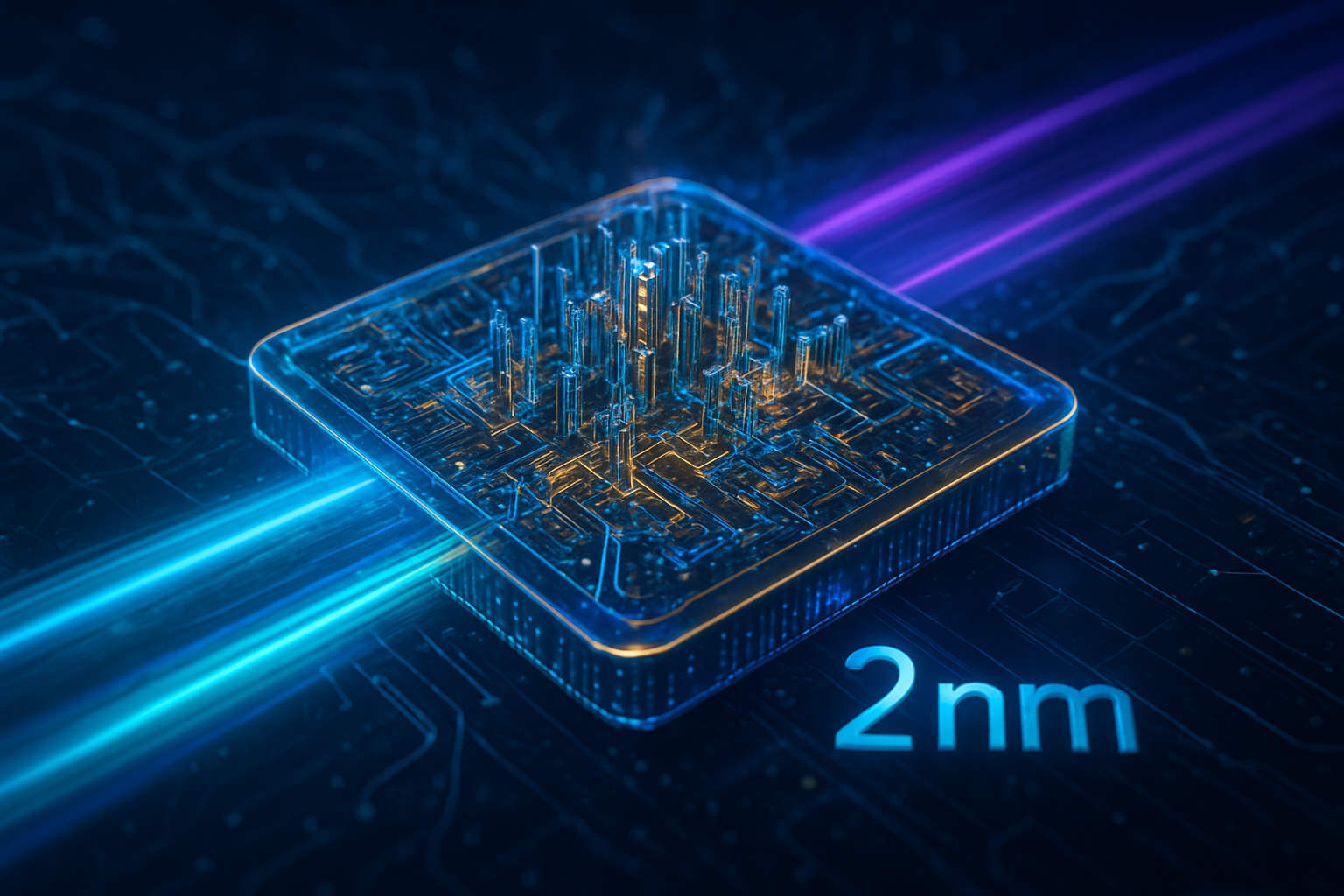
As of December 24, 2025, the semiconductor industry has reached a fever pitch in what analysts are calling the most consequential transition in the history of silicon manufacturing. The race to dominate the 2-nanometer (2nm) era is no longer a theoretical roadmap; it is a high-stakes reality. Taiwan Semiconductor Manufacturing Company (TSMC) (NYSE: TSM) has officially entered high-volume manufacturing (HVM) for its N2 process, while Samsung Electronics (KRX: 005930) is aggressively positioning its second-generation 2nm node (SF2P) to capture the exploding demand for artificial intelligence (AI) infrastructure and flagship mobile devices.
This shift represents more than just a minor size reduction. It marks the industry's collective move toward Gate-All-Around (GAA) transistor architecture, a fundamental redesign of the transistor itself to overcome the physical limitations of the aging FinFET design. With AI server racks now demanding unprecedented power levels and flagship smartphones requiring more efficient on-device neural processing, the winner of this 2nm sprint will essentially dictate the pace of AI evolution for the remainder of the decade.
The move to 2nm is defined by the transition from FinFET to GAAFET (Gate-All-Around Field-Effect Transistor) or "nanosheet" architecture. TSMC’s N2 process, which reached mass production in the fourth quarter of 2025, marks the company's first jump into nanosheets. By wrapping the gate around all four sides of the channel, TSMC has achieved a 10–15% speed improvement and a 25–30% reduction in power consumption compared to its 3nm (N3E) node. Initial yield reports for TSMC's N2 are remarkably strong, with internal data suggesting yields as high as 80% for early commercial batches, a feat attributed to the company's cautious, iterative approach to the new architecture.
Samsung, conversely, is leveraging what it calls a "generational head start." Having introduced GAA technology at the 3nm stage, Samsung’s SF2 and its enhanced SF2P processes are technically third-generation GAA designs. This experience has allowed Samsung to offer Multi-Bridge Channel FET (MBCFET), which provides designers with greater flexibility to vary nanosheet widths to optimize for either extreme performance or ultra-low power. While Samsung’s yields have historically lagged behind TSMC’s, the company reported a breakthrough in late 2025, reaching a stable 60% yield for its SF2 node, which is currently powering the Exynos 2600 for the upcoming Galaxy S26 series.
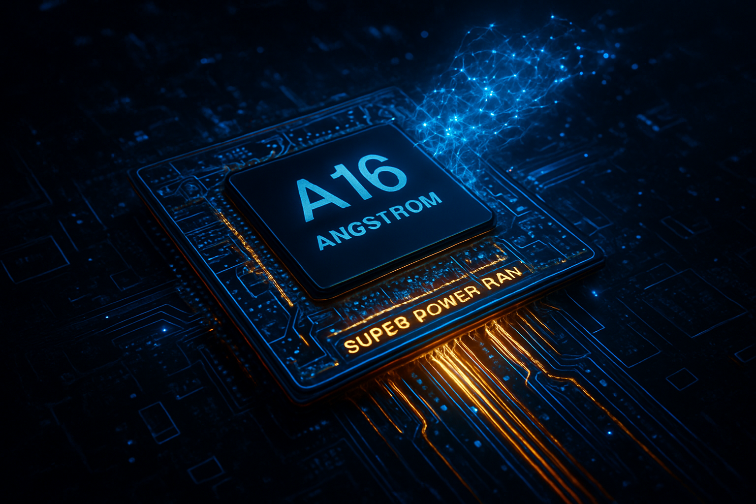
Industry experts have noted that the 2nm era also introduces "Backside Power Delivery" (BSPDN) as a critical secondary innovation. While TSMC has reserved its "Super Power Rail" for its enhanced N2P and A16 (1.6nm) nodes expected in late 2026, Intel (NASDAQ: INTC) has already pioneered this with its "PowerVia" technology on the 18A node. This separation of power and signal lines is essential for AI chips, as it drastically reduces "voltage droop," allowing chips to maintain higher clock speeds under the massive workloads required for Large Language Model (LLM) training.
Initial reactions from the AI research community have been overwhelmingly focused on the thermal implications. At the 2nm level, power density has become so extreme that air cooling is increasingly viewed as obsolete for data center applications. The consensus among hardware architects is that 2nm AI accelerators, such as NVIDIA's (NASDAQ: NVDA) projected "Rubin" series, will necessitate a mandatory shift to direct-to-chip liquid cooling to prevent thermal throttling during intensive training cycles.
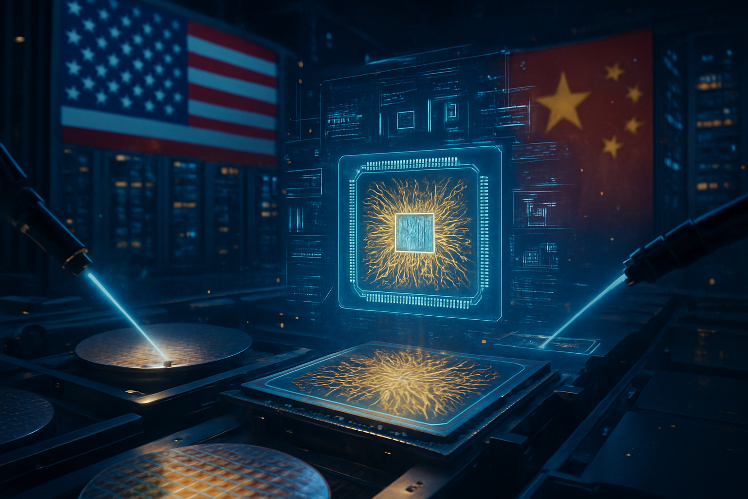
The competitive landscape for 2nm is characterized by a fierce tug-of-war over the world's most valuable tech giants. TSMC remains the dominant force, with Apple (NASDAQ: AAPL) serving as its "alpha customer." Apple has reportedly secured nearly 50% of TSMC’s initial 2nm capacity for its A20 and A20 Pro chips, which will debut in the iPhone 18. This partnership ensures that Apple maintains its lead in on-device AI performance, providing the hardware foundation for more complex, autonomous Siri agents.
However, Samsung is making strategic inroads by targeting the "Big Tech" hyperscalers. Samsung is currently running Multi-Project Wafer (MPW) sample tests with AMD (NASDAQ: AMD) for its second-generation SF2P node. AMD is reportedly pursuing a "dual-foundry" strategy, using TSMC for its Zen 6 "Venice" server CPUs while exploring Samsung’s 2nm for its next-generation Ryzen processors to mitigate supply chain risks. Similarly, Google (NASDAQ: GOOGL) is in deep negotiations with Samsung to produce its custom AI Tensor Processing Units (TPUs) at Samsung’s nearly completed facility in Taylor, Texas.
Samsung’s Taylor fab has become a significant strategic advantage. Under Taiwan’s "N-2" policy, TSMC is required to keep its most advanced manufacturing technology in Taiwan for at least two years before exporting it to overseas facilities. This means TSMC’s Arizona plant will not produce 2nm chips until at least 2027. Samsung, however, is positioning its Texas fab as the only facility in the United States capable of mass-producing 2nm silicon in 2026. For US-based companies like Google and Meta (NASDAQ: META) that are under pressure to secure domestic supply chains, Samsung’s US-based 2nm capacity is an attractive alternative to TSMC’s Taiwan-centric production.
Market dynamics are also being shaped by pricing. TSMC’s 2nm wafers are estimated to cost upwards of $30,000 each, a 50% increase over 3nm prices. Samsung has responded with an aggressive pricing model, reportedly undercutting TSMC by roughly 33%, with SF2 wafers priced near $20,000. This pricing gap is forcing many AI startups and second-tier chip designers to reconsider their loyalty to TSMC, potentially leading to a more fragmented and competitive foundry market.
The significance of the 2nm transition extends far beyond corporate rivalry; it is a vital necessity for the survival of the AI boom. As LLMs scale toward tens of trillions of parameters, the energy requirements for training and inference have reached a breaking point. Gartner predicts that by 2027, nearly 40% of existing AI data centers will be operationally constrained by power availability. The 2nm node is the industry's primary weapon against this "power wall."
By delivering a 30% reduction in power consumption, 2nm chips allow data center operators to pack more compute density into existing power envelopes. This is particularly critical for the transition from "Generative AI" to "Agentic AI"—autonomous systems that can reason and execute tasks in real-time. These agents require constant, low-latency background processing that would be prohibitively expensive and energy-intensive on 3nm or 5nm hardware. The efficiency of 2nm silicon is the "gating factor" that will determine whether AI agents become ubiquitous or remain limited to high-end enterprise applications.
Furthermore, the 2nm era is coinciding with the integration of HBM4 (High Bandwidth Memory). The combination of 2nm logic and HBM4 is expected to provide over 15 TB/s of bandwidth, allowing massive models to fit into smaller GPU clusters. This reduces the communication latency that currently plagues large-scale AI training. Compared to the 7nm milestone that enabled the first wave of deep learning, or the 5nm node that powered the ChatGPT explosion, the 2nm breakthrough is being viewed as the "efficiency milestone" that makes AI economically sustainable at a global scale.
However, the move to 2nm also raises concerns regarding the "Economic Wall." As wafer costs soar, the barrier to entry for custom silicon is rising. Only the wealthiest corporations can afford to design and manufacture at 2nm, potentially leading to a concentration of AI power among a handful of "Silicon Superpowers." This has prompted a surge in chiplet-based designs, where only the most critical compute dies are built on 2nm, while less sensitive components remain on older, cheaper nodes.
Looking ahead, the 2nm sprint is merely a precursor to the 1.4nm (A14) era. Both TSMC and Samsung have already begun outlining their 1.4nm roadmaps, with production targets set for 2027 and 2028. These future nodes will rely heavily on High-NA (Numerical Aperture) Extreme Ultraviolet (EUV) lithography, a next-generation manufacturing technology that allows for even finer circuit patterns. Intel has already taken delivery of the world’s first High-NA EUV machines, signaling that the three-way battle for silicon supremacy will only intensify.
In the near term, the industry is watching for the first 2nm-powered AI accelerators to hit the market in mid-2026. These chips are expected to enable "World Models"—AI systems that can simulate physical reality with high fidelity, a prerequisite for advanced robotics and autonomous vehicles. The challenge remains the complexity of the manufacturing process; as transistors approach the size of a few dozen atoms, quantum tunneling and other physical anomalies become increasingly difficult to manage.
Predicting the next phase, analysts suggest that the focus will shift from raw transistor density to "System-on-Wafer" technologies. Rather than individual chips, foundries may begin producing entire wafers as single, interconnected AI processing units. This would eliminate the bottlenecks of traditional chip packaging, but it requires the near-perfect yields that TSMC and Samsung are currently fighting to achieve at the 2nm level.
The 2nm sprint represents a pivotal moment in the history of computing. TSMC’s successful entry into high-volume manufacturing with its N2 node secures its position as the industry’s reliable powerhouse, while Samsung’s aggressive testing of its second-generation GAA process and its strategic US-based production in Texas offer a compelling alternative for a geopolitically sensitive world. The key takeaways from this race are clear: the architecture of the transistor has changed forever, and the energy efficiency of 2nm silicon is now the primary currency of the AI era.
In the context of AI history, the 2nm breakthrough will likely be remembered as the point where hardware finally began to catch up with the soaring ambitions of software architects. It provides the thermal and electrical headroom necessary for the next generation of autonomous agents and trillion-parameter models to move from research labs into the pockets and desktops of billions of users.
In the coming weeks and months, the industry will be watching for the first production samples from Samsung’s Taylor fab and the final performance benchmarks of Apple’s A20 silicon. As the first 2nm chips begin to roll off the assembly lines, the race for next-gen silicon will move from the cleanrooms of Hsinchu and Pyeongtaek to the data centers and smartphones that define modern life. The sprint is over; the 2nm era has begun.
This content is intended for informational purposes only and represents analysis of current AI developments.
TokenRing AI delivers enterprise-grade solutions for multi-agent AI workflow orchestration, AI-powered development tools, and seamless remote collaboration platforms.
For more information, visit https://www.tokenring.ai/.